HAL Id: hal-01646807
https://hal.archives-ouvertes.fr/hal-01646807
Submitted on 23 Nov 2017HAL is a multi-disciplinary open access archive for the deposit and dissemination of sci-entific research documents, whether they are pub-lished or not. The documents may come from teaching and research institutions in France or abroad, or from public or private research centers.
L’archive ouverte pluridisciplinaire HAL, est destinée au dépôt et à la diffusion de documents scientifiques de niveau recherche, publiés ou non, émanant des établissements d’enseignement et de recherche français ou étrangers, des laboratoires publics ou privés.
Design of a SiC based triple active bridge ceil for a
multi-megawatt DC-DC converter
Jose Maneiro, Roland Ryndzionek, Thomas Lagier, Piotr Dworakowski, Cyril
Buttay
To cite this version:
Jose Maneiro, Roland Ryndzionek, Thomas Lagier, Piotr Dworakowski, Cyril Buttay. Design of a SiC based triple active bridge ceil for a multi-megawatt DC-DC converter. EPE’17 ECCE Europe, Sep 2017, Warsaw, Poland. �10.23919/EPE17ECCEEurope.2017.8099005�. �hal-01646807�
Design of a SiC based Triple Active Bridge cell for a multi-megawatt
DC-DC converter
Jose Maneiro
§, Roland Ryndzionek
*, §, Thomas Lagier
§, Piotr Dworakowski
§,
Cyril Buttay
†, § §SuperGrid Institute
21 Rue Cyprian, 69100
Villeurbanne, France
jose.maneiro@supergrid-institute.com
www.supergrid-institute.com
*Gdansk University of
Technology
11/12 Gabriela Narutowicza,
80-233
Gdansk, Poland
†Université de Lyon
CNRS, INSA-Lyon,
Laboratoire AMPÈRE
UMR 5005, F-69621
Villeurbanne, France
Acknowledgements
This work was supported by a grant overseen by the French National Research Agency (ANR) as part of the “Investissements d’Avenir” Program (ANE-ITE-002-01). The authors would equally like to thank DEEP Concept, Seccom and Aavid Thermalloy for they support with the design of the converter prototype.
Keywords
« High voltage power converters », « DC collector network », « HVDC », « Renewable energy systems ».
Abstract
The paper describes the design methodology of a novel Triple Active Bridge cell used as the building block for modular DC-DC converters. The intended application is for Medium Voltage Direct Current grids, such as the DC collector for offshore wind farms. The latest generation of SiC MOSFET semiconductors is utilized to operate in the medium frequency range while optimizing the efficiency. The dimensioning of the main cell components, including semiconductors, transformer and DC capacitors is presented. The cell mechanical integration and cooling are also addressed.
Introduction
A new battle in the War of Currents [1], with Edison's direct current (DC) and Westinghouse's alternating current (AC) at the origin, has begun. The arrival of new power semiconductors, such as thyristors and IGBTs, and the development of electronics and computer science, have been the main triggers. The transmission of bulk power over very long distances is now reserved to high voltage direct current (HVDC) [2] with voltages reaching 800 kV. Meanwhile, the USB standard with its 5V DC is expanding in domestic applications. Thanks to the technological improvements in wide bandgap semiconductors, such as the Silicon Carbide (SiC) [3], an increasing number of applications may switch to DC in the coming years. Numerous research projects and some industrial projects target DC-DC power converters as a key component of the electrical networks. The DC-DC converters are often proposed for green energy and transportation applications such as photovoltaic [4], electric vehicles [5], wind power [6] and railway electric traction [7]. The offshore wind DC collector appears to be a cost effective solution as it allows to reduce the volume and weight on the offshore platforms [8] and could be one of the first multi-terminal DC (MTDC) grids to be introduced.
The Dual Active Bridge (DAB) converter [9] is one of the most promising DC-DC circuit topologies for high power applications. The series and/or parallel connection of elementary DABs allows to increase the voltage and power to build converters well suited for medium voltage DC (MVDC) and potentially extensible to high voltage DC (HVDC) applications [10], [11]. The main challenge of this multi-cell topology is the medium frequency transformer (MFT) insulation, especially for HVDC
applications. Even if a high voltage
insulated
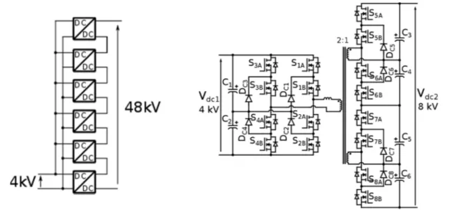
MFT has been reported [12] it seems that for the moment these multi cell converters are more viable for MVDC applications.This article focuses on the medium voltage DC-DC converter for an “all DC” offshore windfarm conversion chain (Fig. 1). Assuming similar insulation constraints as for a 66 kV AC collector [13], an offshore DC collection grid of ±48 kV is envisaged. On the other hand a possible evolution of wind generators to 10 MW power and 4 kV DC output is used as the reference to finalize the converter specification. The design methodology of such DC-DC converter to step up the wind generator output voltage to MVDC levels is presented in the following sections. These results are being used for the design of a full scale demonstration prototype.
a. Offshore AC collector concept. b. Offshore DC collector concept. Fig. 1 – Offshore windfarm conversion chain evolution towards an all DC solution.
The Neutral Point Clamped Triple Active Bridge Cell
The cascaded multi-cell topology from Fig. 2a, an input-parallel output-series (IPOS) configuration, is selected to implement a 4 kV to 48 kV DC-DC step-up converter. Whilst keeping the good performance of the conventional DAB cell, the triple active bridge (TAB) [14], displayed in Fig. 2b, helps achieving the required transformation ratio of 12 with the minimum number of cells and overall number of components.
a. Cascaded IPOS structure of one pole of the full converter.
b. TAB cell, based on 3.3kV transistors and diodes connected in NPC configuration.
Fig. 2 – Multi-cell structure and TAB cell detail.
Considering the six cells in IPOS configuration used to build a 4.8 MW converter, the resulting cell nominal ratings are displayed in Table I. A medium frequency operation at 20 kHz is selected for the AC link to reduce the size of both inductive and capacitive elements [15]. A ±10% variation in either DC bus voltages is also permitted during normal operation.
Table I – TAB cell nominal ratings.
Low voltage DC port 4 kV ±10%
Medium voltage DC port 8 kV ±10%
Rated power 800 kW
AC frequency 20 kHz
Cell modulation strategy
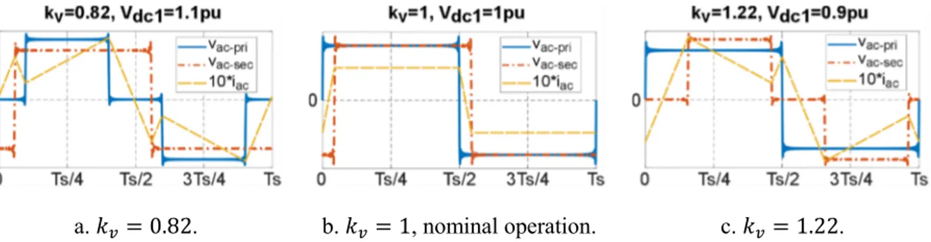
A simple modulation approach is proposed to minimize the RMS current value in the AC link. By adjusting the square voltage pulse width, defined by angle in Fig. 3, the amplitude of the 20 kHz fundamental components of the voltage in both primary and secondary windings is made equal. Two regions of operation are then identified based on the primary/secondary voltage ratio defined in (1), where 0.5 is the transformation ratio of the MFT windings. These are represented in Fig. 3a for the case 1, and Fig. 3b for 1. Expressions (2) and (3) define the primary and secondary voltage pulse widths inside each operation region respectively. The active power flow is controlled with the phase shift also represented in Fig. 3. The nominal point of operation is defined for 1. As presented in (4), in this case the widths of both voltage pulses and are equal with a value of , or 25 s for operation at 20kHz.
a. Operation with 1. b. Operation with 1.
Fig. 3 – Detail of proposed TAB cell modulation. 0.5 ∙
(1)
If 1: 2 ∙ arcsin , (2)
If 1: , 2 ∙ arcsin (3)
If 1: , (4)
Fig. 4 presents the resulting AC voltages and currents at the nominal point of operation (Fig. 4b) and the two extreme points during degraded mode of operation ( 1) caused by the allowed voltage variation in both DC buses of ±10%.
a. 0.82. b. 1, nominal operation. c. 1.22.
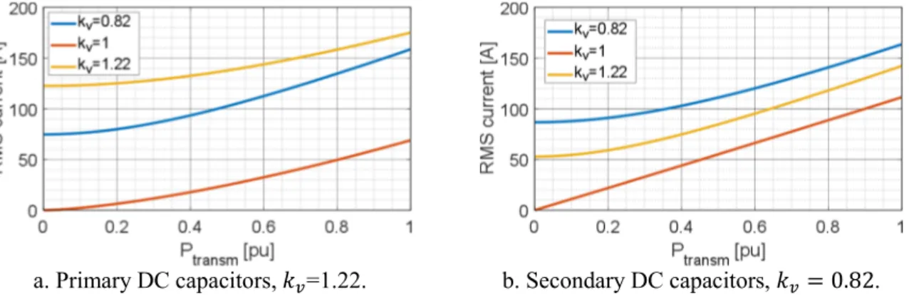
In Fig. 5 the resulting RMS currents in the transformer windings are presented for the proposed modulation strategy ( -mod.) and also for the conventional square modulation (square-mod.) [16]. During nominal operation at 1 both modulations generate identical voltage pulses at the transformer windings and therefore the resulting AC currents are also identical. Contrarily, during degraded operation ( =0.82 and =1.22) the proposed modulation achieves a reduction on the RMS value of the current as observed. The reduction is significant for low power transfers which translates in a reduction of the power losses in semiconductors, transformer and DC capacitors, improving the overall TAB cell efficiency.
Fig. 5 – AC current RMS value as a function of the cell transmitted power for both the proposed modulation and the conventional square modulation.
Medium frequency transformer and DC capacitors
A single phase transformer with two secondary windings is employed in the TAB cell (Fig. 6). The design uses a medium frequency magnetic core material and solid insulation in order to provide the required primary-secondary insulation level. The resulting design parameters are displayed in Table 2. The complete transformer assembly is water cooled.
Table II – Transformer ratings.
Rated power 1 MVA
Rated frequency 20 kHz
Pri. rated voltage ±4 kV
Sec. rated voltage ±2 kV
Insulation pri.-sec. 80 kV
Leakage inductance pri.-sec. 75 H Fig. 6 – MFT structure.
The DC capacitors are dimensioned for a maximum peak-to-peak voltage ripple of 5% under the degraded mode operation. The RMS current evolution is displayed in Fig. 7a for the primary bridge capacitors and in Fig. 7b for the secondary bridges.
a. Primary DC capacitors, =1.22. b. Secondary DC capacitors, 0.82. Fig. 7 – DC filter capacitors RMS current evolution for nominal and degraded modes of operation.
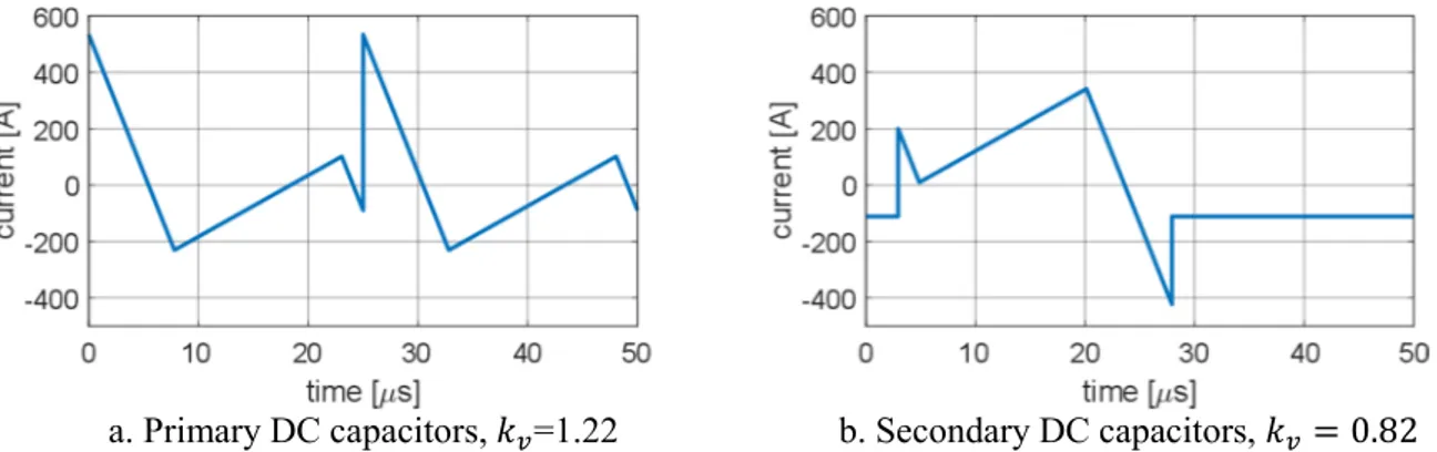
The instantaneous periodic current waveforms through the primary/secondary bridge capacitors are displayed in Fig. 8, where the peak current values needed for the capacitor sizing are observed.
a. Primary DC capacitors, =1.22 b. Secondary DC capacitors, 0.82 Fig. 8 –DC capacitor instantaneous current at nominal power transmission during degraded modes of operation.
Metallised polypropylene film technology offers the best performance for operation at medium frequency with the required voltage and current ratings for this application. Each capacitor C1 to C6 (Fig. 2b) is then implemented using four parallel capacitors with the ratings displayed in Table III.
Table III – DC capacitor ratings.
Capacitance 22.5 F
Max. voltage 3.3 kV
RMS current (@20 kHz) 50 A
Equivalent series resistance (ESR) < 3 mΩ
Equivalent series inductance (ESL) < 50 nH
Sizing of semiconductor switches
To achieve the medium frequency operation with a target efficiency of 99% SiC MOSFET switches are selected. At the time of writing, the latest generation of 3.3 kV MOSFET dies, offering a drain-source on-state resistance of 45 mΩ, present a better cost/performance ratio than their 6.5 kV or 10 kV counterparts. The use of a Neutral Point Clamped (NPC) structure (Fig. 2b) is therefore needed to reach the required blocking voltages in the TAB cell. In addition, the use of full-bridge configuration on the primary and a half-bridge configuration on the secondary of the cell, together with the 2:1 ratio in the transformer windings, results in the same current rating for all semiconductor switches in the cell.
a. Wind turbine average power output
calculation. b. Economical gain comparison for different number of dies per MOSFET switch. Fig. 9 – Results of the cost benefit analysis to optimize the required number of parallel dies per MOSFET switch.
The main source of power losses in the TAB cell are the conduction and switching losses in the MOSFETs. When using SiC devices conduction losses are dominant. By increasing the number of parallel dies that compose a MOSFET switch, the equivalent drain-source ON state resistance ( ) of the resulting switch is reduced. As a result the conduction losses are also reduced, and the TAB cell efficiency increases. A trade-off exists therefore between the number of parallel dies to be used in the converter design and the incurred extra cost.
In this case, the design of the semiconductor switches has been optimized for the offshore DC collector application. The wind speed probability distribution function of a particular location (displayed in red in Fig. 9a) is combined according to expression (5) with the WTG power output characteristic (in blue in Fig. 9a), previously modified with the efficiency curve of the TAB cell (Fig. 11b) for a particular number of parallel dies per switch.
∙ (5)
In this way, the power losses in the DC-DC converter are already factored in the resulting averaged power. The averaged power is then used to calculate the total energy generation by the wind turbine over the period of one year and the result is capitalized according to the current offshore wind feed-in tariffs in France (13 c€/kWh for the 1st 10 years, 3 c€/kWh after). The process is then repeated by increasing the number of parallel dies and the extra income obtained by the increased efficiency of the DC-DC converter is computed. The results of this cost-benefit analysis are displayed in Fig. 9b for designs using between 3 and 10 dies per switch. To assess the economic interest of a particular design, the savings for a particular time frame of up to 30 years are presented. The extra cost of adding 1 additional SiC MOSFET die per switch in all converter switches is also represented (red line). The value considers the forecasted cost reduction ($3.6/Amp) for 3.3kV SiC MOSFET dies in volume production [17]. For the particular case of the TAB cell presented here, a design employing 6 parallel dies per MOSFET switch was chosen, which as observed in Fig. 9b, allows to recover the incurred extra cost considering volume production prices in less than 10 years.
Cell efficiency and cooling
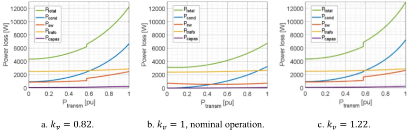
The resulting power losses in the TAB cell using 6 dies per MOSFET switch are then computed and presented in Fig. 10 for the nominal and degraded modes of operation. The figures include the losses in the MFT (yellow) and DC capacitors (purple) as well as the switching (red) and conduction (blue) losses in the cell semiconductors. The steps observed in the curves correspond to the crossing of the soft-switching region for the degraded modes of operation. As observed, the resulting total cell losses (green) at nominal power transfer (800 kW) are in the region of 7 kW for the nominal operation which increase to 13 kW for degraded mode operation at =1.22.
a. 0.82. b. 1, nominal operation. c. 1.22.
Fig. 10 – Detail of cell losses during nominal and degraded modes of operation.
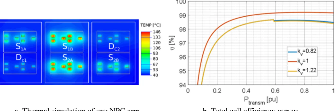
A liquid cooling system is designed to evacuate the losses in the TAB cell, which include the losses in the semiconductor switches and the MFT. Fig. 12a shows the thermal simulation for a liquid cold plate
with the three power modules that implement a complete NPC arm. The cold plate internal channels, pressure drop and coolant flow rate are adjusted to minimize the MOSFET junction temperature under nominal operation while keeping the junction temperature below 175°C under the worst case operation during degraded modes. The final design presents an equivalent thermal resistance junction to coolant fluid of =0.64 K/W. The resulting TAB cell efficiency curves considering transformer and capacitor losses for nominal and degraded modes are displayed in Fig. 11b. This verifies that the target efficiency of 99% for nominal operation is achieved.
a. Thermal simulation of one NPC arm. b. Total cell efficiency curves. Fig. 11 – Power module thermal simulations and total cell efficiency.
The individual junction temperatures of the cell semiconductors are displayed in Fig. 12. The results validate the correct design of the cooling system. In the graphs a distinction is made between the primary and secondary bridge switches (pri/sec), as well as for the inner and outer MOSFET switches in the NPC arm (Sin/Sout), due to the uneven losses distribution among them when employing the proposed modulation. The temperature in the clamping diodes (Dc) is also displayed.
a. 0.82. b. 1, nominal operation. c. 1.22.
Fig. 12 – Detail of cell losses during nominal and degraded modes of operation.
Mechanical Integration of the TAB Cell
The converter described here combines several features which are usually not seen together: high power (800 kW), high switching frequency (20 kHz) and the NPC topology. This requires to split the active devices over several modules due to the high power. At the same time due to the high frequency of operation, the parasitic inductances need to be reduced as much as possible. The design of the power modules and the busbars is therefore studied as a whole in order to find the best compromise that minimizes the transient over-voltages during commutation.
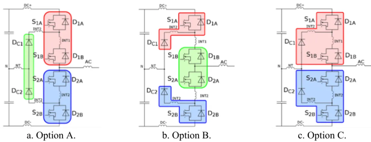
Different cell arm configurations
The semiconductors switched are packed as a half-bridge structure. Fig. 5 presents three possible configurations of power modules studied for the NPC arm.
a. Option A. b. Option B. c. Option C. Fig. 13 –Three possible configurations for grouping the semiconductors in two or three power modules to form a NPC half-bridge.
It is possible to minimize parasitic inductances, shorten the busbar length, obtain better flexibility or reduce the inverter cost by choosing the optimal mechanical arrangement of the arm. In order to find the best compromise, simplified simulations have been performed using Ansys® Simplorer [18]. In these simulations, parasitic inductances have been estimated according to the mechanical layout for each option. For example, when the electrical connection between two switches is achieved internally in the power module, the parasitic inductance between these two switches is lower than it would have been achieved externally, by using a busbar. Fig. 14 presents the simulation results of the resulting voltage overshoot across the switches for the three configurations of Fig. 13 during a switching event.
Peak voltage
S
1AS
1BA 715 V 590 V B 580 V 575 V C 570 V 480 V
Fig. 14 –Voltage overshoot during turn-off of switches S1A and S1B (Vdc1 = 4 kV and Id = 300 A). In terms of parasitic inductances the best choice is option C. However, this is not compatible with existing modules in terms of internal layouts (most high power modules can host one or two sets of semiconductors, not three) and voltage ratings (the module in configuration C experiences the full DC voltage of the half bridge). On the contrary, options A and B can be implemented using standard industrial power modules. For this project the industry standard XHPTM outline introduced by Infineon is used. A good compromise for the TAB cell is found with option B (Fig. 13b). In the NPC arm, the currents flowing through S1A and S2B shift to DC1 and DC2 at turn off. To reduce the parasitic inductances due to the long current loop, S1A/DC1 and S2B/DC2 are packed together. A third power module contains S1B/S2A.
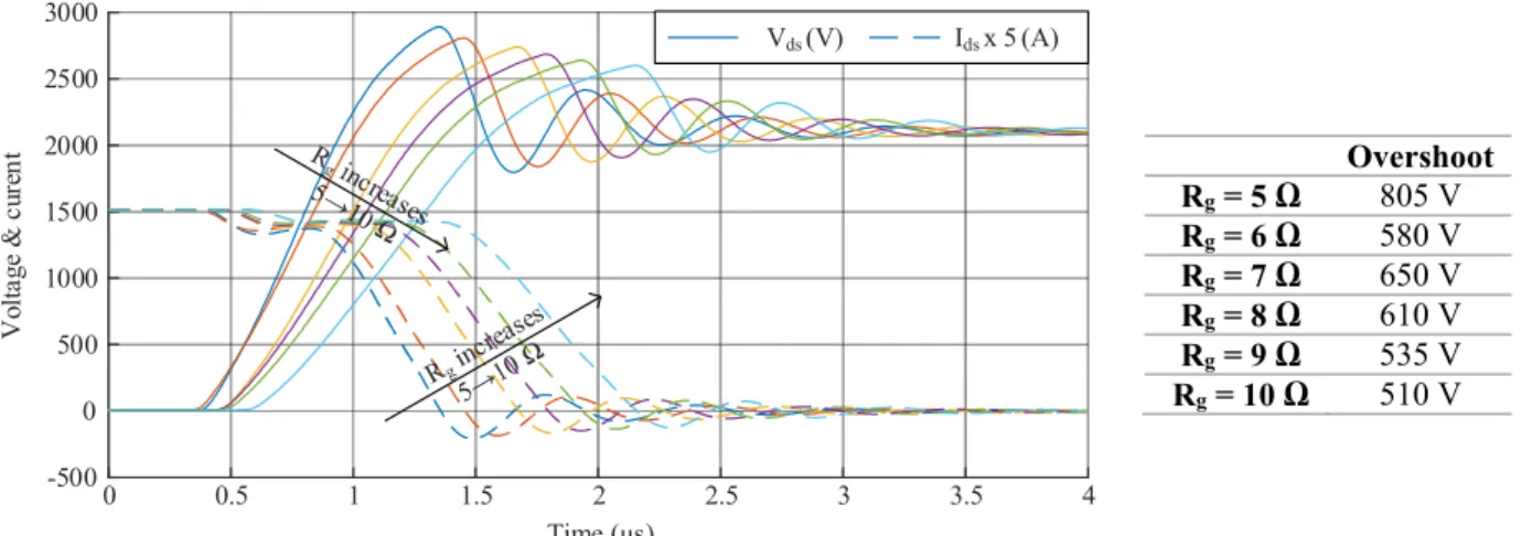
Sensitivity to gate resistance value
Once the system is designed, electro-magnetic simulations have been carried out in order to validate the mechanical design. As presented before, parasitic inductances are a key parameter with high speed switching devices such as SiC MOSFETs. Consequently, the simulation models integrate the reduced RLC models of the busbars and the electrical connections allowing the consideration of the parasitic elements. To obtain the RLC model, finite element simulations were performed with the Ansys® Q3D environment [18]. In the temporal simulation software environment, behavioural models of the SiC MOSFET have been developed thanks to the datasheets and measurements performed on the power modules [19].
Option A Option B Option C
Time (µs) 20 20.1 20.2 20.3 20.4 20.5 Vo lta ge ( kV) 1.5 2 2.5 Time (µs) 24 24.1 24.2 24.3 24.4 24.5 Vo lta ge ( kV) 1.5 2 2.5
S
1AS
1BOvershoot Rg = 5 Ω 805 V Rg = 6 Ω 580 V Rg = 7 Ω 650 V Rg = 8 Ω 610 V Rg = 9 Ω 535 V Rg = 10 Ω 510 V
Fig. 15 – Voltage and current waveforms during the turn-off of S1B, for several values of gate resistance (VDC1 = 4 kV – I = 300 A).
Fig. 15 presents voltage and current waveforms across switch S1B during turn-off for several values of gate resistance (Rg). As observed, the slowing down in the commutation speed when increasing Rg helps reducing the voltage overshoot. A small voltage unbalance is also observed at the end of the commutation (the voltage after the commutation is 2090 V whereas it should be 2000 V). This unbalance is caused by the difference on the commutation loop inductance of switches S1A and S1B. Considering the nominal value of the voltage across the switch, the unbalance is negligible. However, if required, the gate resistance value may be adapted in order to reduce it. The simulation results give a total commutation loop inductance value of 120 nH for the selected pack configuration and busbar design (Fig. 16a). This value takes into account the loop formed by the DC filter capacitors, the busbar and the power modules. The real implementation of the full-bridge primary inverter is displayed in Fig. 16b.
a. 3D model of the primary inverter. b. Primary inverter on the test bench. Fig. 16 – CAD model and real implementation of the primary inverter of the TAB cell.
Conclusions
The paper presents the design methodology of a triple active bridge (TAB) cell. The cell is used as the building block for the implementation of modular DC-DC converters in MVDC applications. The required ratings of the different elements integrating the cell are identified. An optimal design of the semiconductor power modules relies on a cost-benefit analysis of the offshore wind DC collector application. The optimal number of SiC MOSFET dies to be used per switch is found to be six. With the power module design fixed, the power losses in the different cell elements are estimated in order to obtain the total cell efficiency curves. The power losses are also an input parameter for the dimensioning of the required cooling system, to minimize the semiconductor junction temperature during nominal operation while ensuring that the maximum junction temperature is not exceeded under degraded
Time (µs) 0 0.5 1 1.5 2 2.5 3 3.5 4 Vo ltag e & cu re nt -500 0 500 1000 1500 2000 2500 3000 Vds (V) Ids x 5(A)
operation. Finally, the process of designing the mechanical assembly of the cell NPC bridges is described. The best compromise is obtained with a design that uses three power modules to pack the four MOSFETs and two clamping diodes of the NPC arm. With this information, the custom busbar is designed. In this way the commutation loop inductance is minimized which in turn minimizes the voltage overshoot across the arm switches during commutation. This is a critical design constraint when using fast SiC semiconductors switching at high frequency.
References
[1] P. Fairley, “DC Versus AC: The Second War of Currents Has Already Begun [In My View],” IEEE
Power and Energy Magazine, vol. 10, no. 6, pp. 104–103, Nov. 2012.
[2] A. Lesnicar and R. Marquardt, “An innovative modular multilevel converter topology suitable for a wide power range,” Power Tech Conference Proceedings, 2003 IEEE Bologna, vol. 3, p. 6 pp., Jun. 2003. [3] J. Millán, P. Godignon, X. Perpiñà, A. Pérez-Tomás, and J. Rebollo, “A Survey of Wide Bandgap Power
Semiconductor Devices,” IEEE Transactions on Power Electronics, vol. 29, no. 5, pp. 2155–2163, May 2014.
[4] G. R. Walker and P. C. Sernia, “Cascaded DC-DC converter connection of photovoltaic modules,” IEEE
Transactions on Power Electronics, vol. 19, no. 4, pp. 1130–1139, Jul. 2004.
[5] Y. Du, S. Lukic, B. Jacobson, and A. Huang, “Review of high power isolated bi-directional DC-DC converters for PHEV/EV DC charging infrastructure,” 2011 IEEE Energy Conversion Congress and
Exposition, pp. 553–560, 2011.
[6] M. D. P. Gil, J. L. Domínguez-García, F. Díaz-González, M. Aragues-Peñalba, and O. Gomis-Bellmunt, “Feasibility analysis of offshore wind power plants with DC collection grid,” Renewable Energy, vol. 78, pp. 467–477, 2015 [Online]. Available:
http://www.sciencedirect.com/science/article/pii/S0960148115000609
[7] S. Farnesi, M. Marchesoni, and L. Vaccaro, “Advances in locomotive Power Electronic systems directly fed through AC lines,” 2016 International Symposium on Power Electronics, Electrical Drives,
Automation and Motion (SPEEDAM), pp. 657–664, Jun. 2016.
[8] S. Gasnier, V. Debusschere, S. Poullain, and B. François, “Technical and economic assessment tool for offshore wind generation connection scheme: Application to comparing 33 kV and 66 kV AC collector grids authors,” 2016 18th European Conference on Power Electronics and Applications (EPE’16 ECCE
Europe), pp. 1–8, 2016.
[9] R. W. DeDoncker, M. H. Kheraluwala, and D. M. Divan, “Power conversion apparatus for DC/DC conversion using dual active bridges,” 5.027.264,1991.
[10] T. Lagier and P. Ladoux, “Analysis of Voltage and Current Unbalance in a Multi-Converter Topology for a DC-Based Offshore Wind Farm,” PCIM Europe 2016; International Exhibition and Conference for
Power Electronics, Intelligent Motion, Renewable Energy and Energy Management, pp. 1–8, May 2016.
[11] T. Lagier and P. Ladoux, “A comparison of insulated DC-DC converters for HVDC off-shore wind farms,” Clean Electrical Power (ICCEP), 2015 International Conference on, pp. 33–39, Jun. 2015. [12] R. Sellick, M. Agamy, L. Hao, and K. Weeber, “A high-speed HVDC breaker topology with integral
voltage-changing capability,” 2015 IEEE Electrical Insulation Conference (EIC), pp. 123–126, Jun. 2015. [13] DNV-GL, “Tennet, NL offshore wind farm transmission systems: 66 kV Systems for Offshore Wind
Farms,” 113799-UKBR-R02, Rev. 2, Mar. 2015 [Online]. Available: https://www.dnvgl.com/energy/brochures/download/66kV.html
[14] H. Tao, A. Kotsopoulos, J. L. Duarte, and M. A. M. Hendrix, “A Soft-Switched Three-Port Bidirectional Converter for Fuel Cell and Supercapacitor Applications,” 2005 IEEE 36th Power Electronics Specialists
Conference, pp. 2487–2493, Jun. 2005.
[15] G. Ortiz, J. Biela, and J. W. Kolar, “Optimized design of medium frequency transformers with high isolation requirements,” IECON 2010 - 36th Annual Conference on IEEE Industrial Electronics Society, pp. 631–638, 2010.
[16] C. Mi, H. Bai, C. Wang, and S. Gargies, “Operation, design and control of dual H-bridge-based isolated bidirectional DC-DC converter,” IET Power Electronics, vol. 1, no. 4, pp. 507–517, Dec. 2008.
[17] J. Palmour, “Power products rel data & pricing forecasts for 650V-15kV SiC power modules, MOSFETs & diodes.” 2014 [Online]. Available: https://www.nist.gov/document-2374
[18] “ANSYS Electronics Desktop.” [Online]. Available: http://www.ansys.com/products/electronics/ansys-electronics-desktop
[19] J. Fabre, P. Ladoux, and M. Piton, “Characterization and Implementation of Dual-SiC MOSFET Modules for future use in Traction Converters,” Power Electronics, IEEE Transactions on, vol. PP, no. 99, pp. 1– 1, 2014.