Design and Manufacturing Analysis of Resonantly Coupled Circuits and Other Components used for Applied Wireless Power Transmission:
Application Analysis AC %
MASSACHUSETTS INSTMfrE.
by OF TECHNOLOGY
Mitchell S. Krogman
NOV
122013
B.S. Industrial EngineeringLIBRARIES
Kettering University, 2012
Submitted to the Department of Mechanical Engineering in partial fulfillment of the requirements for the degree of
MASTER OF ENGINEERING IN MANUFACTURING
AT THE
MASSACHUSETTS INSTITUTE OF TECHNOLOGY
September 2013
©2013 Mitchell S. Krogman. All rights reserved.
The author hereby grants to MIT permission to reproduce and to distribute publicly paper and electronic copies of this thesis document in whole or in part in any medium now
known or hereafter created.
Signature of Author:...
Mitei e S. Krogman
Department f Mecha -el Engineering August 15,2013
Certified By-... .. ..- .. .. .. .. .
Prof. David E. Hardt Ralph E. and Eloise F. Cross Professor of Mechanical Engineering Thesis Supervisor
Accepted
By: ...
. . ...Chairman, Committee for Graduate Students Department of Mechanical Engineering
Design and Manufacturing Analysis of Resonantly Coupled Circuits and Other Components used for Applied Wireless Power Transmission:
Application Analysis by
Mitchell S. Krogman
Submitted to the Department of Mechanical Engineering on August 15, 2013, In partial fulfillment of the requirements for the
Degree of Masters of Engineering in Manufacturing
Abstract
This thesis describes the analysis of a locking mechanism designed by ProTeqt Technologies. More specifically, the analysis considers the mechanism after the implementation of a resonantly coupled circuit used to receive and transmit wireless energy. Ultimately, the wireless energy is used to generate heat, which in turn causes a polymeric material to expand, thereby creating a mechanical force to disengage the locking mechanism. The analysis considers the force generated through wireless transmission, as well as the forces required to disengage the locking mechanism. The general physics of wireless energy transmission through resonant coupling is presented, as well as design specifications and manufacturing techniques used to produce the secondary circuit. Force requirements and design specifications that drive the success of the locking mechanism are then discussed before the presentation of coinciding results.
Thesis Supervisor: David E. Hardt
For my grandfather, David O'Brien
Acknowledgements
There are many people that deserve thanks for their contributions to this thesis, both at MIT and ProTeqt Technologies.
I would like to thank professor David Hardt, our thesis advisor, for his understanding,
recommendations, and ubiquitous patience. We all opine that he has a knack for making the difficult concepts seem so simple.
Dan Beane, ProTeqt's lead mechanical engineer, and most importantly, electricity and magnetism expert, went above and beyond to facilitate our research. He provided us with
insight, resources, time, and attention. Without him, this project truly would not have been possible. It's his persistence for understanding that helped push our research. George Raniuk, a key stakeholder in ProTeqt helped us gain a practical perspective of the project at hand. He was a straight shooter, who was not hesitant to provide an unbiased opinion, or key advice. His tolerance to questions regarding this project and others, provided great insight into the world of start-ups.
My teammates were absolutely essential to the success of this project. We truly were a
diverse group, together, spanning three continents. Their mechanical and, cumulative, electrical intuition helped raise many questions leading to key discoveries. I have learned so much from an engineering and cultural standpoint over the course of this project: Thank you Amaury and Tianyu.
Finally, I would like to thank my family. Their unconditional support throughout my experience at MIT and ProTeqt was extremely motivational. Without them, I would likely be on page 1. They helped me push through the tough times, and were always willing to offer advice.
Table of Contents
C hapter 1: Introduction... 11
1.1 G eneral Research Topic... 11
1.2 Need for Benefit Denial Solutions against Retail Theft ... 11
1.3 Product Com ponents and Perform ance ... 12
1.3.1 D eactivation Tablet ... 12
1.3.2 M echanical Lock... 13
1.3.3 Im proving Product Perform ance... 15
1.4 Induction H eating... 17
1.5 Resonant Coupling ... 17
1.6 Design and Production of LC C ircuits ... 18
1.7 Problem Statem ent ... 19
1.8 Task D ivision... 20
C hapter 2: Induction H eating ... 21
2.1 Principals of Induction H eating ... 21
2.1.1 Eddy C urrent ... 21
2.1.2 Skin Effect ... 22
2.1.3 Selection of M aterials and Thickness ... 23
C hapter 3: R esonant Inductive Coupling... 25
3.1 M agnetic Field G enerated by C urrent ... 25
3.1.1 M agnetic Field Strength at a Coil A xis... 25
3.1.2 M agnetic Flux and Inductance... 27
3.2 Inductive C oupling ... 28
3.3 R esonant C oupling ... 28
3.4 A pplications...29
3.4.1 R FID ... 29
3.4.2 W ireless Power... 30
C hapter 4: LC C ircuit M anufacturing... 32
4.2 Inductor M anufacturing ... 33
4.2.1 Chem ical Etching... 33
4.2.2 Coil W inding ... 35
4.3 C apacitors ... 35
4.4 Soldering Techniques... 36
4.5 Screen Printing ... 37
4.6 Manufacturing Recommendations...38
Chapter 5: Coil and Circuit Design ... 40
5.1 Objectives and Design Constraints ... 40
5.2 LC Circuit Experimentation... ... 41
5.3 LC Circuit Optimization and Test Results ... 42
Chapter 6: Mechanical Lock Analysis... ... ... 48
6.1 Objective... ... 48
6.2 Mechanical Lock Force Analysis Methodology ... 48
6.2.1 Finite Element Analysis (FEA)... .... ... 48
6.2.2 Analytical Calulations... ... ... ... ... 50
6.2.3 Empirical Data Collection ... 53
6.3 Enabler Force Analysis...53
6.3.1 Measuring Enabler Force ... 54
6.3.2 Test Apparatus... ... ... . ... ... .. ... 54
6.3.3 Experiments ... 56
6.4 Force Test Results... ... 56
6.4.1 Lock Disengagement, FEA ... . ...56
6.4.2 Lock Disengagement, Empirical Comparison ... 58
6.4.3 Enabler Performance ... ... 61
6.4.4 System Performance...66
Chapter 7: LC Circuit Variation and Quality Control... ... 72
7.1 O bjective... ... ... ... ... ... ... 72
7.2.1 C onverting Efficiency to Force... 74
7.3 Q uality Control Lim it ... 75
7.4 Sim ulation ... 75
7.4.1 Sim ulation Param eters and Setup ... 75
7.4.2 Regression M odeling ... 77
7.4.3 Sim ulation R esults... 77
C hapter 8: C onclusions... 82
C hapter 9: Future W ork... 84
9.1 Short-term ... 84
9.2 Long-Term ... 85
Bibliography...86
A ppendicies ... 88
Appendix A: FEA Results at Different Loads ... 88
List of Figures
Figure 1: Thumb drive and CD-disk locks...14
Figure 2: Internal diagram of the micro USB lock system...15
Figure 3: External hard drive packaging... 16
Figure 4: USB thumb drive packaging...17
Figure 5: Typical diagram for an LC circuit ... 18
Figure 6: Schematic of current and magnetic field in a conductor with alternating current ... 22
Figure 7: A current-carrying loop and it's associated magnetic field along the central axis ... 26
Figure 8: Magnetic field along the hoop axis vs. the hoop radius...26
Figure 9: Typical strongly coupled magnetic resonance system...31
Figure 10: Schematic of a typical etching process...34
Figure 11: Typical shapes and sizes of capacitors ... 36
Figure 12: Drawing used as inspiration for a hand wound coil... 39
Figure 13: Usable volume inside the lock, dedicated for the LC circuit ... 40
Figure 14: Response surface in current for various coil characteristics...43
Figure 15: Efficiency vs. Frequency plot for an LC circuit... 45
Figure 16: Efficiency vs. Frequency plot for an LC circuit with and without a full sized enabler...46
Figure 17: Efficiency vs. Frequency plot for an LC circuit with and without a full and half sized enabler...47
Figure 18: Image of the first sheet metal component...49
Figure 19: The interface between the two sheet metal components including constraints ... 49
Figure 20: Constraints and loads as applied in the FEA ... 50
Figure 21: Beam bending model used for analytical calculations...51
Figure 22: Diagram of the enabler force test apparatus...54
Figure 23: Model of an enabler constraint fixture ... 55
Figure 24: FEA result at 15N ... 57
Figure 25: Distributions of the disengagement force and the mean disengagement force required for the lock...59
Figure 26: Diagram explaining the effect of clearance in the mechanical locking system ... 59
Figure 27: FEA result at 4N ... 61
Figure 28: Individual value plot of force vs. activation time using a full enabler on the deactivation tablet ... 62
Figure 29: Normal distributions of full and half sized enabler force on the deactivation tablet ... 64
Figure 30: Force vs. deactivation time at one inch ... 64
Figure 31: Normal distributions of full and half sized enabler force at one inch...65
Figure 32: Normal distributions of the disengagement force and the force produced by the full sized enabler on the tablet ... 67
Figure 33: Normal distributions of disengagement force and the force produced by the half sized enabler on the tablet ... 67
Figure 34: Normal distributions of disengagement force and the force produced by the full sized enabler at one inch ... 68
Figure 35: Normal distributions of disengagement force and the force produced by the half sized enabler at one inch ... 69
Figure 36: Example of the new calculated distribution and visual of the probability of failure ... 71
Figure 37: Efficiency plots for circuits with different natural frequencies...73
Figure 38: Efficiency plot at 220 kHz for circuits with various natural frequencies 74 Figure 39: Regression model and fit for circuit efficiency...77
Figure 40: Histogram of natural frequency (20% capacitor) ... 78
Figure 41: Histogram of efficiency (20% capacitor)...79
List of Tables
Table 1: Circuit design optimization for gage size and turns...44
Table 2: Values used for the frictional and bending force calculations ... 52
Table 3: Probability of failure for each of the four deactivation scenarios, using a t-distribution ... 70
Table 4: Probability of failure for each of the four deactivation scenarios, using a norm al distribution ... 71
Table 5: Simulation input parameters... 76
Table 6: Summary of the simulation outputs... 76
Table 7: Resonant frequency distributions based on capacitor quality...80
Chapter
1
Introduction
1.1
General Research Topic
The foundation of this thesis is centered around ProTeqt Technologies, a company dedicated to providing anti-theft devices (know as "benefit denial solutions") for the electronics retail industry. In particular, we are developing a technique that can be used to expand their product functionality, based upon a mechanical locking mechanism for a Micro USB port. More explicitly, we are developing components and understanding parameters that will increase the distance from a disabling device that their technology can be used by extending a magnetic field via resonant coupling and understanding the interactions within their product.
1.2
Need for Benefit Denial Solutions against Retail Theft
Global retail theft has increased dramatically in recent years, driven by the expansion of online marketplaces [1]. Large online market places such as Ebay have given rise to organized retail theft. These online markets make buying and selling stolen
items easier than ever. Despite huge investments from retailers and manufacturers (more than $28 billion in 2011 [2]), this plague has continued to grow steadily. The most
common solution to prevent theft in retail stores is an electronic article surveillance
(EAS) system that will alert a retailer if a product passes through the doors prior to
purchase. EAS systems have the limitation that the retailer still has to respond to the alert and this response is often hesitant. In some cases, retailers explicitly tell their employees not to confront those suspected of theft. Increased shrinkage, coupled with non-effective
EAS systems, has lead retailers to restrict consumer access for high-theft products (e.g.
locking glass or back room cages). However, these actions are known to significantly decrease sales. Moreover, these solutions attempt to address theft only at the point of sale. They fail to address the largest component of shrinkage in the retail industry: organized theft throughout the supply chain (53% of theft in North America [2]).
As a result, retailers are looking for solutions that will provide more security than the current theft prevention methods. They are interested in eliminating the motivation to steal: the resale or use of the product. ProTeqt Technologies has addressed this solution
by developing a new type of mechanical lock system that temporarily disables the
product, rendering it unusable until it is legally purchased. At the point-of-sale, a deactivating tablet recognizes the product using a RFID tag embedded in the packaging. It then emits a certain electromagnetic signal, based on the product, that deactivates the mechanical lock. If the product is stolen, the lock cannot be removed without damaging the product. Furthermore, their solution can also be easily integrated with current EAS
systems using the existing RFID tag.
1.3
Product Components and Performance
ProTeqt's system is comprised of three key components: the deactivation tablet, cloud database, and mechanical lock. The research covered by this thesis focuses on two of the three elements: the deactivation tablet and the mechanical lock. However, to fully
understand ProTeqt's technology and the sequence of events that takes place, we must briefly consider all three components.
At the point of sale, the sales clerk first scans the product containing ProTeqt's lock. The RFID is then recognized, allowing the system to look up data corresponding to that particular product in the ProTeqt database. If the product has not previously been
unlocked, a certain frequency is gathered from the cloud database that coincides with the product at hand. The clerk then positions the product in such a way that the lock is directly over the center of the tablet. With the product in position, the tablet creates a strong electromagnetic field at the appropriate frequency to deactivate the mechanical lock. The customer takes the product home, and uses his or her product as if the lock was never there. They are able to simply remove the lock and throw it away.
1.3.1 Deactivation Tablet
The deactivation tablet is a highly integrated computer system. It uses RFID
lights to guide the product to the center of the tablet, a function generator to produce certain frequencies, and finally a large coil to generate an electromagnetic field. The tablet must be small and unobtrusive to provide easy integration at the point of sale.
ProTeqt has contracted the design and manufacturing of the deactivation tablet to MACK Technologies1, whose expertise is in circuit board and complex system assembly. While we may not be designing or analyzing the system for manufacturability, we need to understand the full functionality and design parameters of the deactivation tablet to further understand the effects it has on other components like the mechanical lock.
1.3.2 Mechanical Lock
The mechanical lock is a small device that is added to a consumer product at the manufacturing site. The lock is designed to eliminate key features of a product. By encapsulating and interacting with the consumer product, both internally and externally, the device is completely protected from use if it's not legally purchased. Inside, the lock contains a mechanism that will disengage itself from the internal portion of the product. When activated, a spring forces the lock off the product inside the packaging. This action is completed at the point of sale.
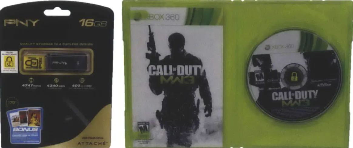
The lock design is highly dependent on key product features that can be used to render the product unusable. At the time of this project, locks have been designed for two product lines: USB thumb drives and CD-type disks (Figure 1). For the USB thumb drives, the lock is attached to the male plug. An improper attempt to remove the lock will permanently damage the plug, rendering the thumb drive useless. For the disks, the lock secures the disk to its case. Here, improper removal will simply break the disk or the packaging. In both scenarios the disk and packaging are not separated. The lock was designed so that the case or disk would break before the lock, which joins the two.
ProTeqt has developed several prototypes and working models of mechanical locking systems for a plethora of devices: from perfume to video games. A micro USB lock system will be analyzed throughout the extent of this thesis. This lock has been identified as a critical mechanism that will facilitate growth and opportunities for
ProTeqt, because the micro USB port is used on many different types of devices to both power, and transfer data.
Figure 1: The thumb drive lock (Left) and the CD-disk lock (right). Locking mechanisms are identified by the pad-lock symbol.
The current design for the micro USB lock uses a number of moving parts, including plastics, springs, and sheet metal encapsulated by an external plastic housing. Previously, ProTeqt's most successful lock has been a standard USB lock. This lock is substantially simpler, using only plastic to create the lock. The standard USB interface is much larger than the micro USB components, which also encourages a simpler design.
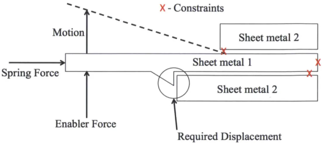
A simplified diagram explaining the interaction of the components inside the
micro USB lock is shown in Figure 2. We are limited in our discussion for purposes of confidentiality. The basic components inside the lock are the LC circuit (discussed in chapter 5), enabler, spring, and sheet metal components. For a product to be successfully unlocked, the enabler must produce a force inside the lock that bends a small sheet metal component. The sheet metal component (sheet metal 1) must be displaced until the small lip clears the second sheet metal component. At this point, a spring forces the first sheet metal component through the second, disengaging the lock. This displacement is
Sheet metal 2
Sheet metal 1Spring Force
Sheet metal 2Enabler Force
Required Displacement
Figure 2: Internal diagram of the micro USB lock system.
The enabler is the most important component in the lock. It expands when inductively heated (Chapter 2). The whole system depends on the enabler expanding enough to fire the unlatching device when it receives energy from the deactivation tablet. The basic dimensions of the full sized enabler are 12mm by 9mm, and about 0.3mm thick. Upon heating, the enabler can expand to nearly forty times its original size. The enabler consists of a polymeric material that is sandwiched between two sheets of metal foil. When on the tablet, the enabler intersects with lines of flux produced by the primary coil. These lines of flux generate eddy currents that inherently produce heat. When the parameters are correct, it's this heat that forces the enabler to expand, exerting a force on the other components in the lock.
1.3.3 Improving Product Performance
ProTeqt has complete control over their mechanical locking device and
deactivation tablet, but they must be compatible with many types of locking methods (eg.
USB, disk, etc.) and packaging. In the case of the USB thumb drives (Figure 4) and the
disks, the packaging is very slim, allowing the lock to be close to the deactivation tablet. Once the magnetic field is created, the lock is easily deactivated. Products that are embedded in thicker packaging (Figure 3) have proven to be more difficult to unlock because the magnetic field degrades rapidly with distance. ProTeqt has begun to
investigate solutions that will permit deactivation of the mechanical lock at a distance of 1 inch from the tablet.
ProTeqt, having developed two unique applications for their technology (USB tumb drive, and CD-type disk), is ready to move forward with the development for a, new, Micro USB lock. This lock will perform similarly to the USB thumb drive lock, in that it will interface with the consumer product internally. The Micro USB port uses a smaller profile than the standard USB port, introducing some new design challenges. However, the Micro USB lock is used far more prevalently and with more expensive products than the standard USB. Moving forward, ProTeqt would like to achieve the functionality of the Micro USB lock at 1 inch above the tablet surface.
Figure 3: External hard drive with thick packaging requires a stronger field. This packaging, being targeted by ProTeqt, leaves the lock at 1 inch above the tablet.
Figure 4: USB thumb drive packaging. Because the packaging is thin, the lock is very close to the primary coil and deactivation is easy.
1.4
Induction Heating
The most important concept of ProTeqt's current design is induction heating. They use this phenomenon to generate heat inside the lock; thereby causing a polymeric material to expand, which in turn creates a force that disengages the lock from the product. The principals of induction heating are applied from the tablet to the enabler. To simplify things, the tablet can be thought of as an induction cook top, and the enabler a pot. The main purpose of the deactivation tablet is to heat the enabler. More
information on induction heating is discussed in Chapter 2.
1.5
Resonant Coupling
As stated above, the objective of ProTeqt is to achieve unlocking at one inch from the tablet. Among several potential solutions, ProTeqt chose to explore and implement the effects of resonant inductive coupling. Resonant inductive coupling is a means to transfer wireless energy through two coils that are tuned to resonate at the same frequency. We can effectively use resonant inductive coupling to extend the magnetic field created by the deactivation tablet. In reality we can create a new magnetic field
using the energy transferred wirelessly from the original field created by the tablet. Using a field that is closer to the mechanical lock will increase the effectiveness, and decrease the decaying effects of the field at distance. Furthermore, this solution will allow ProTeqt to postpone a redesign of the deactivation tablet. Instead, a simple
component can be designed that will allow the wireless transfer of energy: an LC circuit.
1.6
Design and Production of LC Circuits
To extend the field, we need to develop an LC circuit. An LC circuit is a circuit comprises an inductor and a capacitor. This circuit is typically drawn as shown in Figure
5. By placing the small circuit inside the mechanical lock, we can create a new magnetic
field inside the lock. Although an LC circuit is simple (an inductor coil connected to a capacitor), it should be designed to work at maximum efficiency. The circuit can be tuned to operate most efficiently at a certain frequency. However, because the LC circuit will be operating inside the mechanical lock, we must consider the interaction and effects of the existing components of the lock. Moreover, the performance of the circuit is
dependent on the quality of manufacturing. Thus, the effects of manufacturing variability must be understood, controlled, and minimized.
L
1C
_T
Figure 5: Typical diagram for an LC circuit where L is the inductor and C is the capacitor.
Finally, because the circuit is inside the lock, it is disposable and must be
per year. The production rate and cost are two important parameters that must be considered and accounted for in the beginning stages of the design.
1.7
Problem Statement
The problem statement developed by ProTeqt for our thesis project was to understand the interactions between the deactivation tablet, LC circuit, and mechanical lock to optimize and, moreover, recommend a final design of the LC circuit that will excite the enabler at 1 inch above the tablet, thereby disengaging the lock, at a manufacturing cost of $0.05.
Building on this problem statement, the goal of the project is to develop an LC circuit that will effectively extend the application of ProTeqt's benefit denial solution from zero to one inch using resonant inductive coupling. Furthermore, the forces and interactions between the LC circuit, enabler, and mechanical lock were understood to provide a better understanding of ProTeqt's entire benefit denial solution. Multiple challenges were addressed, from theoretical physics to manufacturing issues. This thesis considers the topics we faced while working at ProTeqt. It must be noted that some tasks were distributed among ProTeqt's partners and are out of the scope of this thesis.
This project was conducted through three phases. In the first phase we worked to understand, characterize, and recommend and optimal design for an LC circuit to permit the transfer of wireless energy. For this phase it was necessary to understand the principle of induction heating, the physical mechanisms required to create a new magnetic field, and the parameters for optimizing the design of an LC circuit.
In the second phase, the unlocking mechanism was analyzed to understand the interaction between the mechanical parts and the circuit. The purpose of this stage is to obtain and understand data related to the forces required to disengage the locking mechanism.
Finally, in the last phase of the project, the effect of manufacturing variability and the variability of the components in the lock were analyzed to understand the likelihood of failure and the likely source of these failures.
1.8
Task Division
Based upon the three phases of the approach, tasks were divided among the three group members: Amaury Rony, Tianyu Zhu, and myself. Even though the thesis project at hand has been completed by the collective group, each team member took the lead on one of the three phases, and delegated the responsibility for tasks essential for completion as needed. Theoretical physics and coil design was under the responsibility of Amaury. I led the work on the unlocking mechanism and its interaction with the LC circuit
including the forces acting on and required by the lock. Finally, Tianyu took responsibility of the manufacturing variation.
Chapter 2
Induction Heating
2.1
Principals of Induction Heating
Induction heating is a method to heat an electrically conducting object using electromagnetic induction. An induction heater consists of an inductor excited with an alternating current. According to Faraday's Law, the changing current creates a changing electromagnetic field around the inductor. When the electrically conducting object is placed inside this field, eddy currents are generated within the conductor. This phenomenon causes Joule heating owing to losses in the conductor. Compared to traditional heating methods, induction heating does not require direct physical contact because the energy is transferred from the heater to the conducting component through electromagnetic waves.
2.1.1 Eddy Current
French scientist Francois Arago first discovered Eddy currents in 1824 [3]. When a conductor is placed in a changing magnetic field, circulating eddies of current are created inside the conductor. The name eddy current is derived from the analogy of circulating water in fluid dynamics. In a non-zero resistivity conductor, the eddy current induced will generate heat, by the concept of Joule heating, and electromagnetic forces. The current induced is greater with either a stronger magnetic field or a higher frequency magnetic field. According Lenz's law, the eddy current will flow in a direction such that the magnetic field created by the current will oppose the magnetic field that induces the current. In other words, the eddy current will create a lesser magnetic field that will cancel part of the primary field.
2.1.2 Skin Effect
In direct current, current density is uniform throughout the entire cross section of the conductor. Alternating current is different. The magnetic field at the center increases as the frequency increases due to the combined effects of conductivity and permeability. The magnetic field creates current in the opposite direction of the current flowing through the conductor, making it more difficult for the current to flow through the center. This resistance is called reactance. Because of the reactance at the center, the current density is the lowest there and largest near the surface of the conductor where the reactance goes to zero. This concentration of current at the surface is named the "Skin Effect".
Lw
t
ti
t t
Figure 6: Schematic of current and magnetic field in a conductor with alternating current. I (red arrows) is the current passing through the conductor. It induces the
magnetic field H (blue loops), which itself creates the loops of current, Iw. The AC current density decreases exponentially with the depth from the surface. The skin depth is defined as the distance into a conductor at which is current density falls to 37% of its value along the surface. The skin depth can be expressed as:
1
where:
f= frequency, t= absolute magnetic permeability of the conductor = o* pr,
[= Permeability of air = 4Tr * 10-7 Q), r = Permeability of the conductor
a = Conductivity of the material
For example, a copper wire with AC of 220 kHz, will have a skin depth of 0.141mm. This means that 63% of the current flowing in a copper wire will flow within a distance of 0.141mm to the surface. The effective resistance can be calculated as current flowing uniformly through a layer of thickness 6 with the DC resistivity of that material. The cross-sectional area can be approximated by [4]:
Aeff = 2rr - 8 (2.2)
where: r = radius of the wire Then, the AC resistance is:
r
RAc RDC (2.3)
All the equations shown above are based the assumption that the skin depth is
significantly smaller than the radius. By negating this assumption and using a wire diameter on the same order as the skin depth, a resistance at low frequency can be calculated using the following model:
Riow freq Rdc + 4862 (2.4)
where:
I = total length of the wire
To maximize the heating effectiveness, we want to find a proper combination of material properties and material thickness. Optimal heating can be achieved by
minimizing the material thickness to a value close to the skin depth.
2.1.3 Selection of Materials and Thickness
The selection of material is critical, because material properties determine the effectiveness of the energy transmission and subsequent heating. Only conductive
materials can be used for induction heating because eddy currents need to flow through the object in order generate heat. Even though eddy currents can occur in any conductor, iron and its alloys respond better than aluminum and copper to induction heating owing to their ferromagnetic nature. Using the same alternating current, ferromagnetic materials have a significantly smaller skin depth, resulting in greater resistance and therefore Joule heating.
For materials that are thinner than their skin depth at the desired frequency, the skin effect is no longer important. The resistance of the material is only determined by the thickness and basic material resistivity. In this case, aluminum and copper can perform just as well as ferromagnetic materials.
Chapter 3
Resonant Inductive Coupling
3.1
Magnetic Field Generated by Current
This section provides an initial background on electromagnetic theory. Based on this introduction, inductive coupling is introduced. ProTeqt uses a large electromagnet in the deactivation tablet to unlock their locks. To extend their deactivation distance from the surface of the tablet to an inch above, resonant inductive coupling has been
introduced to the system to permit efficient wireless energy transfer. For more extensive information, the reader can refer to a more detailed handbook like [4].
3.1.1 Magnetic Field Strength at a Coil Axis
Every current, i.e. a flow of moving charges, is associated with a magnetic field with magnitude that is represented by the magnetic field strength, B (in Teslas). The magnetic field generated by a line of current within a wire is derived from Biot-Savart law [4]. That is L-BQ = dlxi* (3.1) 4Q4 r JQp2 0 Where:
Q
is the point of observation.P is the center of the elementary element dl.
I indicated the intensity and the direction of the current at P. iq5j is an elementary vector from
Q
to P.p = Ir po is the permeability of the medium
From this equation, it is possible to find the magnetic field along a single circular loop of radius a, carrying a current I. We are especially interested in the magnetic field B, along the axis of the loop. It is oriented in the axis direction, as shown on Figure 7:
cizz
Figure 7: A current-carrying loop and it's associated magnetic field along the central axis.
The magnitude of the field is
Bz = = pa 3 (3.2)
2(z 2 + a2)2
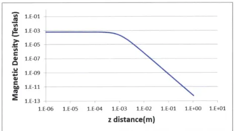
To understand the effect of distance, the magnetic density is plotted as a function of the distance from the hoop (Figure 8), which is a plot of equation 3.2 with a= 1 mm and 1=1. A 1.E-01 -4A W .E-05 . 1-09 ba 1.E-11 1.E-13 -
---1.E-06 1.E-05 1.E-04 LE-03 1.E-02 1.E-01 1.E+00 1.E+01
z distance(m)
Figure 8: Magnetic Field along the hoop axis, vs. the hoop radius (log-log scale). Hoop radius a= 1 mm and current I is 1 A in eqn 3.2.
As long as the distance from the conductor is less than the radius, the magnetic field remains approximately constant. However the magnetic density decreases rapidly as the measuring point is moved further away from the center of the loop.
As will be discussed below, a flat spiral coil can be used to increase the magnetic field by increasing the number of hoops. A spiral coil can be seen as a certain number of concentric hoops with different radii (a,, a2, a3... ), and potentially with N layers. In this
case, the total intensity of the magnetic field along the axis of the coil is the superposition of the magnetic field intensities generated by each single loop [5].
3.1.2 Magnetic Flux and Inductance
The line along which the magnetic strength is constant is called a line of magnetic flux. We are interested in the total magnetic flux, i.e. the total number of flux lines passing through a given surface. The magnetic flux cP is proportional to the field density B and the area:
P = B.A (3.3)
Going back to the current-carrying hoop, it is now possible to define and calculate its inductance L.
L =(3.4)
where cP is the magnetic flux through the inside surface of the loop.
L 1m (3.5)
2
It is noticed that inductance does not depend on the current. Equation 3.5 comes from the RFID handbook [5]. It only depends on the material properties and the
geometry layout. The inductance of a spiral coil is the sum of the inductances of each single hoop.
3.2
Inductive Coupling
If a second conductor hoop is located closed to the first one, a portion of the
magnetic flux (D21 from the first hoop passes through the second. The two conductors are
now inductively coupled. As for inductance (also known as self-inductance), we define the mutual inductance M21 of conductor hoop 2 in relation with conductor hoop 1 as:
(21
M = 111 (3.6)
In a similar way the mutual inductance of conductor hoop 1 in relation with conductor hoop 2 is:
M12 =
12 (3.7)
It has been shown that both mutual inductances are equal [5] i.e.
M12 = M2 1 = M (3.8)
Continuing with these two coils, we consider the case where the first inductor carries a high frequency, producing a varying magnetic field at the same frequency. With the secondary coil located in the surrounding area so that the two are coupled, Faraday's law states that any change to the magnetic flux generates an electric field, which induces a voltage in the secondary coil. It's this induced voltage that can be used to supply power to another application (RFID chip, transfonner, etc.).
3.3
Resonant Coupling
Experience and analysis [6] show that coupling decreases very quickly as the distance between two coils increases. To combat this issue, we add a capacitor to the circuit. This creates a resonance phenomenon that increases the coupling efficiency at a certain frequency. At this frequency, called the resonant or natural frequency, the power
transmission is much more efficient. Thus, the distance between the coils can be substantially increased.
3.4
Applications
The physical phenomena discussed in this chapter can be advantageously used for contactless electronic application. Two of the most important and applicable applications are RFID tags and wireless power. Both applications are used by ProTeqt. Before the deactivation of the lock, the product is recognized by its RFID tag, inside the package. Then, the principles of wireless power transmission will be used in order to increase the maximum distance of deactivation.
3.4.1 RFID
Today many companies, large and small, use automatic identification systems, or Auto-ID, for a large range of applications; including inventory management, sales and purchase, payment, safety controls, communication, and other means. The most widely used technologies in this field are the barcode and the smartcard scanning. Among all other available solutions, RFID systems (Radio Frequency Identification) have three major advantages: identification is passive, contactless, and reconfigurable. Like smart cards, data is stored on an electronic data-carrying device, called the chip. However, RFID devices do not require physical contact between the chip and the reader. Instead, data is exchanged with an electromagnetic field. Electromagnetic waves are emitted and received through two coils, or antennas. One is connected to the chip and the other one in the reader. The chip, when accompanied by the coil, is called the transponder.
To maximize the power transmission, and the working distance between the transponder and the reader, the resonant frequency of the system is used to convey information. Two types of transponders exist today: passive and active transponders. A passive transponder does not provide energy and, instead, receives it from the reader's magnetic field. This energy causes an impedance change of the transponder: shifting the initial natural frequency of the system, which is detected by the reader. Active
energy source. The signal is sent either periodically or in the presence of an RFID reader. Passive transponders are more widely used because they are less expensive, whereas active transponders are used in long distance applications [5].
3.4.2 Wireless Power
Wireless energy transfer is as old as alternating current [7]. The transformers that are ubiquitous in most electronic devices and indeed in all electricity distribution network transfer energy by using mutual inductance. In recent years wireless energy transfer for an array of application is quickly becoming an important use of resonant inductive coupling. A team of MIT physicists, and many others have been working on this subject
[8][9]. They realized that resonant objects tend to couple, as opposed to off-resonant
interaction, where their interaction remains extremely weak. Thus, energy transfer efficiency between two resonators increases based on the coupling level between them. This phenomenon is called non-radiative wireless energy transfer. Non-radiative energy transfer is much more interesting than other solutions, such as radiative transfer or directed radiation modes because, respectively, they produce a huge energy loss or require line of sight between transmitter and receiver. Some foreseen applications for non-radiative wireless energy are:
" Charging portable electronic devices by placing it within the source field e Supplying power to mobile robots and machines in a factory
* Supplying power to internal medical device (pacemaker, medicine delivering devices, etc.)
Several designs have been tested and refined. Currently, the highest efficiency is achieved with a four-coil apparatus: the power supply with an inductor, first resonator, second resonator, and the receiver with the device to power (light bulb). A schematic of the system is given in Figure 9.
I -
ci
(2 I I l4 1 R1 ML TX Helix Source(AC) RX Helix RLFigure 9: Typical strongly coupled magnetic resonance (SCMR) system. TX is the transmitting helix. RX is the receiving helix. [10]
In this configuration resonant inductive coupling only takes place between the two resonators. The transmitting helix is inductively coupled with the source loop. Similarly, the receiving helix is inductively coupled with the load loop. With this system, several promising achievements have been made including more than 90% efficiency at
15 cm distance, 40% efficiency with a single receiver at 2 m, and 60% efficiency with
multiple receivers at 2 m. Recently, the research team, now an MIT spin-off company called Witricity, introduced a repeater to further increase the effective distance of the magnetic field, and thus increase the transfer distance even further by inserting another set of resonators between the two previous ones (transmitting and receiving helixes). Ultimately, the work done at MIT is similar to our project, in that we want to extend the range of a magnetic field via resonant coupling. [9] [10] [11].
f, f2
Chapter 4
LC Circuit Manufacturing
ProTeqt had previously determined that an LC circuit with a resonant frequency near 220 kHz would be necessary for distance activation. This circuit would be part of each device, and therefore must be compact enough to fit in the locking device and inexpensive enough to keep the device cost low. These requirements make the design and manufacture of this circuit critical to the success of this product. In this chapter we examine a variety of methods for making such a device.
4.1
Introduction to the LC Circuit
As mentioned in the previous chapter, there have been many experiments and tests in the wireless energy transfer design space. ProTeqt had done preliminary research to explore the design space, and found that the performance achieved by the LC circuit could prove feasible for extending the working distance of their locks to one inch. The
LC Circuit can be thought of as a passive receiver. That is, the LC circuit does not
contain a battery or any other power source, nor does it require its own power source to receive a signal. LC circuits can be manufactured at a very low cost because they do not contain a power source.
An LC circuit only contains an inductor (L) and a capacitor (C). Thus, manufacturing is rudimentary. One must simply join an inductor and capacitor to complete the circuit. Based on the inductance and capacitance of the two components, the natural frequency of the circuit can be predicted with the following equation:
1
f 2 L (4.1)
This leaves two variables that can be changed with respect to each other, in order to achieve a certain natural frequency. The most efficient transfer of wireless energy occurs when the transmitter, or deactivation tablet, emits an electromagnetic field at the natural frequency of the LC circuit. It's here that ProTeqt would like to be in the design -- -- - --- ... .. .... .... I'll, ... ... - -- -- -- -- --- --- . ....
4.2
Inductor Manufacturing
An inductor, in its simplest form is a coil of wire used to resist an electrical current change [12]. A conductor resists motion of an electrical charge; an inductor resists current flow based on self inductance. The coil of wire stores energy in a magnetic field created by current flowing through a coil. Inductors come in many shapes and sizes. These parameters often affect inductor performance [13]. The magnetic field created by an inductor is dependent on inductor shape, whereas the intensity of the field is
determined by the number of turns within the coil. For our application we are interested in designs that will permit an electromagnetic field extension through resonant coupling. Materials are especially important in inductors. The time required to establish a magnetic field is proportional to the coil resistance [12]. High current is desirable to quickly set up a magnetic field. Changing the linear length of the coil, or the coil's material properties can alter resistance, and therefore the field [13]. High coil resistance will also result in heating, and therefore promotes energy loss.
For this project, three inductor-manufacturing methods were analyzed: chemical etching, coil winding and screen printing. After consulting ProTeqt's manufacturing partner, MeadWestVaco, winding is currently the cheapest method to make coils quickly and in a repeatable fashion. However, other methods may be considered for two reasons: * If they can achieve better energy transmission between the primary and secondary
coils, or
* If they become more competitive in the near future.
4.2.1 Chemical Etching
Chemical etching is a controlled material removal process that uses a resist to prevent portions of a material from being removed by a chemical etchant. Once the resist is removed, a desired pattern remains (Figure 10). The process at hand uses copper and a resist to etch a copper pattern.
Before Etch Resist Copper Laminate Resist Copper Copper Laminate
Figure 10: Schematic of a typical etching process.
Figure 10 explains how chemical etching works [14]. You will notice that the etchant removes material in two directions, not just vertically. That is, a slight angle is apparent in the final product because the etchant is in contact with that portion of the material after it passes beyond the resist. Finally, it's important to not that this is a chemical material removal process. Meaning the copper that is removed cannot be easily recycled, making the process as a whole, inefficient.
Etching allows for batch processing of inductors however, it restricts coil designs to single layer, flat spiral coils. Economical etching is usually done in large batches of very thin materials. These materials are often on the order of 0.03mm thick [14]. As material thickness increases, time to etch increases. This property is inefficient in terms of processing energy. This directly impacts the production cost.
As material thickness decreases, resistance increases. This resistance restricts current flow through the material, and therefore increases the amount of voltage needed to create an electromagnetic field. The time requirement to etch thick pieces of copper
(0.5mm) is about 5 minutes [15]. This however is not what limits the chemical etching
process in terms of this application. The limiting factor is in the material costs. Copper is very expensive, and is only one of the materials used in the process. Resist and the chemical etchant also need to be purchased, along with the many cleaning solutions used to remove the etchant.
4.2.2 Coil Winding
Coil winding is a process that bends a wire (usually radially) into a desired shape. This can be done manually or automatically, and many different winding patterns can be achieved. This process bodes well for inductor manufacturing because an inductor, in its most basic form, is a wound coil. Size and shape of the coil, and wire used to create the coil can impact the inductor performance. Wound coils can be formed into almost any desired shape including flat spiral, cylindrical, rectangular, etc. Wire geometry is often limited by market availability. Rectangular and circular cross sectional wire are most common. Wires are found most commonly in certain AWG gage sizes, which have a circular cross section. Diameters are fully customizable depending on the type of winding machine. Usually machines can operate using a range of wires. Automatic machines often integrate several functions including dispensing, winding, and cutting the wire. Machines can accommodate simultaneous coil winding, providing a batch process. Batch processing allows the machines to produce coils at a high rate.
The cost of wire is extremely cheap [16]. Wire is packaged as a large spool that is fed into the coil winding machine. Because the wire is continuous, there is almost no waste and the two ends of each coil are left exposed, ready to be soldered to the remaining capacitor.
4.3
Capacitors
Capacitors are common electrical components used in many types of circuits. They consist of two conductive plates that are separated by a dielectric layer. This configuration allows capacitors to hold a charge. Capacitors come in many shapes and sizes for different applications (Figure 11). Capacitors are made in extremely high volumes by expert manufactures. With their cost at $0.0074 / capacitor2, ProTeqt will be
purchasing capacitors to use within their circuit.
Figure 11: Typical shapes and sizes of capacitors.
Capacitor specifications usually include three key pieces of information: nominal
capacitance and rated voltage. A capacitor will likely have these values printed on its side. A capacitor reading 1 pf 20% at 1 00V, for example, will have a nominal
capacitance of 1 microfarad with a tolerance of± 20% (0.8pf - 1.2pf). Throughout the life of the capacitor, it should not handle more than 100 volts, as that is the rated voltage.
4.4
Soldering Techniques
Soldering is a method ofjoining two thin metals using a filler material. This filler material has a lower melting temperature than the two thin metal pieces, allowing the filler material to flow between, and bond to each of the thin metal pieces. The filler material is often made of tin and lead. Conductive properties allow soldering techniques to be prevalent in the electronics manufacturing industry, and especially circuit board manufacturing. Two common soldering methods are used in manufacturing today: robotic soldering and dip soldering.
Robotic soldering often uses a robot or other automation to control temperature and the feed rate of the filler material. Sophisticated control systems are used to gain a high level of precision over soldering processes. Robotic soldering often requires auxiliary tooling or methods of positioning and orienting components before they can be soldered.
Dip soldering is used more extensively for circuit board manufacturing. This process is used to solder several components simultaneously. Leads from electrical components protrude through the bottom of the printed circuit board. These are dipped into a lead-tin bath, where the solder then solidifies upon removal. [17]
4.5
Screen Printing
Screen printing is a highly integrated manufacturing process that can provide an entire LC circuit in one process. This means that it can produce the inductor and the capacitor in one process. The process uses a mask that contains the circuit pattern. Conductive ink is then deposited on the mask, and the circuit is printed on the areas not protected. Silver and Aluminum are the most popular conductive inks used in this process. Dielectric materials can also be used to print capacitors. This is done in layers. First a silver layer is deposited, followed by a dielectric, and finally another silver layer.
[18]
The flexibility of screen printing is similar to that of chemical etching. It is commonly used for making flat, flexible circuits. The deposited layers are very thin (40 micron), but can be built up in layers. Building layers requires more processing time, and is therefore less economical. The thin nature of screen printing causes inherently high resistance values. Capacitors are printed as large flat surfaces, requiring a large amount of surface area. Spacing is also critical in screen printing. The silver ink does not have an insulating coating, so line spacing also requires more space. Like chemical etching, large batches can be printed at once. However, screen printing requires no post
processing because the capacitor can be printed as part of the circuit. [18]
The screen printing process is relatively new when compared to processes like etching or winding. While the added flexibility and integrated components are great for circuit board design and manufacture, it is still a new processes, and therefore costly. Even at the materials level, silver inks are much more expensive than copper for a given volume. While this process isn't right at this time, future developments could lead to significant cost reduction, leaving it as a potential process for future manufacturing. [18]
4.6
Manufacturing Recommendations
As stated above, three manufacturing methods; winding, etching and screen printing were chosen to conduct a preliminary comparison. The manufacturing analysis is based on three criteria: design feasibility, cost, and manufacturing feasibility. For more information on this topic, please refer to Tianyu Zhu's thesis [19].
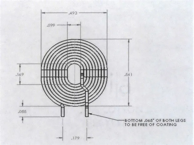
Engineers at ProTeqt had been successful using a hand made wound coil. The coil was made of AWG 24 copper magnet wire, with 9 turns. It had an oval shape to maximize its surface area. The hand wound coil was created to mimic the coil shown in Figure 12.
Among the three potential manufacturing methods, winding is the most straight forward, and cost effective. Being that the existing coil was hand wound, there is a high variability associated with the manufacturing method. Producing wound coils of the same dimensions by machines would prove to be more repeatable, especially in terms of inductance. The length of wire would be very consistent, providing a repeatable
resistance in the copper wire. For etching and screen printing, however, the resistance of the coil is significantly higher due to the very thin nature of the processes. Metal foil used in etching is normally thinner than 0.1mm. Thicker foil will increase cost and the
manufacturing time. The thickness of a screen printing pattern is normally below I 00pm. Multiple-layers are feasible, but just as with increasing the thickness of foil in etching, it will raise both cost and process time.
In addition to the design challenge, the manufacturing cost of etching and screen printing is higher than winding. Etching, being a fairly complicated process, requires higher equipment cost, includes a complex procedure, and has more material waste than winding. For screen printing, the cost of ink alone is higher than $0.05. Taking all the factors into consideration, winding was the manufacturing process chosen to perform future design optimization and analysis. Again, for a more detailed manufacturing cost analysis and further information on the decision to use wound coils, please refer to Tianyu's thesis [19].
169 .493 .099
.085
i
.19 .54BOTTOM .065" OF BOTH LEGS TO BE FREE OF COATING
Figure 12: Example of a hand wound coil design.
... -- ----- -- . ... . .... ..... .... ... ..... . ... ...
Chapter
5
Coil and Circuit Design
5.1 Objectives and Design Constraints
The objective of this section is to provide an optimized design of the LC circuit after understanding all of the constraints, whether set by ProTeqt or inherent in the manufacturing process of the coil. For a more detailed analysis of coil design please see Amaury Rony's thesis [20].
R C CTYP
1161
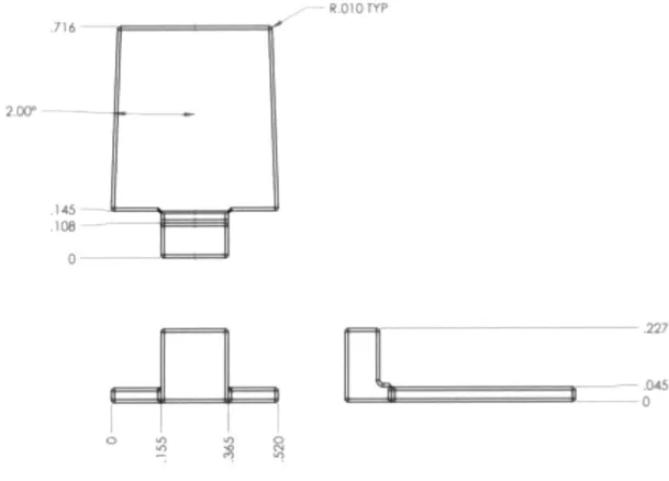
Figure 13: Usable volume (in inches) inside the lock, dedicated for the LC circuit.
As previously discussed the LC circuit at hand will be designed as a passive receiver that will extend ProTeqt's unlocking capabilities to one inch above the tablet. The two components of the circuit are the inductor and capacitor of, which, the inductor provides the most freedom in terms of design. The circuit design must consider several constraints. First, the circuit must comply with the existing design for the micro USB
lock. ProTeqt has designed the external housing with an opening in which the circuit must fit. This introduces geometric constraints. The circuit must not exceed a diameter of 12.74 mm, and should be less than 1.143 mm in height (see Figure 13). Other constraints include functionality at an inch above the surface of the tablet and manufacturing cost at less than $0.05.
5.2
LC Circuit Experimentation
The inductor and capacitor share a relationship that can be optimized in order to create the most effective field, thereby heating and expanding the enabler. The most important design component is the inductor because it must act as an antenna and
generate it own field. The inductance depends on the geometry of the coil. the wire gage size and number of turns in the coil. Once the inductor has been optimized in terms of gage size and turns, a capacitor can be chosen to target a certain natural frequency for the circuit.
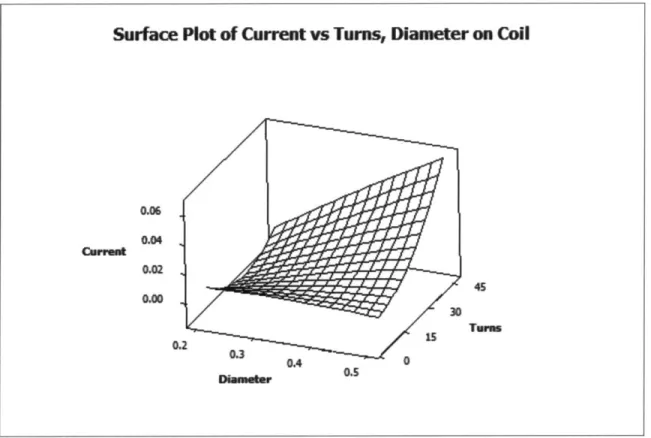
To find the optimal inductor geometry a design of experiments was conducted to generate a response surface based on the wire gage and number of turns in the coil. The measured output of this test was voltage, which was converted to current based on the known resistance of the coils. To conduct the experiment a primary coil was connected to a function generator and amplifier and placed below a surface representing the deactivation tablet. Above this setup, six different circuits with different inductor geometries were connected to an oscilloscope in order to measure the peak-to-peak voltage. From here the values were converted into current using the known resistance and inductance values of the coils To maximize the field generated by the inductor, the current in the coil should be maximized. This will create a strong magnetic field, providing the maximum amount of eddy currents used to generate heat in the enabler.
The deactivation tablet has been optimized to operate around 220 kHz. To operate around this natural frequency we measured the inductance of each coil, and then paired it with the proper capacitor. After generating the response surface, the inductor
geometry was optimized based on the geometric lock constraints. The capacitor was then selected based on the optimal geometry. The pairing of the two components lead to the optimal design of the LC circuit.
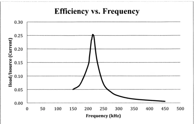
Using the optimal design, experiments were conducted to understand the coupling efficiency between the two coils. To measure the efficiency, voltage was measured in the primary circuit, and the LC circuit. The ratio of voltage measured in the LC circuit to the
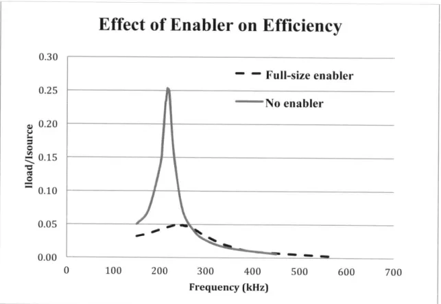
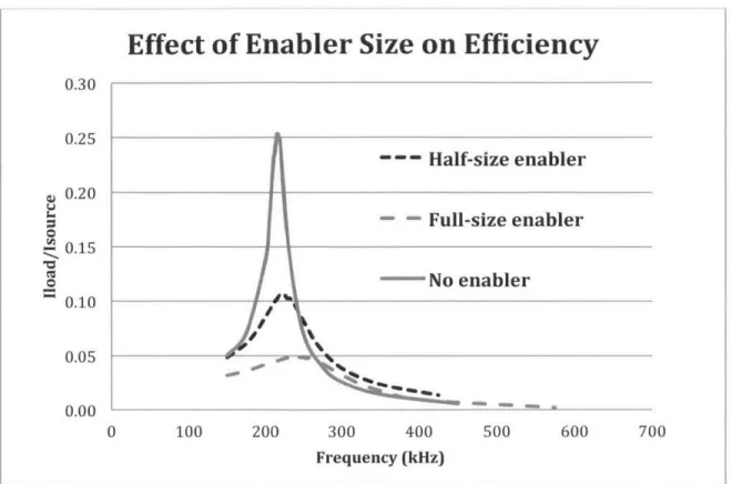
voltage measured in the primary coil was recorded with respect to frequency. Finally, using this method, the effects of placing the circuit inside the lock were analyzed to understand the effect of the lock on the efficiency of the coupling between the primary coil and the LC circuit.
5.3 LC Circuit Optimization and Test Results
The inductor and capacitor share a relationship that can be optimized for the most effective field, thereby heating and expanding the enabler. The most important design component is the inductor because it must act as an antenna and generate its own field. The inductance depends on the geometry of the coil. The inductance will change with the wire diameter and number of turns, especially considering that we are making flat spiral coils: as the number of turns increases, the diameter of the coil as a whole increases, therefore allowing it to intersect with more lines of flux from the primary coil.
As we tested our six coils of varying gage size and number of turns, we gathered data and generated a response surface that would help us to predict the performance of any other combination of gage sizes or number of turns. The response surface can be found in Figure 14. From this surface we see that the wire gage and number of turns in the coil should be maximized to generate the most current. Intuitively we would want a larger gage size to reduce the resistance and thereby increase the current. Also, increasing the wire gage corresponds to a shorter wire. If we had two coils that had the same outer diameter, but different gage sizes, the larger gage size would have a shorter unwound wire, which again decreases resistance and increases current flow.
With a general understanding of how current corresponds to a coil design, other constraints were considered in order to fully optimize the circuit. It was found that the largest gage size that could fit within the given allowable volume of the lock was AWG 24. This wire diameter is around 0.5 mm. This is the maximum gage size because the wire must be routed in and out of the flat spiral coil, making the coil thickness at least
the wire gage in place, we calculated the maximum number of turns that would fit in the cavity to be 9, when leaving an appropriate inside diameter for the manufacturing of the coils. A theoretical model was created to confirm this design. Table 1 shows the optimal coil using the theoretical model. The output of the model is current. For more on the theoretical model, please see Amaury Rony's thesis [20]. From the table we again gather that optimal design for the inductor coil uses 24 AWG wire for a coil with 9 turns.
Figure 14: Response surface in current for various coil characteristics. Surface Plot of Current vs Turns, Diameter on Coil
0.06 0.04 0.02 0.00 45 30 Tuu 0.2 0s 03 0.4 .5 0