HAL Id: hal-02987332
https://hal.laas.fr/hal-02987332
Submitted on 10 Nov 2020HAL is a multi-disciplinary open access
archive for the deposit and dissemination of sci-entific research documents, whether they are pub-lished or not. The documents may come from teaching and research institutions in France or abroad, or from public or private research centers.
L’archive ouverte pluridisciplinaire HAL, est destinée au dépôt et à la diffusion de documents scientifiques de niveau recherche, publiés ou non, émanant des établissements d’enseignement et de recherche français ou étrangers, des laboratoires publics ou privés.
Performance Analysis of RL Damper in GaN-Based
High-Frequency Boost Converter
A Gutierrez, E Marcault, Corinne Alonso, David Trémouilles
To cite this version:
A Gutierrez, E Marcault, Corinne Alonso, David Trémouilles. Performance Analysis of RL Damper in GaN-Based High-Frequency Boost Converter. 22nd European Conference on Power Electronics and Applications (EPE’20 ECCE Europe), Sep 2020, Lyon (virtuel), France. �10.23919/EPE20ECCEEurope43536.2020.9215645�. �hal-02987332�
Performance Analysis of RL Damper in GaN-Based High-Frequency
Boost Converter
A. Gutierrez1, E. Marcault1, C. Alonso2, D. Tremouilles2 1CEA-Tech Occitanie
51 Rue de l’Innovation, Labege - France 2LAAS-CNRS
7 Avenue du Colonel Roche, Toulouse - France
Emails: [email protected], [email protected] [email protected], [email protected]
Acknowledgments
This work has been partially funded by the Region Occitanie Pyr´en´ees-M´editerran´ee.
Keywords
GaN-HEMT , Boost converter , RL damper , Root trajectory , Switching losses .
Abstract
This paper analyzes a high-frequency GaN-based boost converter considering an RL damper to mitigate critical oscillations. This work aims contributing with graphical correlations between power converter signals and root trajectories of the characteristic equation in the main oscillation loop. Results provide insights about the RL damper design to improve the power converter performance. A technical contribu-tion shows that the highest efficiency depends on the lowest L and the highest R of the RL damper able to produce a damping operation. Additionally, simulation results demonstrate the improvement of the GaN-HEMT operation and reliability using an RL damper in a boost converter topology. An experimen-tal GaN-based boost converter validates the developed study.
1
Introduction
Recent advances in Gallium Nitride - High Electron Mobility Transistors (GaN-HEMTs) have increased the switching frequency of DC-DC power converters at megahertz level. However, this high switching frequency also associates several design challenges [1]. For instance, GaN-based power converters at high-frequency are highly susceptible to unexpected current fluctuation and overshoot voltage [2]. In addition, the interaction of the parasitic inductance and the inherent capacitance of power semiconduc-tors lead to hazard oscillations at the GaN-HEMT terminals [3]. This increases the risk of false turn-ON and device failures [4]. As a result, these undesired oscillations in high-frequency trend to decrease the power converter performance and reliability [5].
Most common methodologies to decrease these oscillation issues search the minimization of the layout inductance [6]. However, Middelstaedt et al. argue that undesired oscillations in the megahertz band can still remain despite the minimized layout inductance [7]. Indeed, Yano et al. propose an optimiza-tion methodology for designing RL and RC snubbers to mitigate the impact of these oscillaoptimiza-tions [8]. Therefore, suitable methodologies are still required to analyze and design filter networks to decrease the potential hazard oscillations. Additionally, these filter networks should be able to increase the power conversion performance in high-frequency operation.
In this context, this work aims to contribute with an analytical and graphical approach to correlate the power converter signals against the root trajectories of a characteristic equation which includes an RL damping network. To achieve this goal, we analyze a high-frequency boost converter as study case. As a first step, boost converter simulations demonstrate that packaging parasitic inductances and inherent semiconductor capacitances are able to produce hazard oscillations for the GaN-HEMT device. Then, an analytical and graphical approach compares the power converter signals and the root trajectories of a simplified characteristic equation given RL damping parameters. Next, these comparison results lead to describe the interaction between the damping network and the power converter performance. After, the analysis of this interaction provide design criteria for the RL damper to achieve a suitable trade-off between mitigated oscillations and power converter efficiency. Finally, an experimental GaN-based boost converter validates the proposed approach under high-frequency switching conditions.
2
RL damper in a high-frequency boost converter
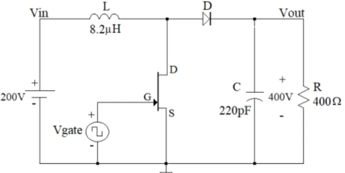
This section describes the studied RfLf damping network in a high-frequency boost converter. The study case is a GaN-based boost converter of 400V/400W/30MHz. The ideal case is shown in Fig. 1. In ad-dition, Fig. 2 depicts the parasitic elements considered by the analysis. The parasitic inductances are designated as Lps(total parasitic inductance source-side), Lpd (total parasitic inductance drain-side), Lpk (package diode inductance), and Lpt (layout parasitic inductance). The intrinsic semiconductor capaci-tances are Co(effective output capacitance of the GaN device), and Cpk(total diode capacitance).
Fig. 1: High-frequency boost converter based on GaN-HEMT - Ideal case.
Fig. 2: High-frequency boost converter based on GaN-HEMT with parasitic elements given by Co=17pF, Cpk=8pF, Lps+Lpd+Lpk+Lpt=3nH.
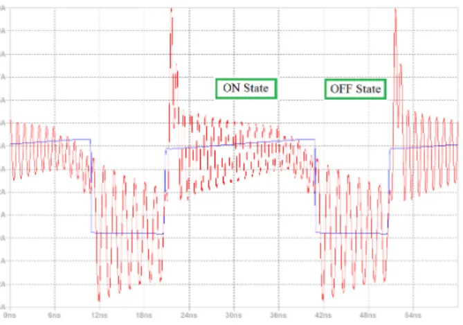
Figure 3 depicts the drain current of the boost converter for the cases ideal and with parasitic elements. In Fig. 3, the drain current presents significant oscillations despite the relative low parasitic inductance. Furthermore, Fig. 4 shows the current spectrum with oscillation frequencies in the ON and OFF states. As shown in Fig. 4, these oscillation frequencies are able to overlap the current spectrum for the ideal case without parasitic inductances.
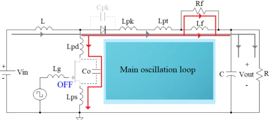
In order to decrease the impact of the parasitic elements, a RfLf damping network is included in the main oscillation loop. Figure 5 shows the current flow in the ON state considering the RfLf. Figure
Fig. 3: Drain current. Color nomenclature: blue - ideal case, red - with parasitic elements.
Fig. 4: Spectrum of drain current. Color nomenclature: blue - ideal case, red - with parasitic elements. 6 describes the current behavior in OFF state. Next section presents the theoretical analysis given this RfLf damping network in the main oscillation loop.
Fig. 5: GaNbased boost converter with RL damper ON state. Color nomenclature for current: gray -state steady current, red - transient current.
3
Characteristic equation of the main oscillation loop
This section develops the framework to analyze the main oscillation loop. Fig. 7 shows a simplified version of the main oscillation loop. This simplified circuit models the ON/OFF states by considering Cs as either Cpkor Co.
Fig. 6: GaNbased boost converter with RL damper OFF state. Color nomenclature for current: gray -state steady current, red - transient current.
Fig. 7: Simplified circuit version of the main oscillation loop. The Kirchhoff’s voltage law in the simplified circuit is given by eq.(1),
vCs + vLs + vF = 0 (1)
first derivative of eq.(1) is given by eq.(2), d vCs dt + d vLs dt + d vF dt = 0 (2) thus, i Cs + Ls d2i dt2+ dvF dt = 0 (3)
considering the current relation in the RfLf damping network, dvF
dt = Lf d2iLf
therefore, Lf d2vF dt2 + Rf dvF dt − LfRf d2i dt2 = 0 (5)
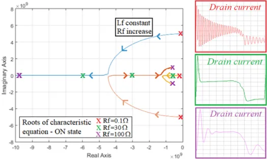
the characteristic equation for the i current in the main oscillation loop is given by eq.(6) solving the system of differential equations from eq.(3) and eq.(5) using Laplace transform.
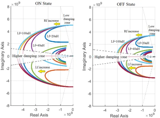
LfLsCss3 + (RfCsLf+ RfCsLs)s2 + Lfs + Rf = 0 (6) This characteristic equation describes the natural oscillations of the drain current in each ON/OFF -OFF/ON transition. The total current response depends on this natural response and the response in steady state. Figure 8 illustrates the root trajectories of the characteristic equation in ON state by con-sidering an Lf constant and increasing Rf. Figure 8 shows that root localization modifies drastically the drain current. As shown in Fig. 8, Lf constant and increased Rf displace the root trajectory from a highly oscillatory region near to the imaginary axis toward a more stable region close to the real axis. However, increasing excessively Rf can return again to an oscillatory region. Next section describes the relation between the current and voltage signals of the power converter with the root trajectories.
Fig. 8: Root trajectories of characteristic equation - ON state. Each colored square depicts the total drain current according to the root localization.
4
Correlation between power converter signals and root trajectories
This section presents the impact of the root trajectories on both the global converter performance and the switching device signals. As illustrative example, Fig. 9 depicts the root trajectories of eq.(6) by increasing Lf and Rf in both the ON and OFF states. The root trajectories in the low damping zone are wider for the ON state case. Therefore, higher oscillations are produced in the current drain signal as shown in the Fig. 10. In contrast, the root trajectories in the OFF state in the same low damping zone cause more moderate drain current signals (see Fig. 10). Additionally, the drain voltage is distorted by the root locations in the low damping zone. In the high damping zone, the root locations lead to more stable current and voltage signals. As a consequence, Fig. 10 shows the advantage for the GaN-HEMT operation in the high damping zone given the lower risk of potential hazard signals.
The analysis of the root trajectories of eq.(6) shows that the high damping zone can be achieved by a set of Lf and Rf values. Therefore, a criterion is required to achieved a suitable trade-off between signal
Fig. 9: Root trajectories for ON and OFF states
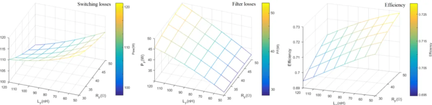
damping and power converter performance. To describe this trade-off, Fig. 11 allows comparing the influence of the Lf and Rf selection on the switching losses, the filter losses, and the power converter efficiency. Fig. 11 demonstrates that different Lf and Rf combinations in the high damping zone produce dissimilar conversion performance. The most remarkable result from Fig. 11 is that the highest efficiency depends on the lower Lf and the higher Rf able to produce a damping operation. Furthermore, this result also highlight the constraint of the RL damper in a boost converter because the lowest switching losses and the highest conversion efficiency cannot accomplish at the same time given the intrinsic nature of the analyzed damping network. Next section will introduced the experimental results.
Fig. 11: RfLf parameters of the high damping zone and power conversion performance. Switching losses (left), RL damper losses (center), converter efficiency (right).
5
Experimental high-frequency boost converter using an RL damper
A GaN-based boost converter at 400V/400W/30MHz is implemented to validate the proposed approach. Figure 12 shows the experimental setup of the implemented high-frequency boost converter compared with simulation results. Table I lists the experimental boost converter parameters with the RL damper in the main oscillation loop.
Table I: Parameters of experimental boost converter with RL damper Parameter Value Vin 200V Vout 400V Lf 56nH Rf 50Ω Pin 615W Pout 400W η 0.65 Fsw 30MHz Output Ripple 20%
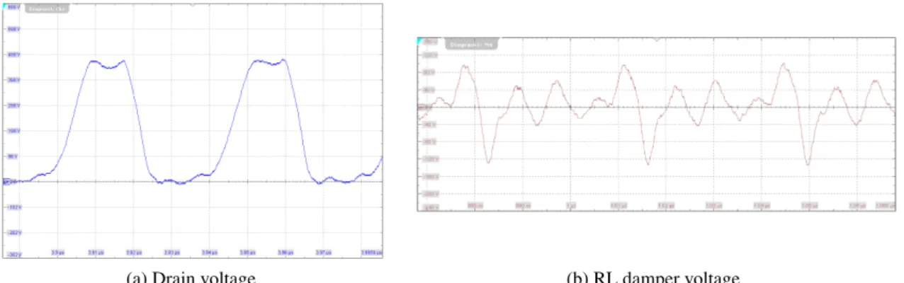
Figure 13 shows the drain voltage and the RL damper voltage. As shown in Fig. 13, the RL damper network absorbs the undesired oscillations which allows a normal operation of the switching device. However, the global efficiency of the power converter was approximately 8% lower than expected given other associated losses not included in the analysis.
(a) Drain voltage (b) RL damper voltage
Fig. 13: Drain voltage and RL damper voltage of experimental GaN-based boost converter.
6
Conclusion
This work studied the performance of a RL damper in a GaN-based boost converter at high-frequency. Results allowed describing the correlation between power converter signals and the root trajectories of the characteristic equation in the main oscillation loop. The incorporation of the RL damper demonstrated its potential to improve the converter efficiency and to decrease the critical oscillations. Additionally, This result demonstrates the improvement of the GaN-HEMT operation and reliability. A remarkable result showed that the highest efficiency depends on the lowest Lf and the highest Rf able to produce a high damping operation. However, this result also demonstrated that the advisable condition of lowest switch-ing losses and highest conversion efficiency cannot be accomplished usswitch-ing the RL damper. Therefore, device manufacturing and converter design efforts are still required to decrease the switching losses in high-frequency boost converters. An experimental boost converter validated the RL damper performance in a high-frequency boost converter.
References
[1] H. A. et .al, ”The 2018 GaN Power Electronics Roadmap”, Journal of Physics D: Applied Physics, vol. 51, 2018.
[2] K. Wang, L. Wang, X. Yang, X. Zeng, W. Chen, and H. Li, ”A Multiloop Method for Minimization of Para-sitic Inductance in GaN-Based High-Frequency DCDC Converter”, IEEE Transactions on Power Electronics, vol. 32, no. 6, pp. 47284740, 2017. DOI: 10.1109/TPEL.2016.2597183.
[3] K. Wang, X. Yang, L. Wang and P. Jain, ”Instability Analysis and Oscillation Suppression of Enhancement-Mode GaN Devices in Half-Bridge Circuits”, in IEEE Transactions on Power Electronics, vol. 33, no. 2, pp. 1585-1596, Feb. 2018, doi: 10.1109/TPEL.2017.2684094.
[4] T. Iwaki, T. Sawada, and M. Yamamoto, ”An mathematical analysis of false turn-on phenomenon
of GaN HEMT”, in 2017 IEEE CPMT Symposium Japan (ICSJ), 2017, pp. 189190. DOI:
10.1109/ICSJ.2017.8240113.
[5] L. Efthymiou, G. Camuso, G. Longobardi, T. Chien, M. Chen and F. Udrea, ”On the Source of Oscillatory Behaviour during Switching of Power Enhancement Mode GaN HEMTs”, in Energies 2017, 10(3), 407; doi.org/10.3390/en10030407
[6] T. Liu, T. T. Y. Wong, and Z. J. Shen, ”A Survey on Switching Oscillations in Power Convert-ers”, IEEE Journal of Emerging and Selected Topics in Power Electronics, pp. 11, 2019. DOI: 10.1109/JESTPE.2019.2897764.
[7] L. Middelstaedt, J.Wang, B. H. Stark, and A. Lindemann, ”Direct Approach of Simultaneously Elimi-nating EMI-Critical Oscillations and Decreasing Switching Losses for Wide Bandgap Power Semicon-ductors”, IEEE Transactions on Power Electronics, vol. 34, no. 11, pp. 10 37610 380, 2019. DOI: 10.1109/TPEL.2019.2913223.
[8] Y. Yano, N. Kawata, K. Iokibe, and Y. Toyota, ”A Method for Optimally Designing Snubber Circuits for Buck Converter Circuits to Damp LC Resonance”, IEEE Transactions on Electromagnetic Compatibility, vol. 61, no. 4, pp. 12171225, 2019. DOI: 10.1109/TEMC.2018.2841424.