HAL Id: hal-02341919
https://hal.archives-ouvertes.fr/hal-02341919
Submitted on 31 Oct 2019
HAL is a multi-disciplinary open access
archive for the deposit and dissemination of sci-entific research documents, whether they are pub-lished or not. The documents may come from teaching and research institutions in France or abroad, or from public or private research centers.
L’archive ouverte pluridisciplinaire HAL, est destinée au dépôt et à la diffusion de documents scientifiques de niveau recherche, publiés ou non, émanant des établissements d’enseignement et de recherche français ou étrangers, des laboratoires publics ou privés.
Optical Nanoimpacts of Dielectric and Metallic
Nanoparticles on Gold Surface by Reflectance
Microscopy: Adsorption or Bouncing?
Jean-François Lemineur, Talia Jane Stockmann, Jérôme Médard, Claire
Smadja, Catherine Combellas, Frederic Kanoufi
To cite this version:
Jean-François Lemineur, Talia Jane Stockmann, Jérôme Médard, Claire Smadja, Catherine Combellas, et al.. Optical Nanoimpacts of Dielectric and Metallic Nanoparticles on Gold Surface by Reflectance Microscopy: Adsorption or Bouncing?. Journal of Analysis and Testing, 2019, 3 (2), pp.175-188. �10.1007/s41664-019-00099-8�. �hal-02341919�
ORIGINAL PAPER
Optical Nanoimpacts of Dielectric and Metallic Nanoparticles on Gold
Surface by Reflectance Microscopy: Adsorption or Bouncing?
Jean‑François Lemineur1 · Talia Jane Stockmann1,2 · Jérôme Médard1 · Claire Smadja3 · Catherine Combellas1 ·
Frédéric Kanoufi1
Received: 9 February 2019 / Accepted: 22 March 2019 / Published online: 15 April 2019 © The Nonferrous Metals Society of China 2019
Abstract
Optical modeling coupled to experiments show that a microscope operating in reflection mode allows imaging, through solutions or even a microfluidic cover, various kinds of nanoparticles, NPs, over a (reflecting) sensing surface, here a gold (Au) surface. Optical modeling suggests that this configuration enables the interferometric imaging of single NPs which can be characterized individually from local change in the surface reflectivity. The interferometric detection improves the optical limit of detection compared to classical configurations exploiting only the light scattered by the NPs. The method is then tested experimentally, to monitor in situ and in real time, the collision of single Brownian NPs, or optical nanoimpacts, with an Au-sensing surface. First, mimicking a microfluidic biosensor platform, the capture of 300 nm FeOx maghemite NPs from a convective flow by a surface-functionalized Au surface is dynamically monitored. Then, the adsorption or bouncing of individual dielectric (100 nm polystyrene) or metallic (40 and 60 nm silver) NPs is observed directly through the solution. The influence of the electrolyte on the ability of NPs to repetitively bounce or irreversibly adsorb onto the Au surface is evidenced. Exploiting such visualization mode of single-NP optical nanoimpacts is insightful for comprehending single-NP electrochemical studies relying on NP collision on an electrode (electrochemical nanoimpacts).
Keywords Reflection microscopy · Single nanoparticle · Sensor · Adsorption · Silver · Polystyrene
1 Introduction
Many sensors rely on a recognition event often due to the interaction of an analyte with a sensing surface; electro-chemical sensors and electrodes are some of them. However, defects or domains of heterogeneous reactivity are often pre-sent on sensing surfaces impacting the overall sensor perfor-mances. As the sensors rely on a macroscopic measurement, such as a macroscopic current or potential response in the case of an electrode, it is crucial to be able to recognize
spatially their heterogeneous activity, while the sensing reac-tion is operating. In this respect, different electrochemical strategies are proposed to map and quantify localized (elec-tro)chemical activity of surfaces.
On one hand, the (electro)chemical activity of a sur-face can be mapped using scanning electrochemical probe microscopies (SEPMs) such as the scanning electrochemi-cal microscopy which uses a micro/nanoelectrode to map the electrochemical activity of a surface [1]. More recently with the scanning electrochemical cell microscopy [2], a nanodroplet is spread over a surface forming a micro/nano-sized electrochemical cell. These methods allow probing and mapping heterogeneities of surface, regarding their electro-chemical reactivity, with sub-100 nm resolution.
On the other hand, optical microscopies have opened alternative ways to image (electro)chemical and sensing processes. These microscopies combined to electrochemi-cal processes, or equivalently surface recognition pro-cesses, which are able to quantify and map chemical surface transformations with sub-diffraction limit resolution and sub-molecular layer sensitivities. One of their advantages
* Frédéric Kanoufi
1 Université Sorbonne Paris Cité, Université Paris Diderot,
ITODYS, CNRS UMR 7086, 15 rue J.A. de Baïf, 75013 Paris, France
2 Present Address: Memorial University of Newfoundland,
Chemistry Department, 283 Prince Philip Dr., St. John’s, NL A1B 3X7, Canada
3 Faculty of Pharmacy, University Paris-Sud, CNRS UMR
compared to SPEMs is their high-throughput imaging as a large surface area (> 50 × 50 µm2) can be fully imaged and
analyzed at the pace of a camera acquisition rate (up to kHz). Apart from microscopies relying on spectroscopic iden-tification, such as enhanced Raman spectroscopies (SERS or TERS), or on the use of a fluorescent tag, label-free tech-niques have been proposed. Among them, microscopies based on the change in surface plasmon resonance, SPR, are able to image the local change of refractive index associated, e.g., with a heterogeneous chemical transformation occur-ring at the upper sensing surface of a planar Au film. Such local chemistry or local refractive index change perturbs the surface plasmon wave propagating in the Au film when it is illuminated (from its lower side). This perturbation is detected as a local perturbation of the reflected beam and is collected by a camera. Popular in biochemical studies, SPR was also combined with electrochemistry, and more recently as a microscopy to image heterogeneous electrochemical currents at microstructured electrodes or the electrochemis-try of single NPs [3–8].
The detection and study of single NPs in an electro-chemical environment can also be reached by exploiting optical scattering properties. Under dark-field illumination, the change in the NP-localized SPR upon electrochemical activation has allowed imaging various electrochemical pro-cesses at the single-NP level in 2D [9–11] or 3D [12–14], even though this method is often limited to > 40 nm plas-monic NPs.
Other optical strategies can be proposed to image hetero-geneous electrochemical processes from local changes in
refractive index. Quantifying the change in light reflectivity is an appealing one. Ellipsometry is largely employed in the characterization of optical properties in material science; for example, ellipsometric microscopy [15] allowed imag-ing local molecular electrochemical transformation of Au surfaces. Simpler and yet quantitative strategies consist in analyzing images collected by a standard microscope oper-ating in the reflection mode. Indeed, our group showed that the analysis of the light reflected by a reflecting surface illu-minated under normal incidence [16–18], allowed quantify-ing and mappquantify-ing heterogeneous electrochemical processes with sub-monolayer formation or deposition sensitivity. Particularly, we demonstrated the versatility of the strategy to the in situ imaging, using water-immersion objectives, of various electrode systems such as microfabricated Au-coated Si wafer [17], the standard glass-shielded microelectrodes [16], or various electrode materials, such as iron [18], for operando corrosion studies. Herein, we propose to extend this simple and versatile reflectivity microscopy to the direct in situ imaging of individual NPs.
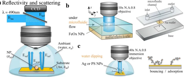
It is expected that such imaging relying on the change in light reflectivity of a sensing (reflecting) surface yields high sensitivity in terms of NP detection and imaging. Visualization of the NP light scattering in a reflection mode has several advantages compared to the most com-mon visualization operated in transmission mode (as usu-ally performed under classical dark-field illumination). As illustrated in Fig. 1a, when a NP is immobilized on a reflecting surface, here an Au-coated Si wafer, the light reflected by the surface may constructively interfere
Fig. 1 a Principle of reflectivity imaging of scattering NPs at a
gold-reflecting surface. b, c Schematic experimental configurations used for the monitoring (b) of 300 nm FeOx maghemite NPs
convection-adsorption in a microfluidic cell or c of the bouncing or irreversible adsorption of 40 and 60 nm Ag, or 100 nm PS NPs on a surface
with the light back-scattered by the illuminated NP. Such reflection imaging microscopies exploit interferometric [19–30] detection principles. They yield enhanced NP visualization with sensitivities, which have outperformed dark-field observations in some configurations named iSCAT [21–23], SP-IRIS [24–26], BALM [28–30], for, respectively, interferometric SCATtering microscopy, Single Particle Interferometric Reflectance Imaging Sensor, or Backside Absorbing Layer Microscopy. These methods have unprecedented sensitivities allowing the detection of down to 10 nm individual NP. Among them, the BALM technique is the only one exploiting such detection over a conductive surface (an ultrathin Au layer), which can be of interest for single-NP electro-chemical studies [28–30].
The present work shows that the simple reflectivity of a semi-infinite Au surface offers interesting performances for in situ single-NP visualization. For this purpose, we first establish an optical modeling of the operating princi-ple. This extends the model proposed from the similar SP-IRIS technique [24–26], however, adapted to the water-Au interface. It is exemplified for various NPs: absorbing iron oxide maghemite, FeOx, NPs, dielectric ones from polystyrene, PS, then metallic ones, such as Ag NPs. The model predicts that reflectivity imaging is particularly sensitive to the visualization of dielectric NPs with pre-dicted detection limit for PS or Ag NPs down to 30 nm, competing with current dark-field imaging techniques.
We then confirm experimentally this potentiality by monitoring the adsorption from colloidal solution of 300 nm FeOx NPs, 100 nm PS or 40 and 60 nm Ag NPs on a reflecting Au surface. This is performed under two experimental conditions presented in Fig. 1. The first example (Fig. 1b) shows how the technique can be employed to monitor the capture of individual magnetic FeOx nanobeads by a biosensor in a microfluidic environ-ment [31]. The second example (PS and Ag NPs, Fig. 1c) is more relevant to the electrochemical nanoimpact strate-gies used to detect, characterize and count individual NPs [32–34]. A question often considered in this emerging electroanalytical field concerns the dynamics of the NP motion associated to its electrochemical actuation at a detecting electrode. Herein, we propose to address this issue in the absence of electrochemical transformation, by optically monitoring the interaction of Ag or PS NPs at a non-polarized Au surface. More specifically, we present the influence of electrolyte on the ability of NPs to repeti-tively bounce or irreversibly adsorb onto the Au surface. Although not performed in an electrochemical environ-ment, the results will be of interest in comprehending and developing useful physical insight into single-NP electro-chemical studies.
2 Experimental
The detection of individual NPs freely moving in solution or adsorbed on an Au-coated Si wafer (Aldrich) was investigated in real time by light reflectivity microscopy. It was performed, as previously described [16–18], with an in-house devel-oped setup consisting of a standard microscope (Olympus) equipped with a water-immersion objective (Olympus LUMP-LFLN 40XW, 40 ×, NA 0.8), and a CCD camera (Photon-Focus MV-D1024E-160-CL). A light halogen source, filtered at 490 nm with an interference filter (spectral bandwidth of 20 nm), was used to illuminate, from the top solution and via the objective, the Au substrate. The reflected light, collected from the same objective, was sent to the CCD camera. Before experiments, the illumination incidence on the substrate sur-face to be imaged was adjusted with an accuracy of 0.01°, in the absence of solution, using an interference Mirau objective (Nikon, CF Di 20 × NA 0.4) by minimizing interference pat-terns. The colloidal solutions, prepared from commercial NPs solutions (FeOx from Ademtech®, PS NPs from Aldrich®, Ag
NPs from NanoComposix®) were then poured into the
home-made cell for in situ observation. The images of the reflecting surface on the CCD camera were captured through a home-programmed Labview software. Each image is a stack of five snapshots, each integrated over 50 ms. Each image is then taken every 1.86 s. Image analysis was achieved using Matlab routines.
3 Results and Discussion
3.1 Theoretical Background
3.1.1 Principle of the Reflectivity Measurement
Consider an electromagnetic planar wave, characterized by an incident electric field Einc, propagating in an ambient medium
A (of refractive index nA) towards a reflecting substrate M (of complex refractive index ̃nM = nM + i kM). Upon reflection, the
reflected planar wave is characterized by an electric field Eref
whose properties are given by Fresnel laws. Particularly, the signal I(x,y) recorded at each pixel location, x, y, at a detector (a CCD camera) corresponds to the modulus of the reflected field, |Eref(x,y)|2. For normal incidence, the reflectance, R,
which characterizes the amount of light reflected by the sur-face, is given from the Fresnel equation by,
In its simplest form, the incident light flux is not evalu-ated, and only the reflected light is collected on a CCD. Rel-ative reflectance measurements are obtained by comparing
(1) R= ||Eref|| 2 | |Einc|| 2 = | | | | nA− ̃nM nA+ ̃nM | | | | 2 .
successive images or times, t, as long as the incident illu-mination is kept constant. Comparing the signal recorded at each pixel I(x,y,t) to that recorded on the first image I(x,y,t = 0) allows monitoring of the local relative variation in reflectivity, ∆R(x,y,t)/R, from,
Under the λ = 490 nm blue light illumination used herein, an ideal reflecting Au substrate ( ̃nM. = 1.1 + 1.83i) immersed
in water (nA = 1.33) is expected to reflect toward the CCD camera 37% of the incident light, and our setup was shown to detect local variation of reflectivity down to ∆R/R = 0.002 [16–18], meaning variation in collected signal down to 0.2%.
3.1.2 Nanoparticle Detection by Reflectance Imaging Microscopy
One prospect of the enhancement of small NP visualization (Fig. 1a) is due to the fact that the field scattered by the NP is a spherical wave while the incident (or reflected) field is a plane wave. The signal I(x,y) recorded at each pixel cor-responds to the interference pattern of the back-scattered far-field Escat and a reference field, here the reflected field,
Eref, and I(x,y) writes:
where ϕ is the phase lag between both fields. While for a NP of diameter dNP the scattering signal ||Escat(x, y)||
2
usually scales as d6
NP, for small NPs the preponderant signal arises
from the interference term (last term in Eq. 4) and scales as the scattered field amplitude ||Escat(x, y)|| and, therefore, as d3
NP. It thus enables the detection of much smaller
nanoo-bjects than under dark-field illumination, enabling the real time and operando inspection of NP with sensitivity similar to standard scanning electron microscope [28].
The quantitative simulation of such interferometric far-field NP visualization has been proposed by Ünlü’s group [24–26]. They modeled by boundary element methods, BEM, the SP-IRIS configuration where a NP is immobilized on a flat multilayer substrate, made of a thin SiO2 dielectric
layer onto a reflective Si semi-infinite substrate. The NP is imaged from the top, in a reflection mode in an air medium. This configuration applies straightforwardly to the present case, more pertinent for electroanalytical applications, where a NP immobilized onto a flat Au substrate is imaged, from a top solution, through a water-immersion objective.
The adapted optical model, precisely described in Ref. [24–26], briefly consists of simulating the steady-state (2) I(x, y, t) I(x, y, t = 0) = R(x, y, t) R(x, y, t = 0) = 1 + ΔR(x, y, t) R(x, y, t = 0). (3) I(x, y) = ||Eref(x, y) + Escat(x, y)||
2
,
(4)
= ||Eref(x, y)|| 2
+ ||Escat(x, y)|| 2
+ ||Eref(x, y)||||Escat(x, y)|| cos(𝜙),
optical scattering of NPs on a reflecting substrate, by solving Maxwell’s equations via discrete numerical methods. BEM is preferred as it considerably speeds up the calculation pro-cess because it only requires the meshing of the different NP-medium interfaces (and not the whole volume as in finite element methods such as COMSOL®). Moreover, a Matlab
toolbox dedicated to the simulation of the scattered fields of nanoparticles on layered media is available online through the Magnetic Nanoparticle Boundary Element Method (MNPBEM) implementation [35–39]. It is implemented for a wide range of examples and codes for the SP-IRIS situa-tion that are also available online [38]. Modification of the latter codes to account for our experimental configuration is straightforward. Mostly, the ambient medium is changed from air to water (nA = 1.33), the substrate is changed from
layered SiO2/Si to Au (with refractive index obtained from literature [40]).
Typically, the geometry of the system is first defined: a monochromatic (λ = 490 nm) incident plane wave Einc
illuminates at normal incidence a NP of various materials (Ag, PS, Fe3O4; refractive indexes, ñNP, are, respectively, ̃
nAg = 0.135 + 2.71i, nPS = 1.61 and ̃nFe
3O4 = 2.36 + 0.07i, based on literature data [40]) immobilized on a semi-infinite Au substrate. In a first approach, the illumination was con-sidered as a single plane wave. A more rigorous approach would consider the decomposition of the illumination source into different incoherent plane wave components with dif-ferent incident angles. The overall image would then corre-spond to the superposition of the response of each of these individual components [24].
In the simpler approach proposed here, the far-field image collected on the detector is obtained from the interference of the normal incidence reflected plane wave (Eref) with the corresponding induced scattered field. The reflected field is obtained from the Fresnel formalism, as in Eq. (1). The MNPBEM toolbox is used to compute the far-field scattering Escat propagating along the whole microscope objective’s (NA = 0.8) collection solid angle. Finally, the image at the detector I(x,y) is obtained from Eq. (3) by coherently add-ing both reflected and scattered contributions at each pixel position (x, y) of the image plane.
3.1.3 Simulated Images of Nanoparticles by Reflectance Imaging Microscopy
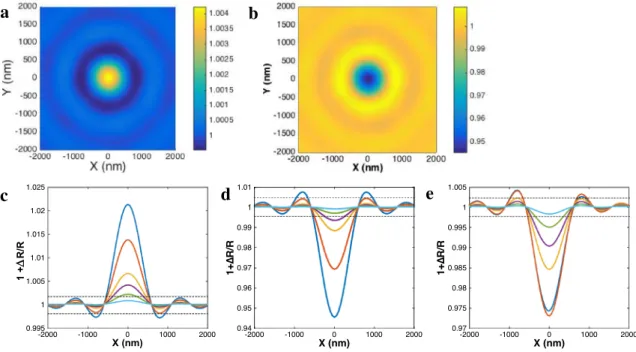
As detailed in Ünlü’s work, the images of NPs by reflectance microscopy depend on the properties of the NP material versus that of the reflecting substrate, but also on the NP to substrate distance and on the defocus of the observation. Figure 2 presents the simulated optical responses of NP materials chosen here. The simulated reflectivity images of a 40 nm metallic Ag NP and a 100 nm dielectric PS NP are given, respectively, in Fig. 2a, b, while the reflectivity
profile line of all materials (including the absorbing dielec-tric FeOx NP) for dNP ranging from 30 to 100 nm are
pre-sented in Fig. 2c–e. Over the Au-reflecting substrate, both PS and FeOx NPs are detected as negative contrast features, while the metallic NP appears as a bright contrast one. Actu-ally, the detection and the contrast of NPs depend on the refractive index of the NP material with respect to that of the substrate. For example, the presence of Au NP would be undetected on the Au substrate. Similarly, by changing the Au-reflecting substrate to the SiO2-coated Si substrate
employed in the SP-IRIS configuration, the NP contrasts become inverted: in SP-IRIS a metallic Ag NP (respectively, a dielectric PS NP) would appear as a negative (respectively, positive) feature.
In the case of the Au-reflecting substrate, illumina-tion at λ = 490 nm allows the highest contrast, since it is the spectral region where Au is the least refractive (high-est signal-to-noise ratio). Typically, the detection limit of ΔR/R > 0.002 suggests that 25 nm Ag NPs can be imaged individually at λ = 490 nm, while 100 nm Ag NPs would not be detected (ΔR/R = 0.0007) on an Au substrate illuminated at λ = 633 nm.
3.2 Experimental Illustrations of Reflectance Imaging Microscopy of Nanoparticles on Au Substrates
This section presents the ability of reflectance microscopy for analytical and electroanalytical case studies devoted to
the imaging of the interaction of NPs with Au surfaces. Two experimental examples are presented, which display the monitoring of the individual NP behavior in colloidal solutions above an Au surface. Although no electrochemical actuation is performed here, the examples show the collision of individual NPs with surfaces. Such collisions are encoun-tered in different analytical and electroanalytical situations. Irreversible adsorption of a target NP is generally sought in the design of nanobead-based microfluidic biosensors. The first explored example employs 300 nm magnetic maghemite nanobeads flowing through a microfluidic channel. NP col-lision and interaction with metallic surface are usually stud-ied in the electrochemical nanoimpact strategy. The second example is illustrated here with either dielectric 100 nm PS NPs or 40 and 60 nm metallic Ag NPs.
3.2.1 Sensing Single Nanobead Attachment on an Au Sensor in a Microfluidic Environment
Commercial 300 nm carboxy-functionalized maghemite NPs were dissolved into a milli-Q water solution at a concentra-tion of 108 NPs/mL. This solution was injected into a
micro-fluidic channel constructed from an Ibidi sticky-slide® of
5 × 0.8 mm2 section mounted atop an Au-coated Si substrate.
The Au surface is used as the NP sensing or the recognition platform. The dimension of the sensor in contact with the solution of NPs is 5 × 10 mm2 and only a 1 × 1 mm2 surface
at the stream front is imaged, as shown in Fig. 3a. To permit the capture of the NPs, the Au surface, corresponding to
a
b
c
d
e
Fig. 2 Simulated reflectance images of a a 40 nm Ag and b 100 nm
PS NPs located at the center of the image. Reflected intensity line profile along the y or x axis as a function of the NP size for c Ag,
d PS and e Fe3O4 NPs of diameter 20, 30, 40, 50, 75 and 100 nm;
dashed lines correspond to the ± 0.002 limit of detection for the reflectance measurement
the bottom surface of the channel, is functionalized by dip-coating with a thin layer of polyethyleneimine (ca. < 10 nm). This modified surface is denoted Au/PEI. At the natural pH of the milli-Q water, the Au/PEI presents a positive charge facing the flowing aqueous colloidal solution. This enables electrostatic interaction with the negatively charged NPs, and, therefore, the capture of the NPs. The sensor surface reflectivity is then monitored while circulating the colloidal solution at a low magnification, with a 10 × objective micro-scope. Images of the light reflected by the Au/PEI surface are taken from the top through the Ibidi slide cover and the colloidal solution. This allows probing the largest possible
regions of the sensor, typically 1 mm2, which for example
can evidence capture dynamics heterogeneities, but is at the detriment of the image resolution (1px is ca. 1 µm2).
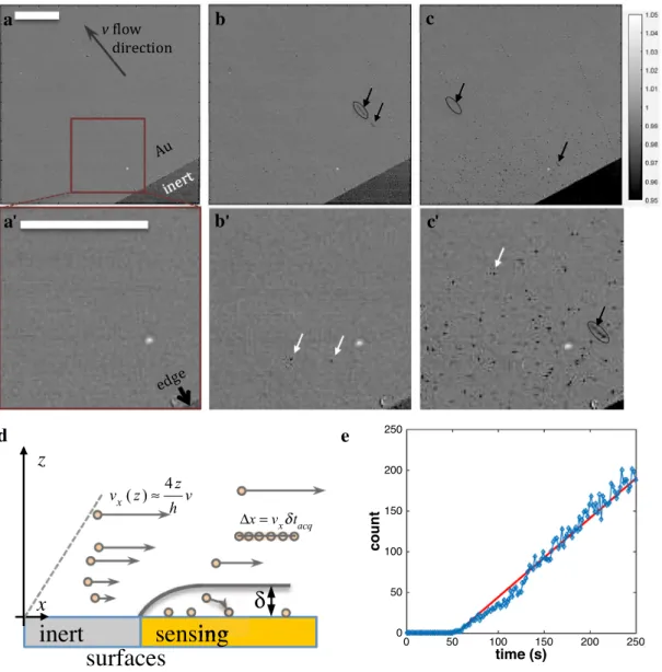
Figure 3a–c shows selected snapshots of the Au/PEI surface taken (a) while a pure water solution was flow-ing (absence of NP) in the channel with a fluid velocity of 4 mm/s (flow rate 1 mL/min), then (b, c), respectively, 5.4 and 72 s after the detection of the first adsorption events resulting from the flow of the colloidal NP solution.
Different features can be identified on these images (zoom in Fig. 3a’–c’). Dark spots appearing on the sur-face correspond to individual adsorbed NPs (examples
a
d
e
a
b
b
c
c
Fig. 3 Images of the bottom surface of a microfluidic channel dur-ing the flow of solution a before and b, c after injection of 300 nm maghemite colloidal solution. b and c are taken, respectively, 5.4 and 72 s after the first NP adsorption event is detected (5.4 s after
a). a’–c’ Zoomed selections from a–c. Bar = 200 µm. Arrows on the
images show some examples of flowing (black arrows) or adsorbed (non-moving, white arrows) NPs. d Scheme describing the convective
layer of thickness δ from which NPs are captured and how to estimate NP altitude from the length ∆x of linear segments (image acquisition
δtacq = 300 ms) and the local velocity expression (assuming z ≪ h and with v the fow velocity expressed at mid-channel height z = h/2). e Evolution of the number of adsorbed NP counted (blue symbols) over the images in a–c and compared to Eq. 6 (red line)
pointed by white arrows in Fig. 3b’, c’). They can be dif-ferentiated from NPs moving downstream, identified as the linear segment trajectories caught during the 300-ms camera exposure. Although they are not in the focal plane of the observation, the camera can catch these moving NPs to the point of estimating their individual velocity, vx.
The examples circled in Fig. 3b, c yield NPs with veloci-ties vx = 250 and 950 µm/s. From such particle trajectory tracking, one is then able, as schematized in Fig. 3d, to estimate the altitude of the NP or, as discussed elsewhere, to probe, with a resolution dictated by the NP dimension, the fluid flow dynamics [41]. Here, assuming the NPs are submitted to a parabolic Poiseuille flow profile, one can infer the moving NPs altitude from the Au substrate and along the h = 800 µm channel height. The example veloci-ties suggest that the NPs are localized between 12.5 and 48 µm from the sensor surface. Interestingly the visualiza-tion from the top and through the soluvisualiza-tion allows visual-izing and detecting NPs present in solution, even though they are out of focus.
These images also suggest, as proposed by the optical model, that FeOx NPs can readily be detected by reflectiv-ity measurements. However, the low magnification cannot strictly be compared to the model as each NP is detected as an individual (1 pixel) spot of negative contrast (lesser reflectivity than the original Au/PEI substrate). In average, the different spots correspond to a ca. 2.2 ± 0.4% loss of reflectivity (1 + ΔR/R < 0.978 ± 0.004), which compares the reflectivity change predicted for 100 nm FeOx NPs in Fig. 2e (1 + ΔR/R = 0.975).
Such optical monitoring also provides further information in NP-based sensing applications [42–44]. The number of NPs captured by the sensor, for example within the selected zoomed region, can be counted over time through the dark spot detection on each image. It allows inspecting the NP capture dynamics. For efficient adsorption events (with prob-ability close to 1), the capture is mass transfer limited and the NP capture frequency is expected to reflect the NP mass transfer properties. Here, large flow rates over large sensor length along the flow direction, l = 1 cm, compared to the channel height, h = 0.8 mm, are used. Under these condi-tions, the only target NPs that can be captured by the sensor are coming from a thin depletion layer adjacent to the sensor, as schematized in Fig. 3d. The thickness of this depletion layer, δ, within the microfluidic convective regime scales as the inverse of the third root of the flow rate, v; the higher the flow rate is, the thinner the δ:
The frequency of NP capture per cm2 of sensor surface
area, fsurf, then relies on the flux of NPs reaching the sensor
surface by diffusion within this diffusion layer δ. Newman (5)
𝛿∼ 1
v1∕3.
[45] computed this situation, which may also be computed from Comsol® [46]. For large velocities, one obtains:
with DNP and CNP, the NP diffusion coefficient and
concen-tration in the colloidal solution, respectively. For the 108 NP/
mL colloidal solution of 300 nm NPs of DNP= 1.6 µm2/s, the
NP captured is then expected to increase linearly with time, with a slope equal to fsurf. Figure 3e shows that the
experi-mental number of NPs capture indeed follows such linear trend with a slope of 9.5 × 10² NP/cm2/s, in good agreement
with the value of the mass transfer-limited flux density of 9 × 10² NP/cm2/s obtained from (6). This particularly
sug-gests that such imaging configuration allows not only prob-ing the NPs concentration in the solution from their capture frequency, but also differentiating NPs freely moving in solution (out of focus) from adsorbed ones.
3.2.2 Visualizing Single Sub‑100 nm Nanoparticle Immobilization on a Sensing Au Surface
Adsorption of NPs is also an important issue in the elec-trochemistry of individual NPs. Different authors [47–50] demonstrated that when large dielectric insulating spheres (from 150 nm to µm) collide with an UME, they irrevers-ibly adsorb onto it. This adsorption sufficiently blocks the mass transfer of a redox probe toward the UME so that each individual adsorption event can be monitored elec-trochemically from a step-like transient (decrease) in UME current. Fodsick et al. later confirmed this hypothesis from the simultaneous optical and electrochemical visualization of the irreversible adsorption of fluorescent-labelled micro-spheres [50].
The dynamics of PS NPs collision with an Au surface was imaged through a water-immersion objective (40 ×, NA 0.8) immersed directly in a colloidal solution of PS NPs, as schematized in Fig. 1c. Figure 4a presents 100 × 75 µm2
ROIs of reflectivity images of the Au surface (separated by 350-s interval) after it was contacted with 5 mL of milli-Q water colloidal solution of 100 nm PS NPs. Clearly these images show diffraction-limited dark, less reflecting, fea-tures appearing on the Au surface over time (see arrows in zoomed 25 × 25 µm2 ROIs in Fig. 4a’).
The evolution of the reflected light variation along lines crossing two examples of NPs were extracted from images and compared in Fig. 4b to the predicted profiles. If the profile widths are consistent with diffraction-limited imaged nanoobjects, the reflectivity variations, ∆R/R, cor-responding to the different NPs detected are within − 0.7 and − 1.4%, which based on the proposed model suggests the detection of NPs with equivalent size between 40 and (6) fsurf= 0.81DNPCNP ( v DNPlh )1∕3 ,
50 nm. This discrepancy is owing to the relative nature of the measurement and rather suggests that the Au substrate is more reflective than predicted: it would result in a higher background reflectance and of a lower relative reflectance change for the NPs.
The adsorption dynamic of individual NPs was also monitored. As shown in Fig. 4c for the variations of local reflectivity at selected point positions on the images, the adsorption of single NPs is instantaneous at the experimental acquisition rate (≤ 300 ms). Finally, the superlocalization of the centroid of the PS NPs along time suggests that the NPs are strongly bound to the Au surface and do not notice-ably move during tens of seconds. The same conclusions are drawn for other NPs that keep adsorbing as time goes. In agreement with earlier reports for larger dielectric polymeric spheres, the collision of the PS NPs leads to irreversible adsorption events.
Metallic or electrochemically active NPs can also be detected from a current (or potential) transient recorded while they collide onto a polarized electrode. A variety of nanomaterials have been probed from such electrochemical nanoimpact strategy. From the variety of current-transient features or from the frequency of collision events, differ-ent NP-electrode collision scenarii were proposed: from irreversible adsorption to repetitive bouncing (or electrode-surface detachment) of NPs. The latter multiple-bites col-lision of a same NP on an electrode is easily inferred for
the collision of catalytic Pt NPs [32]. The same conclusion was also inferred in the case of the irreversible transforma-tion of NPs upon their collision to the UME, such as the oxidative electrodissolution of Ag NPs. The sub-ms resolu-tion of single-NP current transients shows multiple time-separated current spikes related to the multistep incomplete electrochemical dissolution of Ag NPs [51]. This was con-firmed from Monte Carlo or multiphysic modeling of the NP Brownian motion during the electrochemical nanoimpact process suggesting indeed the possible escape of NPs after a short and incomplete charge transfer [52–54]. In principle, these situations may be differentiated optically. The optical monitoring, in 3D [11–14] by holography or in 2D by SPR [7, 8, 55, 56], of the reaction did not show such significant NP escape but rather that the NP stays close by (< 300 nm) to the electrode surface until its complete dissolution. On one hand, these experiments then suggest that if NPs are partially dissolved, allowing their desorption, they may not be evacuated in the solution, at least with the Brownian dynamics of a freely diffusing NP. On the other hand, the probability of NP escape from the electrode can be increased when the electrochemical cell dimension is reduced [57]. Indeed, by confining the NP into the end of a nanopipette, the probability of NP ejection from the electrode, imaged by fluorescence microscopy, increases as a result of the increas-ing importance of the electrostatic repulsion of the NP by the nanopipette walls. Although this points to the importance of
a
a
b
c
Fig. 4 Au surface reflectivity imaging of the adsorption of 100 nm PS NPs from a milli-Q water solution. a Examples of a 100 × 75 µm2
ROI of reflectivity images taken 350 s apart, with zoom of the red ROI in a’. b Reflectivity change profile along selected lines;
experi-mental data (points) compared to model profiles (lines) for, respec-tively, 40, 50, 60 and 100 nm. c Examples of the dynamics of selected single NPs adsorption events through the recording of local reflectiv-ity variation at selected pixel positions over time
electrostatic effects when decreasing the electrochemical cell volume, it may differ from the situation encountered in most electrochemical nanoimpacts studies.
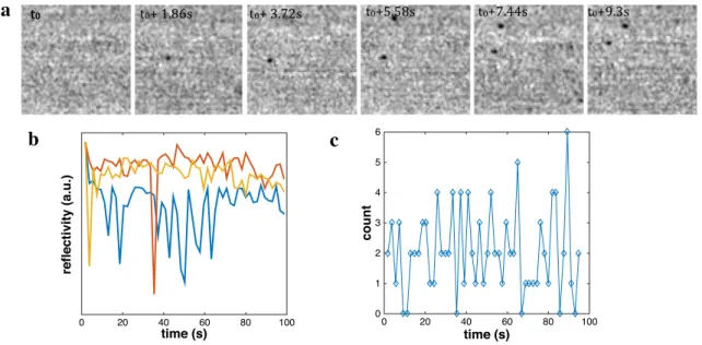
To advocate for such phenomena, we have monitored the collision of individual Ag NPs with a Au surface in the absence of applied electrochemical potential, therefore, avoiding the complicated NPs dissolution leading to their optical disappearance. The dynamics of Ag NPs collision at a non-polarized Au surface was imaged through a water-immersion objective (40 × , NA 0.8) immersed directly in the colloidal solution, as schematized in Fig. 1c.
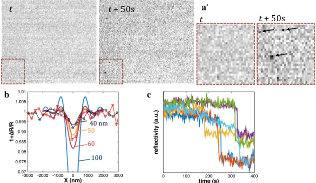
The reflectivity of an Au surface in contact with a solution, made of 10µL of a 0.02 mg/mL 60 nm Ag NPs diluted in 5 mL milli-Q water (final Ag NP concentration CNP = 3.5 × 10⁷ NP/mL) was imaged. Figure 5a presents
suc-cessive frames of a selected 50 × 50 µm2 ROI of the Au
sur-face. As for FeOx and PS NPs, diffraction-limited dark fea-tures considered as NPs are observed on these frames. At the observation frequency, these features are now moving over successive frames and no irreversible adsorption of the NPs could be monitored. This is confirmed from Fig. 5b, which presents the average local reflectivity variation measured over even smaller ROI (1 × 1 µm2 or 10 × 10 µm2). Indeed,
single or multiple individual reflectivity spikes are detected over the entire movie. These reflectivity spikes differ from the steps recorded for PS NPs and show that single or, at best, 2 NPs appear and disappear stochastically from these small ROIs. Similarly, Fig. 5c presents the counting of dark features appearing over time over a larger 125 × 100 µm2
ROI of the Au substrate. Individual NPs also occasionally appear in this ROI, but the amount of NPs does not increase as is expected for irreversible adsorption processes (for FeOx NPs, see Fig. 3e). These observations suggest that Ag NPs do not adsorb irreversibly on the Au surface and are rather exploring, by Brownian motion, large areas of the Au surface.
The maximum steady-state mass transfer-limited flux density of NPs per surface area reaching the ROI of sur-face area S = 1.3 × 10⁻⁴ cm2 can be approximated (For
a disk of radius a UME the flux of diffusing NP is given by 4DNPCNPa with S = πa2 yielding to a flux density f = 4
DNPCNP/π1/2S1/2 = 2.25 D
NPCNP/S1/2. For a square UME of
side length l [12], the flux is given by π/21/2 D
NPCNPl and
S = l2 yielding to a flux density f = 2.22 D
NPCNP/S1/2) by
fsurf≈ 2.2DNPCNP/S1/2 with D
NP = 8.3 µm2/s for 60 nm NPs.
A density frequency of 5.6 × 10² NP/cm2/s, or equivalently
a frequency of 0.07 NP/s would then be expected over the 100 × 125 µm2 ROI. This suggests that over the ca. 100 s,
one would be able to detect ca. 7 NPs, which is in agreement with the average number of NPs, ca. 2, constantly detected in Fig. 5c. Meanwhile, the successive frames in Fig. 5a suggest that the same NPs are counted several times even though not on the same position of the ROI. This agrees with the features of constrained Brownian motion generally observed when Brownian nanoobjects trajectories are analyzed close to walls. It also agrees with the multi-bites nanoimpacts or bouncing NPs postulated earlier [51–54]. These multiple bouncing collisions can be detected optically here with Ag
a
b
c
Fig. 5 Reflectivity monitoring of 60 nm bouncing Ag NPs in
milli-Q water (< 20 µM citrate) solution. a A same 50 × 50 µm2 region of
interest (ROI) is presented over successive frames (acquisition time 50 ms) taken every 1.8 s: two dark features, considered as NPs, are changing location between frames; b stochastic reflectivity spikes
detected from local reflectivity averaged over 1 × 1 µm2 (yellow and
orange traces) or 10 × 10 µm2 (blue trace) ROIs; c number of NPs
counted over a 125 × 100 µm2 ROI: the number of NPs detected
NPs since the NPs are not subjected to any electrochemical transformation (dissolution).
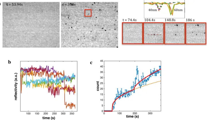
The bouncing of Ag NPs may seem at odds with ear-lier correlated optical observation of their dissolutive elec-trochemical nanoimpacts [7, 11, 55]. It is likely due to the repulsive interaction between the stabilized citrate-capped NPs and the Au surface. Indeed, their behavior is drastically altered when electrolyte is present in the solution. This can be performed, either by adding a 1 mL 20 mM NaCl solu-tion to the 5 mL Ag NP milli-Q solusolu-tion or by injecting aliquots of stock Ag NP solutions to a 10 mM NaCl solution. Figure 6 illustrates such experiment in which a first 5µL ali-quot of 40 nm Ag NPs (final CNP= 6 107 NP/mL) is injected
into a 5 mL NaCl 10 mM solution at t = 48 s, followed by the injection of a second 10µL aliquot of 60 nm Ag NPs (final CNP= 3.5 107 NP/mL) at t = 200 s. Figure 6a shows
the images taken after injection and at the end of the experi-ment of a 100 × 75 µm2 ROI showing the coverage of the Au
surface by multiple dark features. A series of zoomed images of a 10 × 10 µm2 ROI of the Au surface recorded during
this experiment are also displayed for t = 74.4, 100.4, 148.8, 186 s, showing that these dark features are now fixed over the same location, suggesting their irreversible adsorption.
Some optical intensity profile lines of selected dark features also suggests that they correspond to diffraction-limited objects, supposedly NPs. From these profiles, it also seems that the optical reflectivity decreases for larger NP sizes. These observations, as those made in the absence of NaCl, suggest that Ag NPs can be detected by simple microscopic observation in a reflection mode, even though the loss of reflectivity is at odds with the optical prediction (gain in reflectivity) presented above.
Selected examples of the time evolution of the local reflectivity variation estimated over different 1 µm2 ROIs
are presented in Fig. 6b. This contrasts totally from the stochastic NP bouncing detected in the absence of NaCl. Indeed, reflectivity steps are now detected, suggesting the irreversible adsorption of the NPs in the presence of NaCl.
The same conclusion is drawn from the evolution of the number of dark features counted over the 100 × 75 µm2 ROI
of the Au surface (Fig. 6c). Apart from a short time interval following each injection, where optical perturbations may lead to an artificial increase in NP surface population, the number of NPs steadily increases over the time. The flux of NPs reaching the Au surface is fed by NP linear diffusion from the solution while the Au surface continuously removes
a
b
c
Fig. 6 Reflectivity imaging of 40 and 60 nm Ag NPs irreversible adsorption onto a reflecting Au surface upon injection of aliquots of 40 (at t = 53 s) and 60 nm (at t = 200 s) of NP solutions into a 5 mL 10 mM NaCl solution. a Examples of reflectivity images of a 100 × 75 µm2 ROI of the Au surface with zoomed 10 × 10 µm2 ROI at
t = 74.4, 100.4, 148.8, 186 s and examples of reflectivity profile lines
of selected 40 (left) and 60 (right) nm Ag NPs. b Examples of reflec-tivity transients showing the irreversible NPs adsorption. c Evolution of the number of NPs counted over the 100 × 75 µm2 ROI in a
them from the solution. This is conceptually analogous to the dissolutive electrochemical nanoimpact experiments, except that the NPs here are not dissolved, only irreversibly adsorbed, at the Au surface. One can then estimate this flux from the knowledge of the NP content in solution, CNP. It is anticipated that the NP mass transfer or frequency, f, is given by linear diffusion profile [43], following Cottrell’s law, then:
from which the number of NPs reaching the Au surface, nNP(t), is obtained by integration:
The two solid lines in Fig. 6c present the predicted vari-ations from Eq. (8) for, respectively, the 40 nm (faster dif-fusing and more concentrated) and 60 nm NPs. The sum of these curves reproduces nicely the experimental varia-tions. The fit of the experimental variations is obtained with CNP40= 4.5 × 10⁷ NP/mL and C
NP60= 3.4 × 10⁷ NP/mL, which
compares well with the respective expected values of 6 and 3.5 × 10⁷ NP/mL.
It then suggests that the increasing number of dark fea-tures adsorbing on the Au surface are nanoobjects present at the same concentration and moving analogously with the injected Ag NPs. We attribute these dark features to indi-vidual Ag NPs. It cannot be excluded that for the 40 nm NPs dimers or agglomerates are preferentially detected.
This demonstration of irreversible and quantitative (mass transfer limited) adsorption of Ag NPs on surfaces when they are in electrolytic solution (at least > 10 mM here) suggests that care should be taken when performing or interpreting electrochemical nanoimpacts. It is frequently assumed that NPs remain stable in electrolytic solutions. But dissolved salts can have many effects on the NPs and their local environment as modifying the pH, increasing the ionic strength, desorbing the NP capping agent, etc. The consequences on the NP behavior also depend on the NP size, the NP shape, the capping agents, or the chosen elec-trolyte. The NP stability is, therefore, difficult to predict and has to be investigated for new experimental conditions prior to nanoimpacts experiments upon the possibility of making mistakes in evaluating the NP size dispersion based on spike charges and/or the NP concentration based on the impact frequency. This is one of the reasons why nanoimpacts are more and more coupled to a second complementary analysis technique. The effect of electrolytic solution on NP aggrega-tion was for example demonstrated from soluaggrega-tion phase NP tracking [58, 59]. Here, we use the reflectance microscopy (7) f = SC√NPDNP 𝜋DNPt, (8) nNP(t) = 2CNPS √ DNPt 𝜋 .
to highlight the importance of surface adsorption effects. The introduction of NaCl, even at the 10 mM level seems to strongly affect the NP environment and its interaction with a surface, even in the absence of electrochemical polariza-tion. By destabilizing the colloidal solution, the NPs tend to adsorb irreversibly on surfaces. This study shows that reflectance microscopy is an elegant way for further study in situ the effect of the chemical and physical (such as size, charge, or polarizability) nature of the ions of an electrolyte to destabilize colloidal NPs. For polymeric or biologic nano-materials or nanoparticles coated by such constituents, the nature of each ionic component of an electrolyte is indeed known to alter (chaotropic effect) or promote (kosmotropic effect) hydrogen bonds networks yielding in, respectively, the destabilization or stabilization of their colloidal solu-tions. Similar studies could be envisioned under optical monitoring or electrochemical actuation.
From the electrochemical nanoimpact prospect, it sug-gests that even if multiple bytes current transients have been previously detected electrochemically [51–53], the adsorp-tion strength is stronger than the suggested escape of the NP into the solution, at least over distances larger than > 300 nm.
Another possible reason should then be invoked to explain the multiple dissolutive bites observed electrochemi-cally. The presence of oxide or pseudo-halide shell layer, or even its formation during the oxidative process, in the pres-ence of residual halide ions, even at the sub-mM level, could impair the NP-electrode contact resistance and the overall electrodissolution process. The role of such oxide layer on Ag NP dissolution was recently demonstrated from single-NP optical birefringence visualization [60, 61].
Moreover, the irreversible adsorption of NPs will appar-ently decrease the NP solution content especially in high surface-to-volume cell configurations: such as small volume pipetting or high dilution processes, or maybe in nanoelec-trochemical cell. Similarly, the adsorption of NPs to the UME insulating walls [62] may also be a strong competing source of NP depletion, which can be taken into account by readjusting the frequency-CNP relationship. It may for
example explain the often observed decrease of NP impact frequency over long acquisition times (as predicted by the establishment of a pseudo-linear diffusion regime expected over cylindrical UMEs [34]).
Finally, Ag NPs are experimentally detected as dark fea-tures, which is at odds with the optical prediction. If some bright feature may be detected, the majority of features (> 95%) are darker. Such discrepancies can account for the selection of incorrect values of the Au substrate and/or solu-tion and/or Ag NP refractive indexes in the model. Slight alterations of the Au and solution indexes could indeed change the amount of reflected light. However, pure Ag NPs should still appear as bright features. One possibility could rather be that Ag NPs are covered by a thin layer of
oxide [60] (or AgCl) formed by their spontaneous oxidation in an O2-saturated NaCl solution. It is difficult to evaluate
precisely the effect of such a layer; however, from mean field approximation theories (such as Maxwell–Garnett) a 2 nm coating of AgCl over a 40 nm core Ag NP may yield a strong enough change in the apparent refractive index of the NP and explain the dark feature on an Au surface.
4 Conclusion
Dielectric and metallic NPs can be visualized at the single-NP level by simple imaging of the light reflected by a reflect-ing surface. An optical BEM modelreflect-ing, extendreflect-ing Ünlü’s work, predict that both dielectric PS and metallic NPs can be individually visualized, without any label, by collecting the local reflectance change of an Au surface. The model shows that such reflectivity imaging provides an interferometric detection, allowing one to enhance the optical detection sensitivity. If 30 nm NPs should be theoretically detected, it is anticipated that other reflecting substrates could be used similarly without needing dark-field illumination conditions. The further advantage of this interferometric detection is that dielectric NPs can also be detected, as negative contrast (dark or less reflecting) features, which is a considerable advantage compared to microscopies relying on dark-field illumination.
A microscope operating in the reflection mode was used to image, through solution, or even microfluidic cover, the dynamics of NP capture on an Au-sensing surface. First, starting with large 300 nm FeOx magnetic nanobeads in a microfluidic environment, it is shown how such NPs are optically detected, at the single-NP level, and counted. The strategy can be used to analyze the convective adsorption of NPs onto a large sensing area. This may be of interest for monitoring in real time and in situ the dynamics of nanoenti-ties capture in microfluidic biosensors.
It can also be used to monitor electrochemical processes occurring at single NPs. Even if no electrochemical activa-tion was used in this work, the Au surface monitored opti-cally could also be polarized in an electrochemical configu-ration. The present work shows that individual 100 nm PS NPs as well as 40 and 60 nm Ag NPs can be imaged through a water-immersion objective directly immersed between a colloidal solution and the Au surface, from their ability to alter the local reflectivity of an Au surface. If PS NPs appear as dark features, in agreement with the predicted model, Ag NPs are detected similarly, although they should be detected as bright features. This is attributed to the likely presence of Ag oxide or halide layer. The dynamic monitoring of the NPs behavior over the Au surface shows that PS NPs strongly and irreversibly adsorb to Au. The same observa-tion is made for Ag NPs when prepared in an electrolytic
solution (10 mM NaCl), while in the absence of electrolyte, the multiple bouncing of the NPs is evidenced. This con-firms previous simultaneous opto-electrochemical studies, which were at odds with multiple bouncing suggested from high time resolution electrochemical nanoimpacts. Ag NPs, in the absence of polarization, stand for tens of seconds on the Au surface, without showing Brownian exploration of the solution after they have contacted the electrode. We pro-pose that the presence or formation of poorly conducting Ag oxide or halide may also explain the multiple electrochemi-cal bites behavior.
As a perspective of this work, reflectance microscopy is a simple yet powerful tool that has allowed monitoring electrochemical processes [15–18, 63]. It does not require a transparent electrode unlike methods relying on dark-field illuminations, it is not restricted to Au electrodes, but to many reflecting surfaces [18], and can be performed at standard glass-insulated microelectrodes [16], or be coupled to local probing such as STM [63]. Based on these reported results, we expect that the technique could be applied to imaging the electrochemical reactivity of a wide range of NPs at the single entity level.
Acknowledgements We are grateful for financial support by the Agence Nationale pour la Recherche (NEOCASTIP ANR-15-CE09-0015-02 project) and Direction Générale de l’Armement (AMMIB ANR-13-ASTR-0021-01), by Universities Paris Diderot and Paris Sud and by CNRS.
References
1. Bard AJ, Mirkin MV, editors. Scanning electrochemical micros-copy. 2nd ed. Boca Raton: CRC Press; 2012.
2. Bentley CL, Kang M, Unwin PR. Scanning electrochemical cell microscopy: new perspectives on electrode processes in action. Curr Opin Electrochem. 2017;6:23–30.
3. Shan XN, Patel U, Wang SP, Iglesias R, Tao NJ. Imaging local electrochemical current via surface plasmon resonance. Science. 2010;327:1363–6.
4. Shan XN, Diez-Perez I, Wang LJ, Wiktor P, Gu Y, Zhang LH, Wang W, Lu J, Wang SP, Gong QH, Li JH, Tao NJ. Imaging the electrocatalytic activity of single nanoparticles. Nat Nanotech. 2012;7:668–72.
5. Fang YM, Wang W, Wo X, Luo YS, Yin SW, Wang YX, Shan XN, Tao NJ. Plasmonic imaging of electrochemical oxidation of single nanoparticles. J Am Chem Soc. 2014;136:12584–7.
6. Yuan T, Wang W. Studying the electrochemistry of single nano-particles with surface plasmon resonance microscopy. Curr Opin Electrochem. 2017;1:17–22.
7. Nizamov S, Kasian O, Mirsky VM. Individual detection and electrochemically assisted identification of adsorbed nanoparti-cles by using surface plasmon microscopy. Angew Chem Int Ed. 2016;55:7247–51.
8. Nizamov S, Scherbahn V, Mirsky VM. Detection and quantifica-tion of single engineered nanoparticles in complex samples using template matching in wide-field surface plasmon microscopy. Anal Chem. 2016;88:10206–14.
9. Peng Y, Xiong B, Peng L, Li H, He Y, Yeung ES. Recent advances in optical imaging with anisotropic plasmonic nano-particles. Anal Chem. 2015;87:200–15.
10. Jing C, Reichert J. Nanoscale electrochemistry in the “dark-field”. Curr Opin Electrochem. 2017;6:10–6.
11. Brasiliense V, Berto P, Combellas C, Tessier G, Kanoufi F. Electrochemistry of single nanodomains revealed by three-dimensional holographic microscopy. Acc Chem Res. 2016;49:2049–57.
12. Brasiliense V, Patel AN, Martinez-Marrades A, Shi J, Chen Y, Combellas C, Tessier G, Kanoufi F. Correlated electrochemical and optical detection reveals the chemical reactivity of individual silver nanoparticles. J. Am Chem Soc. 2016;138:3478–83. 13. Patel AN, Martinez-Marrades A, Brasiliense V, Koshelev D,
Bes-bes M, Kuszelewicz R, Combellas C, Tessier G, Kanoufi F. Deci-phering the elementary steps of transport-reaction processes at individual Ag nanoparticles by 3D superlocalization microscopy. Nano Lett. 2015;15:6454–63.
14. Batchelor-McAuley C, Martinez-Marrades A, Tschulik K, Patel AN, Combellas C, Kanoufi F, Tessier G, Compton RG. Simultane-ous electrochemical and 3D optical imaging of silver nanoparticle oxidation. Chem Phys Lett. 2014;597:20–5.
15. Munteanu S, Garraud N, Roger JP, Amiot F, Shi J, Chen Y, Com-bellas C, Kanoufi F. In situ, real time monitoring of surface trans-formation: ellipsometric microscopy imaging of electrografting at microstructured gold surfaces. Anal Chem. 2013;85:1965–71. 16. Munteanu S, Roger JP, Fedala Y, Amiot F, Combellas C, Tessier
G, Kanoufi F. Mapping fluxes of radicals from the combination of electrochemical activation and optical microscopy. Faraday Discuss. 2013;164:241–58.
17. Fedala Y, Munteanu S, Kanoufi F, Tessier G, Roger JP, Wu C, Amiot F. Calibration procedures for quantitative multiple wave-lengths reflectance microscopy. Rev Sci Instrum. 2016;87:013702. 18. Chakri S, Patel AN, Frateur I, Kanoufi F, Sutter EM, Mai Tran
TT, Tribollet B, Vivier V. Imaging of a thin oxide film formation from the combination of surface reflectivity and electrochemical methods. Anal Chem. 2017;89:5303–10.
19. van Dijk MA, Lippitz M, Orrit M. Far-field optical microscopy of single metal nanoparticles. Acc Chem Res. 2005;38:594–601. 20. van Dijk MA, Lippitz M, Stolwijk D, Orrit M. A common-path
interferometer for time-resolved and shot-noise-limited detection of single nanoparticles. Opt Express. 2007;15:2273–87. 21. Lindfors K, Kalkbrenner T, Stoller P, Sandoghdar V. Detection
and spectroscopy of gold nanoparticles using supercontinuum white light confocal microscopy. Phys Rev Lett. 2004;93:037401. 22. Kukura P, Ewers H, Müller C, Renn A, Helenius A, Sandoghdar
V. High-speed nanoscopic tracking of the position and orientation of a single virus. Nat. Methods. 2009;6:923–7.
23. Ortega-Arroyo J, Kukura P. Interferometric scattering micros-copy (iSCAT): new frontiers in ultrafast and ultrasensitive optical microscopy. Phys Chem Chem Phys. 2012;14:15625–36. 24. Sevenler D, Avci O, Ünlü MS. Quantitative interferometric
reflec-tance imaging for the detection and measurement of biological nanoparticles. Biomed Opt Express. 2017;8:2976–89.
25. Avci O, Adato R, Ozkumur AY, Ünlü MS. Physical modeling of interference enhanced imaging and characterization of single nanoparticles. Opt Express. 2016;24:6094–114.
26. Avci O, Ünlü NL, Ozkumur AY, Ünlü MS. Interferometric reflec-tance imaging sensor (iris) - a platform technology for multiplexed diagnostics and digital detection. Sensors. 2015;15:17649–65. 27. Boccara M, Fedala Y, Bryan CV, Bailly-Bechet M, Bowler C,
Boccara C. Full-field interferometry for counting and differentiat-ing aquatic biotic nanoparticles: from laboratory to Tara Oceans. Biomed. Opt Express. 2016;7:3736–46.
28. Lemineur J-F, Noël J-M, Ausserré D, Combellas C, Kanoufi F. Combining electrodeposition and optical microscopy for probing
size-dependent single-nanoparticle electrochemistry. Angew Chem Int Ed. 2018;57:11998–2002.
29. Lemineur J-F, Noël J-M, Combellas C, Ausserré D, Kanoufi F. The promise of antireflective gold electrodes for optically moni-toring the electrodeposition of single silver nanoparticles. Faraday Discuss. 2018;210:381–95.
30. Stockmann TJ, Lemineur J-F, Liu H, Cometto C, Robert M, Com-bellas C, Kanoufi F. Single LiBH4 nanocrystal stochastic impacts
at a micro water vertical bar ionic liquid interface. Electrochim Acta. 2019;299:222–30.
31. Squires TM, Messinger RJ, Manalis SR. Making it stick: con-vection, reaction and diffusion in surface-based biosensors. Nat Biotech. 2008;26:417–26.
32. Xiao X, Bard AJ. Observing single nanoparticle collisions at an ultramicroelectrode by electrocatalytic amplification. J. Am Chem Soc. 2007;129:9610–2.
33. Zhou YG, Rees NV, Compton RG. The electrochemical detection and characterization of silver nanoparticles in aqueous solution. Angew Chem Int Ed. 2011;50:4219–21.
34. Sokolov SV, Eloul S, Kätelhön E, Batchelor-McAuley C, Compton RG. Electrode-particle impacts: a users guide. Phys Chem Chem Phys. 2017;19:28–43.
35. Garcia de Abajo FJ, Howie A. Retarded field calculation of electron energy loss in inhomogeneous dielectrics. Phys Rev B. 2002;65:115418.
36. Hohenester U, Trügler A. MNPBEM – A Matlab toolbox for the simulation of plasmonic nanoparticles. Comput Phys Commun. 2012;183:370–81.
37. Waxenegger J, Hohenester U, Trügler A. Plasmonics simulations with the MNPBEM toolbox: consideration of substrates and layer structures. Comput Phys Commun. 2015;193:138–50.
38. MNPBEM toolbox. 2018. http://physi k.uni-graz.at/mnpbe m/. Accessed 20 Dec 2018.
39. Codes developed for the SP-IRIS. 2018. https ://githu b.com/derin seven ler/SP-IRIS-BEM. Accessed 20 Dec 2018.
40. Refractive index values are tabulated. 2018. https ://refra ctive index .info/. Accessed 20 Dec 2018.
41. Brasiliense V, Berto P, Aubertin P, Maisonhaute E, Combellas C, Tessier G, Courty A, Kanoufi F. Light driven design of dynamical thermosensitive plasmonic superstructures: a bottom-up approach using silver supercrystals. ACS Nano. 2018;12:10833–42. 42. Wang W, Tao NJ. Detection, counting, and imaging of single
nanoparticles. Anal Chem. 2014;86:2–14.
43. Wo X, Li Z, Jiang Y, Li M, Su Y-W, Wang W, Tao NJ. Determin-ing the absolute concentration of nanoparticles without calibration factor by visualizing the dynamic processes of interfacial adsorp-tion. Anal Chem. 2016;88:2380–5.
44. Kuzmichev A, Skolnik J, Zybin A, Hergenröder R. Absolute anal-ysis of nanoparticle suspension with surface plasmon microscopy. Anal Chem. 2018;90:10732–7.
45. Newman J. The fundamental principles of current distribution and mass transport in electrochemical cells. In: Bard AJ, editor. Electroanalytical chemistry, vol. 6. New York: Dekker; 1973. p. 279–97.
46. Fuchs A, Fermigier M, Combellas C, Kanoufi F. Scanning electro-chemical microscopy. Hydrodynamics generated by the motion of a scanning tip and its consequences on the tip current. Anal Chem. 2005;77:7966–75.
47. Quinn BM, van’t Ho PG, Lemay SG. Time-resolved electro-chemical detection of discrete adsorption events. J Am Chem Soc. 2004;126:8360–1.
48. Boika A, Thorgaard SN, Bard AJ. Monitoring the electrophoretic migration and adsorption of single insulating nanoparticles at ultramicroelectrodes. J Phys Chem B. 2013;117:4371–80. 49. Suraniti E, Kanoufi F, Gosse C, Zhao X, Dimova R, Pouligny
manipulated by optical tweezers in the vicinity of ultramicroelec-trodes. Anal Chem. 2013;85:8902–9.
50. Fosdick SE, Anderson MJ, Nettleton EG, Crooks RM. Correlated electrochemical and optical tracking of discrete collision events. J Am Chem Soc. 2013;135:5994–7.
51. Oja SM, Robinson DA, Vitti NJ, Edwards MA, Liu Y, White HS, Zhang B. Observation of multipeak collision behavior during the electro-oxidation of single Ag nanoparticles. J Am Chem Soc. 2017;139:708–18.
52. Ma W, Ma H, Chen JF, Peng Y-Y, Yang Z-Y, Wang H-F, Ying Y-L, Tian H, Long Y-T. Tracking motion trajectories of individ-ual nanoparticles using time-resolved current traces. Chem Sci. 2017;8:1854–61.
53. Ustarroz J, Kang M, Bullions E, Unwin PR. Impact and oxidation of single silver nanoparticles at electrode surfaces: one shot versus multiple events. Chem Sci. 2017;8:1841–53.
54. Robinson DA, Liu Y, Edwards MA, Vitti NJ, Oja SM, Zhang B, White HS. Collision dynamics during the electrooxidation of indi-vidual silver nanoparticles. J Am Chem Soc. 2017;139:16923–31. 55. Sun L, Fang Y, Li Z, Wang W, Chen H-Y. Simultaneous optical
and electrochemical recording of single nanoparticle electrochem-istry. Nano Res. 2017;10:1740–8.
56. Sun L, Wang W, Chen H-Y. Dynamic nanoparticle-substrate con-tacts regulate multi-peak behavior of single silver nanoparticle collisions. ChemElectroChem. 2018;5:2995–9.
57. Hao R, Fan Y, Zhang B. Imaging dynamic collision and oxidation of single silver nanoparticles at the electrode/solution interface. J Am Chem Soc. 2017;139:12274–82.
58. Robinson DA, Kondajji AM, Castañeda AD, Dasari R, Crooks RM, Stevenson KJ. Addressing colloidal stability for unambigu-ous electroanalysis of single nanoparticle impacts. J Phys Chem Lett. 2016;7:2512–7.
59. Sokolov SV, Tschulik K, Batchelor-McAuley C, Jurkschat K, Compton RG. Reversible or not? Distinguishing agglomeration and aggregation at the nanoscale. Anal Chem. 2015;87:10033–9. 60. Sundaresan V, Monaghan JW, Willets KA. Visualizing the effect of partial oxide formation on single silver nanoparticle electrodis-solution. J Phys Chem C. 2018;122:3138–45.
61. Smith JG, Jain PK. The ligand shell as an energy barrier in sur-face reactions on transition metal nanoparticles. J Am Chem Soc. 2016;138:6765–73.
62. Eloul S, Compton RG. Shielding of a microdisc electrode surrounded by an adsorbing surface. ChemElectroChem. 2014;1:917–24.
63. Di N, Damian A, Maroun F, Allongue P. Influence of potential on the electrodeposition of co on Au(111) by in situ stm and reflectiv-ity measurements. J Electrochem Soc. 2016;163:D3062–8.