DESIGN OF A CRYOTRON COMPUTER
by
FRED HERZFELD
JUN
171iU
L
E
R AR'
SUBMITTED IN PARTIAL FULFILLMENT OF THE REQUIREMENTS FOR THE DEGREE OF
BACHELOR OF SCIENCE
at the
MASSACHUSETTS INSTITUTE OF TECHNOLOGY
Signature of
Certified by
June, 1958
Signature Redacted
Author ... . .. ..Department of Electric Engine e ring, May 26, 1958
Signature Redacted
. . . .
...
....
..
..-
.
.
.
.
.
.
.
.
.
.
.
.
.
..
Signature Redacted
Accepted by
. . .
. . . .
C.. .. . . . . .. . . . .Chai an, Departmental Committee of Theses
-i-DESIGN OF A CRYOTRON COMPUTER by
FRED HERZFELD
Submitted to the Department of Electrical Engineering on May 26, 1958 in partial fulfillment of the requirements for the degree of Bachelor of Science.
ABSTRACT
The work reported in this thesis is the development of the logical and associated circuitry of a general purpose digital computer employing cryotrons.
Following a discussion of the basic switching functions in two forms of realizations, and a discussion of a pulse detector with complementary output, the general organization of the cryotron computer is presented.
Diagrams of the computer logical circuitry and the asso-ciated terminal equipment are given. A read-out amplifier for the low-level cryotron output was designed, constructed, and tested in a cryotron circuit. Proper operation of the read-out amplifiers in conjunction with cryotron circuits was achieved. A method of building the cryotron computer in plug-in modules is presented. Coupling between modules is mag-netic.
ACKNOWLEDGMENT
I wish to express my deepest appreciation to Dr. Dudley A. Buck for suggesting the topic of this thesis, for the patient guidance and supervision of the work, and for editing and criticising the completed thesis.
I alsowish to thank Mr. Arthur J. Schneider, Mr. Kenneth R. Shoulders, and Mr. Merle L. Wetherell for the many helpful discussions,
and Allan F. Pacela for his aid in the con-struction.
I am indebted to Professor Ewan W. Fletcher for providing the laboratory facilities, and to the Lincoln Laboratory Division 6 Document Room for reproducing the thesis.
-111-TABLE OF CONTENTS
page Abstract
Acknowledgment
Table of Contents iii
List of Illustrations
CHAPTER I INTRODUCTION
1. 1 History 1
1.2 Objective 2
CHAPTER II BASIC CRYOTRON SWITCHING CIRCUITS
2.1 The Single Cryotron 3
2. 2 The Basic Circuits
2. 21 Circuits and Notation 3
2.22 The OR Circuit 4
2.23 The AND Circuit 6
2.24 The NOT Circuit 6
2.25 The INHIBIT Circuit 6
2.26 The Flip-Flop 8
2.27 The DELAY 8
2.28 The Pulse Detector 8
CHAPTER III GENERAL ORGANIZATION
3.1 Specifications 13
3.2 Pulse Sequence 18
3. 21 The Instruction Cycle 18
3.22 The Execution Cycle 20
CHAPTER IV THE COMPUTER CIRCUIT
4. 1 The Memory Unit
4.11 The Memory 26
4. 12 Memory Selection Matrix 28
4. 2 The Print Unit
4.21 The Print Register 28
4. 22 The Ten Position Switch 28
4.23 The Print Translation Matrix 32
4. 24 Flexowriter Routine Circuit 32
4. 3 High Speed Fast Access Counter 35
4.4 The Accumulator Unit
4.41 The A Register 38
-iv-4.43 The B Register 41
4.44 The Adder 41
4.5 The Bus Register 41
4. 6 The Instruction Counter 43
4.7 The Control 43
4.8 The Instruction Selection Matrix 43
4.9 The Clock 45
4.10 The Clock Gates 45
4. 11 The Overflow Register 48
4. 12 Product Sign Digit Register 48 4. 13 Command Line Selection Matrices
4. 13-1 Addition 51
4.13-2 Subtraction 51
4. 13-3 Multiplication 54
4.13-4 Clear and Add 54
4. 13-5 Store 54 4. 13-6 Transfer 58 4. 13-7 Transfer if Negative 58 4.713-8 Transfer on Overflow 58 4. 13-9 Shift Right 58 4. 13-10 Shift Left 62 4.13-11 Print 62
4.14 The Read-In Unit 65
CHAPTER V TERMINAL EQUIPMENT
5. 1 Output 71
5.2 Input 75
CHAPTER VI CONSTRUCTION OF CRYOTRON CIRCUITS
6. 1 Superconductive Joints 76
6.2 Modular Construction 76
CHAPTER VII CONCLUSIONS
7. 1 Summary 78
7. 2 Suggestions for Further Research 79
APPENDIX I COMMAND LINES 80
LIST OF ILLUSTRATIONS Figure Number 1 2
3
4
5
6
7 89
10 11 12 13 14 1516
17 18 19 20 21 22 23 24 25 26 Title General OR Circuit General AND Circuit Inhibit GateCryotron Flip.Flop Circuit Cryotron Delay Circuit Complementation Circuit Computer Panel
Block Diagram of Cryotron Computer Cryotron Flip-Flop Memory
Memory Selection Matrix Tree Print Register
Ten position switch for Print Translation Matrix Print Translation Matrix
Flexowriter Print Routine Circuit High Speed Fast-Access Counter Single Order Cryotron A Register
Adder with End-Around-Carry Network Instruction Selection Matrix
Cryotron Clock The Clock Gates
The Overflow Storage and checking Register Product Sign Digit Register
Command Line Selection Matrix for Addition Command Line Selection Matrix for Subtraction Command Line Selection Matrix for Multiplication Command Line Selection Matrix for Clear and Add
Page
5
S7
9
10
12 17 19 27 2930
31 33 34 37 39 42 44 46 47 49 50 52 5355
56
-vi-LIST OF ILLUSTRATIONS
(c ontinue d)
Title
Command Line Selection Matrix for Storage Command Line Selection Matrix for Transfer Command Line Selection Matrix for Transfer if Negative
Command Line Selection Matrix for Transfer on Overflow
Command Line Selection Matrix for Shift Right Command Line Selecti6n Matrix for Print Flexowriter Translation Matrix 1
Flexowriter Translation Matrix 2 Number-Symbol Selection Matrix Code Matrix
Read-out Amplifier
Read-out Amplifiers and Plug Board
Page Figure Number 27 28 29 30 31 32 33 34 35 36 37 38 57
59
60
61
6364
66
67 6869
72 74-1-CHAPTER I
INTRODUCTION 1. 1 HISTORY
In the evolution of science and technology the trend toward more complex systems has forced a continual search for means to minia-turize, to investigate and apply the various phenomena of solid-state devices.
In the computer field there has been the ever more important search for methods which will increase the speed of operation of the computer. There are three solutions to the combined problem of attaining small size and high speed. First, new circuitry which will permit the present relatively slow components to function more efficiently, as for example, an otherwise slow counter employing high speed carry propagation. Second, the development of new
com-ponents which are inherently applicable as high speed devices. Along with these two solutions there is the possibility of reduction in size through smaller construction and packaging. The third and perhaps most important region in which we hope to find solutions to the problem is in a combination of new circuitry with new components which are not only fast but small. This then is the problem: Find
a new component which is inherently small and develop the associated new circuitry. In this thesis we will be dealing mainly with the
circuitry of a newly developed component.
The development of the cryotron I by D. A. Buck has opened another path along which we may hope to achieve both high speed and microminiaturization. The cryotron consists of a
-2-conductor whose superconductive state may be destroyed by the appli-cation of a magnetic field. It is a two-state device operating in the temperature region near absolute zero; dissipating power only during
the transition period; easily fabricated in extremely small s .ze; and whose upper switching frequency limit has been estimated betweer
100 and 1, 000 megacycles.
Operation at this low temperature implies not only that the device has a very low noise level, but also that it will have an ex-tremely long life. Its two-state nature implies simple circuitry for a binary system. Dissipation of power during the switching transition only means less formidable requirements on the power source. The
small size in which the cryotron may be fabricated means that larger systems can be packaged into a smaller space. . Along with these advantages there is the possibility of extreme speed as the cryotron becomes physically smaller.
1.2 OBJECTIVE
There are four parts that will be considered. First, the design of a small general purpose stored program digital computer using cryotron circuitry. Second, the design of reliable read-out amplifiers. Third, the construction of both the computer and the associated terminal equipment. Last and most important, the testing of the computer to determine the reliability of the cryotron in a large system. We will proceed from the discussion of the
capabilities of the cryotron itself to the analysis of the Block Diagram logic, through the circuitry of the individual blocks and the problems of construction.
-3-CHAPTER I
BASIC CRYOTRON SWITCHING CIRCUITS
2. 1 THE SINGLE CRYOTRON
The basic component of the computer, the cryotron, is a device which depends on the destruction of superconductivity by a magnetic
2
field. The behavior of the cryotron is somewhat like an electro-3
mechanical relay, and yet between them there is a distinct difference in the number of "contacts" and in "contact resistance". A single electromechanical relay can have any number of contacts or contact pairs, while a single cryotron can have only normally closed contacts, and in the usual wire-wound form of construction has only one normally closed (superconductive) contact. The resistance of the open contact on an electromechanical relay is essentially infinite, preventing current flow. The cryotron gate (contact), on the other hand,
presents approximately 0. 001 ohm when resistive, thus as a series type switch it introduces only a small resistance which has little or no effect on the current flow. The closed contacts of the electro-mechanical relay present only a very small resistance, while the gate resistance of the superconductive cryotron is exactly zero. Useful switching with the cryotron can be accomplished by intro-ducing the very small gate resistance into a path in which is flowing, and at the same time providing an alternate superconductive path for the current; that is, using it as a parallel switch.
2. 2 THE BASIC CIRCUITS
2.21 CIRCUITS AND NOTATION
In the design of digital computers there are a number of basic circuits from which any functional relationship may be synthesized. In particular there are the OR, AND, NOT, and INHIBIT circuits.
-4-The FLIP-FLOP and the DELAY are also of great importance as
individual circuits although they may be constructed through the use of the simpler basic circuits. A PULSE DETECTOR of importance
when the input signal is not in complementary form had to be developed.
Throughout the discussion we will make use of the TRANSMTSSTON
rather than the HINDRANCE notation, and the duality that exists between the two systems will be particularly noted in a comparison
of the OR and the AND circuits.
2.22 THE OR CIRCUIT
The two general equations which specify the OR circuit may be
written as:
K
F: ZAk EA ' k (la, b)
where the A ks and the A k's are the complementary inputs. F and F
represent the complementary outputs. While it is usual to consider only Equation la for the OR function, it was stated that an alternate shunt path for the current must be provided, and this is given in equation form by the dual of Equation la, namely lb. The realization
of these switching functions in terms of cryotron hardware is shown in Figure 1. This is only a typical circuit, and it must be recognized that many other circuit realizations of the functions ( la, b) are
possible. For the condition F= 0 we note that the source current
I must flow through the control of cryotron C The gate of C must therefore be resistive, and that of C superconductive. For any other input condition we have F= 1 and there are one or more gates on the F side which will be resistive, and one or more gates on the F side which will be superconductive. The source current I must
5
therefore flow through the control of cryotron C . The outputs may be determined by sensing the gates of C and C2'
A
AK A2 A2
is AK
C C
F F
FIGURE I GENERAL OR CIRCUIT
Is AK A2 A A2 is A CI C 2 F F
GENERAL AND CIRCUIT
-6-2.23 THE AND CIRCUIT
We have previously mentioned the hindrance and transmission notations of Boolean Algebra as applied to switching circuits, the two systems being mathematical duals. Thus we may notice that the general equations for the AND circuit given by Equations 2a, b are the duals of Equations la, b.
F=T Ak F Ak (2a, b)
Except for an exchange in variables, 2a, b and la, b are identical and all that is required is an exchange of input lines and an exchange of output interpretation. This is shown in Figure 2. This duality is of particular importance in cryotron circuitry since the shunt or dual path must be present, and complementary inputs and outputs are also
usually necessary.
2.24 THE NOT CIRCUIT
The NOT circuit performs an inversion of the input variable. Thus for cryotron circuitry, since both the variable and its comple-ment are usually present, the NOT circuit may be realized by an interchange of the output lines. If however the input is not present in complementary form the reader is refered to section 2. 28 where a method of obtaining the complement is given.
2.25 THE INHIBIT CIRCUIT
The INHIBIT function may be stated as:
F= X&Y Fa X+Y (3a, b)
where Y is the inhibitor and X and Y any variables or function of variables. Figure 3 is a simple form of this function as realized without the use of dual X inputs although complementary Y inputs are
required, and is a GATING TYPE realization. The INHIBIT circuit may also be realized by a proper choice of inputs to the AND circuit.
Y -INPUT
xi
00 0 OUTPUT o X INPUT 0 Y INPUT INHIBIT GATE FIGURE 3-8-2.26 THE FLIP-FLOP
A simple form for the FLIP-FLOP was shown to be that given in Figure 4a, with the block symbol representing it shown in Figure 4b. If we consider the source current I flowing through the gate of C , the gate of C2 being resistive, then it must also flow through the g'ate
of C3 and through the controls of C and C In flowing through the control of C it will prevent itself from flowing through the gate of C2. The inputs are no longer required and the source current will
remain in the same path. If an input is now applied to the control of C1 , the current will decay in the first path and build up in the
alter-nate one and the FLIP-FLOP WILL change its state, which may be sensed by testing the output gates of cryotrons C5 and C For such switching to occur the magnitude of the current Is is given by Equation 4, and further details on the switching may be found in reference 4.
I (I
(I
(4)
c s C
where Ic is the magnitude of the current at the threshold of switching.
2. 27 THE DELAY
A digital time delay may be achieved by interconnecting a series of FLIP-FLOPS in such a manner that a pulse travels down the line, flipping one after the other, as shown in Figure 5. Input and output gates may be combined thus requiring only four cryotrons per delay time plus two output cryotrons. By using only four cryotrons it is also possible to get short unit delay times.
2.28 COMPLEMENTARY-OUTPUT PULSE DETECTOR It is pointed out above that the cryotron lends itself best to complementary circuitry. There are however times when compple-mentary inputs are not readily available, as for example in pulse detection, and it is necessary to use a circuit which will convert the presence or absence of a pulse into complementary outputs, one
ONE INPUT 0 ZERO OUTPUT
Is FLIP- FLOP
ZERO INPUT ONE OUTPUT
ONE INPUT
CR I
CR 3
CR5
ZElto OUTPUTZERO INPUT
CR 2
CR
4CR 6 ONE
OU TPUT(A") (a)
(A) CRYOTRON FLIPFLOP CIRCUIT (8) BLOCK SYMBOL
DELAYED
PULSE INPUT OUTPUT PULSE
C - FF F F FF FF
COMPLEMENT
I s OUTPUT
FIGURE 5 CRYOTRON DELAY CIRCUIT
-11-indicating that a signal is present and the other -11-indicating that there
is no signal. The circuit diagram of such a pulse detector is shown
in Figure-6.
When there is no input pulse, cryotrons C and C3 have no current flowing in their control windings. The gates of C and C3 are therefore superconductive. The source current Is has only one path available through which it may flow, namely through the control of C2 and the gate of C . This is the only superconducting
path since there is a resistance in series with the other, produced
by the gate of C2 through the control of which the source current
must always flow. This method of producing the resistance is used in order that the magnitude of the resistance is approximately that of any normal gate; however any resistance of proper magnitude may be substituted. Thus the current must choose the path which is
entirely superconductive.
If there is a pulse present, C and C3 have -current flowing in their control windings. The gates of C and C3 are therefore resistive. The source current Is now has two parallel resistive
paths in which to flow, and the current in the control of C is deter-minedby the ratio of the two resistances. Assuming that the
resistances are equal, the current in the control of C will be less
4
than I , the transition current (the restriction on I is again given
c s
by Equation 4. ) and the gate of C will be superconductive, while the gate of C3 is resistive.
As shown in the diagram the source current Is may be applied to the gates of C3 and C to sense their state and the outputs thus
INPUT IN U NO INPUT CR3 C R I CR 2C4 YES INPUT 'Is
FIGURE 6 COMPLEMENTATION CIRCUiT
-13-CHAPTER III
GENERAL ORGANIZATION
3. 1 SPECIFICATIONS
The design of a computer must start with a decision as to what. the computer is to be capable of performing. Since the purpose of this thesis is to develop the logical and associated circuitry of a
general purpose digital computer using cryotrons for all of the switch-ing elements, it is of importance to decide which functions or commands will best illustrate the use of cryotrons in a large system and provide a means for evaluating the performance of the system. For this purpose we have chosen to design a single address machine which has the 14 instructions listed in Table 1. While these 14 are only
a few of the many instructions which could be built into the computer they will serve to illustrate the design principles. The number of digits in a word determines the precision with which the computer can handle numbers, and for the cryotron computer a word length of 11 binary digits was arbitrarily chosen. If one of these 11 is used for the sign digit (or the Tag for instructions) the number of digits for the address part of an instruction is fixed at 6 and the number of words in storage at 64. With 64 storage locations it will be possible to operate the computer with several program loops for long-time operation evaluation.
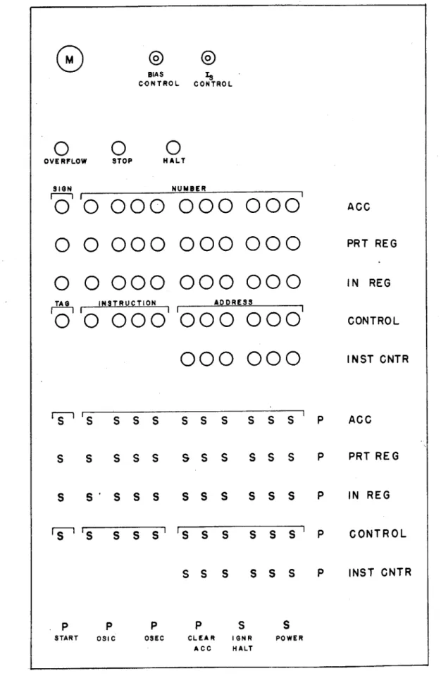
The computer panel was designed to provide as much flexibility as could reasonably be expected. The panel layout is shown in
Figure 7. It provides visual observation of the data in the
ACCUMULATOR, INPUT and OUTPUT registers, the INSTRUCTION COUNTER and the CONTROL register. For each of these there
is a set of switches, (S), provided for manually correcting or setting the data at any of the mentioned units at a computer HALT POINT, and a push button, (P), for transfering the information
-14-TABLE I
INSTRUCTION SYMBOL CODE DESCRIPTION
Stop STP 0000 Computer stops regardless
of information in acdress part of instructions.
In-dicates STOP on panel.
Add ADD 0001 The number stored at the
indicated address is added to the contents of the acc-umulator, and the sum re-mains in the accumulator.
Subtract SUB 0010 The number stored at the
indicated address is sub-tracted from the contents of the accumulator and the difference remains in the accumulator.
Multiply MUL 0011 The number stored at the
indicated address is mul-tiplied by the contents of the accumulator. The eleven least significant remain in the M register.
Clear and Add CLA 0100 The accumulator is
re-set to zero and the num-ber stored at the indicat-ed address is placindicat-ed in the accumulator.
F
-15-Store STRTRA
Transfer Transfer if Negative Transfer on Overflow Shift Right TRN TRO SHR0101
0110
0111 1000 1001The number in the acc-umulator is placed in the indicated storage loca-tion; previous content of the storage location is discarded, and the con-tents of the accumulator remain unchanged.
The next instruction is taken from the address
indicated.
The next instruction is taken from the address indicated if the sign of
the accumulator is neg-ative, otherwise the next instruction is taken in normal sequence. Zero is interpreted as negative.
The next instruction is taken from the address indicated if an overflow occured on the previous operation, other-wise the next instruction is taken in normal sequence. Overflow register reset; accumulator remains un-changed.
The number in the acc-umulator is shifted to the right by the number of places indicated in the address part of the instruc-tions. Sign remains un-changed. Shifted digits enter the M register.
F
-16-Shift Left Print SHL
PRT
Halt Point HLT Read In RDN 1010 1011 1100 1101The number in the acc-umulator is shifted to the left by the number of places indicated in the address part of the
in-structions. Digits shifted to the left of the tenth order are discarded. Sign remains unchanged.
The word at the indicated
address is placed in the PRINT register and
printed by the Flexowriter as a SIGN plus four octal
digits.
Computer comes to a halt.
All registers remain
un-changed. Computer will start with the next instruc-tion in sequence when ex-restarted. Indicates HALT on panel.
The number in the input register is placed in the memory at the location specified by the address part of the instructions. Previous contents of the memory location are discarded.
o
0
0
OVERFLOW STOP HALT
SIGN NUMBER
05I
0000
000
0 0000
000
000
000
0 0 000 000 000
TAG 0 INSTRUCTION ADDRESS
I
0lI
000"'000 000,
000 000
s ss
s s s
s s s
I
P ACC PRT REG IN REG CONTROL INST CNTR ACC S S S S S S S S S S S P PRT REG S s s S S Sj1 5 S S P P PSTART OSIC OSEC
SS S S S S P IN REG Is S S s s S P S CLEAR IGN ACC HAL s s s I P CONTROL S S S P INST CNTR S R POWER T
FIGURE 7 COMPUTER PANEL
,'S
BIAS IS
-18-stored in the switches to the respective register. Visual indication
is provided for the OVERFLOW, PROGRAM STOP and HALT POINT. Switches are provided for PROGRAM START, OPERATE SINGLE INSTRUCTION CYCLE, OPERATE SINGLE EXECUTION CYCLE, CLEAR ACCUMULATOR, CLEAR INSTRUCTION
REGISTER, and IGNORE HALT POINT.
A meter and two potentiometers are provided to monitor the
source current and properly set the level of the read-out amplifiers.
3.2 PULSE SEQUENCE
From the basic Block Diagram of the cryotron computer,
Figure 8, the sequence of pulses necessary for the various instructions was determined. To minimize the number of such pulses for a given instruction, the sequence was arranged so that a given pulse could
perform several functions simultaneously. The generation of the pulses and the switching networks which distribute them are discussed in detail in Chapter IV of this thesis; in this section the pulse sequences for each of the various instructions are determined. Each sequence is divided into two distinct cycles - the instruction cycle and the execution cycle.
3. 21 THE INSTRUCTION CYCLE
One of the pulses of every command either advances the instruc-tion counter by ONE or, if it is a transfer command, places the
transfer address in the instruction counter. The last pulse from any of the execution matrices routes the clock pulses to the
instruc-tion cycle selecinstruc-tion matrix. If the computer is being started manually the instruction counter is set to the address of the first instruction (usually zero) and the clock pulses are diverted from both- the
INSTRUCTION COUNTER
I
CONTROL INSTRUCTION I ADDRESS CLOCK PULSE COUNTER COMMAND LINE SELECTION MATRIX + + + + U+ + TO ALL UNITS A- REGISTER M-REGISTER ADD E R B-REGISTE M EMOR Y BUS REGISTER PRINT aRECONTROLBLOCK DIAGRAM OF CRYOTRON COMPUTER
INPUT REGISTER & CONTROL INSTRUCTION SELECTION MATRIX MEMORY SELECTION MATRIX
4
I
FIGURE 8 I r-20-button is depressed. The pulse sequence to the various command lines for performing the INSTRUCTION CYCLE is given in Table 2.
3.22 THE EXECUTION CYCLE
The pulse sequence during the operation of the EXECUTION CYCLE is also determined from the Block Diagram. Since one of the instructions allows a TRANSFER ON OVERFLOW, the first pulse in every sequence with the exception of the PRINT is a test for overflow. The pulse sequence for the various commands during the execution cycle is given in Table III. Having determined the
sequence of pulses that is required for the various arithmetic operations we turn to the design of the individual units.
TABLE II
PULSE NUMBER OPERATION
P0 Cut off command lines
P1 Read Memory into Bus
P2 Read Bus into Control
-21-TABLE III
PULSE NUMBER OPERATION
ADDITION P 0 P 1 P 2 P 3 P4
Cut off command lines Test for overflow
Read Memory into Bus
Read Bus into B register Read A register into Adder Read B register into Adder Pulse Carry to Add
Read sum into A register Advance Instruction counter Switch clock to instruction cycle
P5
P6
SUBTRACTION p 0 P P 2 P 3 P 4 P 5 P6Cut off command lines
Test for overflow Read Memory into Bus Read Bus into B register Read A register into Adder Read B register into Adder Pulse Carry to Add.
Read sum into A register Advance Instruction counter Switch clock to instruction cycle.
F
-22-Cut off command lines Test for overflow
Read A register into Bus Read Bus into Memory
Advance Instruction Counter Switch clock to instruction cycle
TRANSFER
Cut off command lines Test for overflow
Read Address into Instruction counter Switch clock to Instruction cycle
TRANSFER IF NEGATIVE
Cut off c ommand lines Test for overflow
Read address into Instruction counter if sign of A register is negative
Switch clock to Instruction cycle
TRANSFER ON OVERFLOW P P I P 2 STOP P0
Cut off command lines
Pusle TRANSFER ON OVERFLOW line
Switch clock to Instruction cycle
Pulse to STOP flip-flop of clock
STORE P ,0 P 1 P 2 P 3 P 4 P 0 P P2 P3 P 0 P P2 P 3
-23-MULTIPLY
P Cut off command lines
P Test for overflow
P2 Read Memory into Bus
P3 Read A register into B register via
complement if necessary
Read Bus into M register via complement
if necessary
Store sign in SIGN storage register
P ZERO set A register
4
ZERO set Adder
P5 Read A register into Adder
Read B register into Adder
Pulse carry to Add if right hand order of M register is ONE
P6 Read sum into A register if right hand order of M register is ONE
Py 7Shift Right
P8 Zero set sign order
The sequence of pulses P P 7 and P each occur a total
5'1 6'1 7 8
of ten times in the above sequential order
P45 Complement A register if necessary via
sign storage register
P46 Advance Instruction counter
P47 Switch clock to instruction cycle
HALT
P0 Pulse to Halt flip-flop of clock
READ IN
P0 Cut off command lines
P Test for overflow
-24-Read Bus into Memory Advance Instruction counter
Switch clock to instruction cycle
CLEAR AND ADD
P0 P P2 P3 P 4 P 5 SHIFT RIGHT P0 P 1 P2 P3 Pal P an P am
Cut off command lines Test for overflow Read Memory into Bus Read Bus into B register ZERO set A register
Read A register into Adder Read B register into Adder
Pulse carry to Add
Read sum into A register Advance Instruction counter Switch clock to instruction cycle
Cut off command lines Test for overflow
Read ADDRESS into counter Advance instruction counter First shift right pulse
Last shift right pulse
Switch clock to instruction cycle
SHIFT LEFT
Identical to SHIFT RIGHT except that Pal through Pan go to shift left command line
P 3
-25-PRINT
P
Cut off command lines
P
Read memory into Bus
P
Read Bus into Print register
ZERO set print counter
P
Advance instruction counter
P
4Pulse to print flip-flop
P
5Detour clock pulses from print command
-26-CHAPTER IV
COMPUTER CIRCUIT
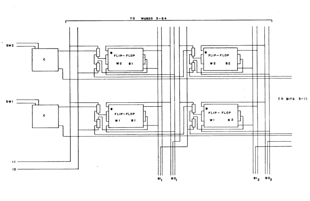
4.1 THE MEMORY UNIT 4. 11 THE MEMORY
The cryotron Flip-Flop memory of the computer was designed to read information into and out of the Bus register. Each bit in the memory consists of a flip-flop and two gating cryotrons as is shown in Figure
9.
The output gates of the same order in each word are connected in parallel and are labeled BI (Bus Input) as are the input controls of the same order in each word (labeled BO - Bus output).The two gating cryotrons for each bit determine whether that
particular bit will deliver a pulse to the Bus or receive a pulse from the Bus. The gating cryotrons of every bit in a word are all connect-ed in series and are driven by the complementation circuit, as shown, so that when there is no input to the complementation circuit these gates are cut off, or resistive. When a complementation circuit has an input applied, the gating cryotrons of this word are superconductive. Selection of a word, then, is accomplished by applying an input to the complementation circuit which represents the chosen word.
Reading to and from the Bus is now accomplished by a pulse to either command line 11 or 12.
The current on either of the command lines (11 or 12) can flow only through the bit selection gates of the selected word thus preventing other words from responding.
The source current for the complementation circuits is not shown in Figure 9. However, all the source currents in the computer are in series, and therefore only one external current source is
TO WORDS 3-64 SW2 C SW I l2 12 FLIP- FLOP W2 SI FLIP-FLOP WI SI FLIP- FLOP W2 82 FLIP - FLOP WI e 2 I - - - - i 1 8il Bo I TO BITS 3-Il '2 BO2
FIGURE 9 CRYOTRON FLIP-FLOP MEMORY WITH COMMAND LINES TO BUS REGISTER
-28-4.12 THE MEMORY SELECTION MATRIX
The MEMORY SELECTION MATRIX is realized in the form
of a tree rather than a rectangle in order to reduce the number of cryotrons in any series path, and therefore to reduce the time constant of the circuit. The circuit is shown in Figure 10. The outputs of the six digits of the ADDRESS part of an instruction
enter at the top of the Figure, and a source current Is enters the tree and is distributed through the gates as shown. The output lines, labeled 0 through 63, go to the respective word selection
complementation circuit inputs denoted SWxx in Figure 9.
4.2 THE PRINT UNIT
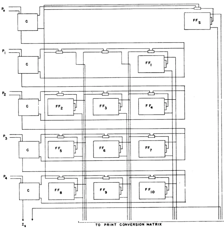
4. 21 THE PRINT REGISTER
The PRINT REGISTER operates along the same lines as the memory, requiring only one gating cryotron per bit. The register
is always being read out into the PRINT TRANSLATION MATRIX, by the current Is and the information is changed by properly
applying pulses to the complementation circuits. Flip-Flop FF stores the sign of the word to be read out. FF stores the most significant digit, and all other FF's are grouped in threes as an
octal code. The four output lines go to the TEN POSITION SWITCH.
The circuit is shown in Figure 11.
4.22 TEN POSITION SWITCH FOR PRINT TRANSLATION MATRIX
The TEN POSITION SWITCH, Figure 12, is used to convert
the output of the PRINT REGISTER into ten separate lines for the
PRINT TRANSLATION MATRIX. Although the two matrices could
have been combined in one circuit it was decided to perform the functions separately.
TO ADDRESS ON CONTROL
L
I
L11
U
LLIL
I-ii
63- 47- 39- 159- 43- 35- 61- 45- 53- 37- 57- 41- 49- 33- 62-6 42- 50- 34-60o 44- 52- 3 6- 40-46 -32 -- I - -. 1.- i-Q~- t -1- -~---Z- + - ---.--- ~-4-Ifl
A
s.
UI LLA
zLtI
T
1T111
4 ~1IIEE[ 7L
I
I
I
MEMORY SELECTION MATRIX TREE
A r- 11! f W 1 1 . 411 1 o i l
-T
7FL
I I
.
i,
. .
m
1 T r T I 11T I --- -Li 1 1 All, 11TJ
Ti
1
Tli 1 1 1Tfi
.
0 2 3 4 6 7 8 9 10 II 12 '3 14 15 16 17 is 19 20 21 22 23 24 25 26 27 26 29 30 3 1 P' FIGURE 10P C P2 P3 P C Is F Fj F 2!F F3 FFl F F4 I _____
_____flI
121
F F 57 FF76 j FF71.1
H
III
FF 9 F F 0I
Ii~*
1
TO PRINT CONVERSION MATRIX
FIGURE it PRINT REGISTER FOR OCTAL PRINTOUT WITH SIGN
I
-I
TO PRINT REGISTERL
I L
I L
I
L
L, L 2 L4 L5 L 6 L 7 L a L 9 L ioIs
TEN POSITION SWITCH FOR PRINT TRANSLATION MATRIX
I
I~
~ ~
kA. A---
--A'
4.23 THE PRINT TRANSLATION MATRIX
The PRINT TRANSLATION MATRIX, Figure 13, performs the operation of translating the digits of a word, including the sign digit, into the Flexowriter code. The inputs L to L10 come from the ten position switch of section 4. 22. The outputs of the matrix labeled CR20 to CR25 go to the respective controls of the gates driveing the core transformers, as shown in Figure 14.
4.24 FLEXOWRITER PRINT ROUTINE CIRCUIT
The circuit for the Flexowriter routine is shown in Figure 14. The Flexowriter is prepared to accept and print data supplied by the computer by depressing the START-READ switch on the body of the Flexowriter. This has the effect of locking up relay RMA, which is driven by the Flexowriter. I2 will enter the circuit via normally open (NO) contacts of RMA, switching CR2 to the normal state.
The source current I has the choice of output gates on FF depending
s 1
on the state of the FF. Assuming that a ONE is stored in FF1 , the source current must go to the delay, and then through the gate of CR (CR2 is normal) and thus set FF1 to ZERO. The output current of
FF is therefore switched to FF2 , which is initially set to NO PRINT (ONE).
If FF is initially in the proper state then the output current of FF is already present at the output gates of FF2'
During the execution of a print instruction the proper word from the memory is placed in the print register and the counter (Figure 14) set to ZERO. The ZERO output of the counter transfers the SIGN part of the word to be printed to the six coding gates CR20 through
CR2 5 , which in turn properly set the coding contacts RMC through
RMC These contacts are on the respective relays RM through RM6 which are driven by the read-out amplifiers whose input is from
-32-L, L2 L3 L4 Ls 1 , 1 1 1 L6 L7 Ls L9 10 CR 20 CR 21 CR 22 CR 23 CR 24 CR 25 TO INDICATED CONTROLS Is PRINT TRANSLATION I
I
FIGURE 13 MATRIXRM2C RM3C I RM4C 4 RM5C RM 6C RM7 C 8
13~I
LE~1
E~31
E21
m 9 t0 12-13 14 --- {RM 15--- -- R B 3000 CPS CR 20 CR 21 CR 22 CR 23 CR 24 CR 25 CR 17 RMBC SCR2S OUNTE GCR19CFLIP- FLOP I --- RINT PULS FLIP -FLOP2
CLSE --- CR DEL A Y ---
9SO
UR CE C URRENT 9 RMAC R C-CR 19 It 12 aFLEXOWRITER PRINT ROUTINE CIRCUIT
2
AMP. 2 23 AMP. 5 AMP. FIGURE 14- ~
-35-the secondary of -35-the core transformers, -35-the primaries having an input when any of the gates of CR20 to CR25 is normal. The last pulse from the print instruction sets FF2 to PRINT (0). I must now flow through the control of CR 7. The signal across the gate of CR 1 7 produced by
the 3000-cycle source will close contact RM and the Flexowriter will print the character as determined by the coding contacts. When the Flexowriter printer has started to strike the key and the information as presented by the coding contacts is no longer required, RMB closes for 20 milliseconds, as determined by the Flexowriter. This action allows I to advance the counter through the gate of CR18, setting FF to ONE. I is therefore removed from the output gates of FF2 , and the gate of CR returns to the superconductive state, preventing the printing of another character. The delay is just long enough for RMC through RMC 6 to be reset according to the new character placed in
the coding gates before Is complements FF and again cuts off the gate of CR 7 enabling the Flexowriter to print the new character.
During the three operations, Carriage Return, Tabulate, and Back Space, RMA releases and I2 must flow through the gates of CR1 and CR 18 This action will prevent a character being printed during the longer time required for these three characters, since during this time the gate of CR 7 remains superconductive. When the opera-tion of Carriage Return, Tabulate, or Back Space has ended RMA will
again lock-up, and I again flow through the control of CR2* When the last character has been printed, the output of the counter will pulse FF2 , preventing any further action of the
Flexo-writer and at the same time send a pulse to start the next INSTRUCTION CYCLE.
4.3 HIGH SPEED FAST ACCESS COUNTER
I - ~
-36-have the property of being able to count at a pulse repetition rate at least as high as the maximum frequency at which a single internal
command line may be pulsed. In applications where the counter is used to monitor the clock pulses prior to or during the performance of an instruction the counter must be able not only to count reliably at the frequency of the associated clock, but also to present the count to other parts of the computer as quickly as possible. This means that all transients must die as quickly as possible, implying that the
propagation time of the carry must either be minimized or completely eliminated. The counter developed for use in the cryotron computer is based on this principle.
Each digit or order, of the counter as shown in Figure 15 consists of two sets of flip-flops. The input pulse enters the counter at the
lowest order. Pulse steering is performed by a set of read-out gates in the GATE flip-flops of each order, the steering being dependent on the digit presently stored in the order. If the digit is a ONE, the pulse is steered to the pulse steering gates of the next higher order, but in doing so passes through the zero-set control of the HOLD flip-flop of the order. Alternatively, if the digit stored is a ZERO, the pulse is steered through the one-set control of the order, from which it is returned to the pulse source. Thus an incoming pulse is steered through all orders containing ONE's setting the HOLD flip-flops of these orders to ZERO. At the lowest order containing a ZERO the pulse will return to the pulse source and at the same time set to ONE the HOLD flipflop of the order. The count stored in the higher orders therefore remains unchanged. The HOLD flip-flops of all orders now contain the new count, and prior to the arrival of another pulse the GATE flip-flops must be reset to corespond to the HOLD flip-flops for proper steering of the next pulse. This is achieved by a set of read-out gates in the HOLD flip-flops of each order, arranged so
FLIPAFLOP Ag9 FLIP FLOP As 7FLIPFLOP Is
1F
FLIP FLOP -js
HIGH SPEED FAST ACCESS COUNTER
FLIP FLOP e B INPUT FLIP FLOP g Is FIGURE 15
.
- -- I L I I-38-that all orders will simultaneously transfer the count upon initiation of a pulse to the GATE SET LINE. A complementary-output pulse detector as described in section 2. 28 of this thesis is used for this purpose, the YES INPUT output being used to drive the counter
it-self and the NO INPUT output being used to drive the GATE SET LINE. It is interesting to note that when the input pulse to the counter has ended the proper count is already stored in the HOLD flip-flops.
Thus the count is ready for reading into other sections of the computer, the time between pulses being used to properly reset the steering gates. There is no propagation time to delay the availability of the count.
Output gates are not shown but may be placed either in the HOLD flip-flop or the GATE flip-flop depending on the time one wishes the count to change, and this may in some instances obviate the use of a DELAY circuit.
4.4 THE ACCUMULATOR UNIT
The Accumulator unit consists of three registers and an Adder; the A register, the B register, the M register and a separate unit for performing the addition. A set of internal command lines, when pulsed in proper sequence, will perform the arithmetic operations.
4. 41 T HE A REGISTER
The A register of the computer, of which a single order is shown in Figure 16, is the acting accumulator and is capable of storing and performing the operations of SHIFT RIGHT, SHIFT LEFT, and
COMPLEMENT. It has command lines for reading into and out of the various other units of the computer as shown in the Block Diagram of Figure 8.
Separate flip-flops are used for storing the contents during the shifting and complement operations. Two inputs are provided, one
FROM NEXT MISNER ORDER TO NEX 2 3A 4A 4S 5A 58
~El~i
fl1nFK~Th
TO NEXT LOWER ORDER
FROM NEXT LOWER ORDER
I~~~
~~~
~~ 1
11i'iiIt
Ili!I 1111
1:z~~
________f tt-t-t--t- I 1 It-Ift II LI
I
__I
___ 22III Iii III III
I
L
I11
t
01
02 03 04 06FIGURE 16 SINGLE ORDER CRYOTRON "A" REGISTER
T HIGHER ORDER LL PLIP-FLOP Z I I 1 1 i i p i
-i l l
||| | |
:i-A
-40-from the Adder, labeled I, and the other, labeled I2 is the input directly from the panel switches. The output lines of the A register are labeled 0 through 05 and go to the Bus, the Adder, the B register in complement form, the B register, and the proper amplifier for display on the panel.
The command lines are labeled 1 through 9 and their functions are given in Table IV.
TABLE IV
1 Read Adder into A register 2 Zero set A register
3a, b Complement A register. A and B are respectively the NO INPUT and YES INPUT outputs of a complementation circuit to which the complement pulse is applied.
4a, b Shift ONE unit to the left. A and B again as in 3 above except that shift left pulse is applied.
5a, b Identical to 4 except for shift right. 6 Read A register into Bus
7 Read A register into Adder
8 Read complement of A register into B register 9 Read A register into B register
4.42 THE M REGISTER
The M register is basically the same as the A register except that the sign order is not part of the register itself. The lowest order of the M register has a set of read-out gates which are used to determine whether or not an ADD is to be performed during the multiply
operation. The shift and complement lines of the A register continue into the M register, and also perform these operations simultaneous-ly in the M register. The M register has an input line as well as a
complement input line from the Bus. In reading the Bus into the M
-41-register that line is chosen which will represent the multiplier in positive form. The original sign is stored in the sign storage
register along with the original sign of the multiplicand (A register) to determine whether or not the A register must be complemented at the end of the operation to leave the double length product in correct positive or negative form in the A register.
4.43 THE B REGISTER
The B register holds either the Addend during addition, the
Subtrahend during subtraction, or the multiplicand during multiplication. It has inputs and complement inputs from the Bus and the A register, and an output to the Adder. The inputs from the A register are con-trolled by the A register command lines and the inputs from the Bus
are controlled by the Bus command lines.
4.44 THE ADDER
The circuit for the Adder is shown in Figure 17. It is the unit
that actually performs the arithmetic operations of addition in the computer.
The inputs are connected as shown in Figure 17a, while the only output gates necessary are placed in the sum flip-flop of the diagram.
The automatic ene -around-carry is achieved by the end-around carry network of Figure 17b, which also has an output for the over-flow register.
4. 5 THE BUS REGISTER
The function of the Bus register is mainly to distribute the information from and to the memory. It consists of 11 flip-flops each with 3 inputs and 7 outputs which go to the units as shown in the Block Diagram of Figure 8.
I CARRY OUT
AY B
B=0
A=0 .1=1
0 CARRY OUT B=O
( A) ONE CARRY OUT PCTA ZERO OUT ZERO CARRY IN FROM SIGN DIGIT ONE CARRY IN FROM
YEOC SIGN DIGIT
( 8)
(B) END-AROUND CARRY NETWORK
00 B=O A=c B=I A=O - * CAR s U FLI 0 FLC 0 i CAF A= B A#B RY M P-p RRY FIGURE 17 ( A) ADDER
-43-4.6 THE INSTRUCTION COUNTER
The instruction counter consists of the program counter of the type of section 4. 3, and of a pulse distribution counter and matrix for performing the instruction cycle.
The command line pulses ADVANCE INSTRUCTION COUNTER
from the execution cycles go to the complementation input of the program counter. The counter is equipped with inputs from the address part of the control for transfer instructions and output gates to read the program counter into the address part of the control during the instruction cycle.
A second counter and a pulse-distribution matrix are used to
obtain the command line pulses for the instruction cycle.
4.7 THE CONTROL
The control is a storage register for the instruction and the address during the execution cycle and for the location of the next instruction during the instruction cycle. It consists of 11 flip-flops with read-in from the Bus register, the program counter of section 4. 6, and the switches located on the panel. One set of 11 output gates is used for driving the panel indicators. Six read-out gates on the address part of the control go to the inputs on the memory selection matrix. Four read-out gates on the instruction part go to the instruc-tion selecinstruc-tion matrix. The sign bit is not used for control purposes.
4.8 THE INSTRUCTION SELECTION MATRIX
The instruction selection matrix as shown in Figure 18, is a 16-position switch, with four inputs from the instruction part of the control. The 16 outputs go to the inputs of the complementation
circuits on the various command-line-selection matrices of the
FROM INSTRUCTION PART OF CONTROL TO COMPLEMENT INPUTS ON COMMAND LINE SELECTION MATRICES INSTRUCTION is
~~1
MATRIXEMM~~
PEMM
MMM~~ PE .Moso
on
no _J
I FIGURE 18 SELECTI ON4.9 THE CLOCK
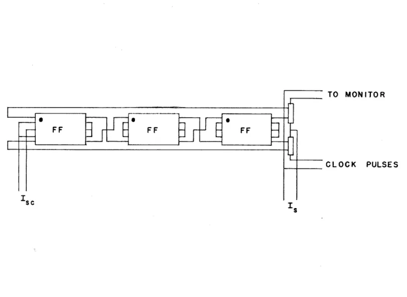
The clock for the computer as shown in Figure 19, consists of a number of flip-flops connected as in the delay circuit of Figure 5, with feedback from the output of the last flip-flop to the input of the
first. In particular the ONE output goes to the ZERO input while the ZERO output goes to the ONE input. Output pulses are obtained through the use of a pair of cryotrons whose controls are in the
feedback loop. This permits the use of a separate current source Isc which is used to control the pulse repetition frequency. Of the pair,
one cryotron provides a means of monitoring the frequency, while the other provides the computer with pulses.
4. 10 THE CLOCK GATES
The clock gates are shown in Figure 20. Clock pulses enter on the line marked CLOCK PULSES from the clock itself, and go to the output gates of FF1, the START, STOP (ST, SP) flip-flop. The pulses are steered either to the steering gates of FF2 or to the pulse return line via the stop indicator ({SI) line. The output gates
of FF., the HALT flip-flop, steer the pulses either to FF3, the Instruction-Execution-cycle flip-flop, or to the pulse-return line via the HALT INDICATOR (HI) line and the ONE output gate on FF4. FF steers the pulses either to an instruction cycle (ICP) or an
3
execution cycle (ECP). If a HALT command occurs, the halt pulse sets FF2 to the ONE state, diverting the clock pulses to FF .
OSEC and OSIC are activated from external push button switches and perform Operate Single Execution Cycle and Operate Single Instruction Cycle respectively. The line labeled CONTINUE (C) is activated by an external push button switch for continuing the program after a halt instruction.
-45-FF 0 0 F F
:1
l
F FI
E
FF IIs c
TO MONITOR CLOCK PULSESIs
FIGURE 19 CRYOTRON CLOCK
II
LT H IH FF2 H I ICP-F ICP-F 3 -
ECP-FIGURE 20 CLO CK GATES
FF1 CLOCK PULSES SI C OSE C OSIC ST SP HA sic SEC
ICP-FF F4 FF 5EP -- -r
-48-4. 11 THE OVERFLOW REGISTER
The overflow register is the name given the circuit which will give an indication of and store an overflow should it occur. An overflow is detected by checking the sign of the accumulator against the occurance or non-occurance of an end-around-carry in the Adder. The circuit is shown in Figure 21. The sign of the A register and the end-around-carry of the Adder, both of which are d-c levels are fed to the controls of the logic cryotrons. (YEOC stand for YES END
AROUND CARRY; NEOC stands for NO END AROUND CARRY) I
s
enters at the junction of the sign gates, and accordingly goes to another set of gates to determine the condition of the end-around-carry, from which it then sets the flip-flop to ONE if an OVERFLOW has occured, and ZERO if there was no overflow. There are two input command
lines to the register, TRANSFER ON OVERFLOW and TEST FOR OVERFLOW which are labeled 13 and 14 respectively in the diagram. A pulse to the TRANSFER ON OVERFLOW command line goes to a
set of output gates on the flip-flop and will either advance the instruc-tion counter or read the ADDRESS in the control into the instrucinstruc-tion counter according to whether or not an overflow is stored in the
flip-flop. A pulse to the TEST FOR OVERFLOW command line goes
to a set of output gates on the flip-flop and will either return to the pulse source or cut the main clock (stop) off.
One set of output gates is used for a visual indication of OVERFLOW on the panel of the computer. This line goes to the overflow indicator amplifier. A third command line labeled 22 in the
diagram is used to set the overflow register to ZERO; that is, to set it to the NO OVERFLOW state.
4.12 PRODUCT SIGN DIGIT REGISTER
SIGN-SI
SIGN +
YEOC
NEOC
13 , ADVANCE PROGRAM COUNTER
READ ADDRESS INTO PROGRAM COUNTER
14 RETURN
STOP
TO PANEL OVERFLOW is
READ SIGN INTO STORAGE PULSE F TO A REGIST -- COMPLEMENT COMPLEMENT NECESSARY IF LINE SIGN DIGIT ER LINE
7
--sm=1 I
SA=z SM ----MSM=O|
-51-consists of a network of gates whose controls are driven by the
outputs of the A register sign digit order, and the M register sign
digit orde.r. At the occurance of a READ SIGN INTO STORAGE pulse
the product sign digit is stored in the flip-flop. At the completion of the multiplication operation a pulse to the output gates of the flip-flop will complement the A register if the product is negative.
4. 13 COMMAND LINE SELECTION MATRICES 4.131 ADDITION
When a d-c level from the instruction selection matrix is placed on the ADD line as shown in Figure 23, the complementation circuit permits the clock pulses to enter the counter. The counter is initially set to ZERO and while in this state the zero output prevents pulses from other selection matrices from having more than one path. The first count unlocks these lines and source current is applied to
CML 14, which tests for overflow. The next count pulses CML 12, which reads the memory into the Bus. The third pulse reads the
Bus into the B register. The fourth pulse performs three functions: it reads the A register into the ADDER, the B register into the ADDER, and pulses the Carry Line to perform addition. These are CML 7, CML 17, and CML 18 respectively. The next pulse performs the two operations of reading the adder into the A register, and advancing the instruction counter, which are labeled CML 1 and CML 10 respectively. The last pulse is CML 15 and switches the clock to the instruction cycle. The counter is reset to ZERO during part
of the INSTRUCTION CYCLE.
4.13-2 SUBTRACTION
The command line selection matrix for subtraction is identical to that of the addition matrix of section 4. 13-1 with the exception of
ADD C J. s CLOCK PULSES COUNTER
- - - -
- -
-E-El
IsCOMMAND LINE SELECTION MATRIX FOR ADDITION
CML 14 CML 12 CML 16 CIVL 7 CML I7 CML 18 CML I CM L 10 CML 15 1
W,
FIGURE 23SUBTRACT C Is CLOCK PULSES COUNTER
-I-I
IsFIGURE 24 COMMAND LINE SELECTION MATRIX FOR SUBTRACTION
CML CML CML CML CML CM L CM L CML CML 14 12 19 7 17 18 1 10 15