Cell Modulated dc/dc Converter
by
James Raymond Warren III
Submitted to the Department of Electrical Engineering and Computer
Science
in partial fulfillment of the requirements for the degree of
Master of Engineering in Electrical Engineering and Computer Science
at the
MASSACHUSETTS INSTITUTE OF TECHNOLOGY
September 2005
©
James Raymond Warren III, MMV. All rights reserved.
The author hereby grants to MIT permission to reproduce and
distribute publicly paper and electronic copies of this thesis document
in whole or in part.
H
AUG 14
2006
LIBRARIES
A uthor ...
...
Department of F itrical Engineering and Computer Science
August 1, 2005
Certified by...
...
BARKER
David J. Perreault
Associate Professor
Thesis Supervisor
Certified by.. .
...
Ti othy C. Neugebauer
Sr. Memberf*4e
echni al Saff,'C.
Dr per Laboratory
eTVPsSxupervisor
Accepted by... .C.m
Arthur C. Smith
wombu
Cell Modulated dc/dc Converter
by
James Raymond Warren III
Submitted to the Department of Electrical Engineering and Computer Science on August 1, 2005, in partial fulfillment of the
requirements for the degree of
Master of Engineering in Electrical Engineering and Computer Science
Abstract
A very high frequncy converter roughly based on a class E topology is investigated for
replacing a conventional boost converter circuit. The loss mechanisms in class E in-verters are characterized, and metrics are developed to aid in device selection for high frequency converter. A (30 MHz) converter is developed based on a modified class
E inverter, single diode rectifier, and cell modulation control architecture based on
the Fairchild Semiconductor FDN361AN MOSFET identified by the device selection metrics. In addition to meeting the output specification of 1 W to 2 W, the converter has the ability to deliver up to 3W over its entire input voltage range of 3.6V to 7.2V. Converter efficiencies were realized ranging from from 71% to 81%. Finally, converter transient response to a 2:1 load step did not even exceed the transient ripple of the converter, approximately 100mV. Higher frequency design allowed for decreasing the magnitude of passive values, and in turn their corresponding physical size. Smaller magnitude components reduced the energy storage in the circuit, allowing for the im-proved transient response. A potential application for this reseach include integration of the circuit and/or passive components for further minitaurization. Potential ap-plications that could take advantage of the significantly improved transient response are circuits facing load transients, or applications designed to actively modulate their supply voltage or power.
Thesis Supervisor: David J. Perreault Title: Associate Professor
Thesis Supervisor: Timothy C. Neugebauer
Acknowledgments
This thesis was prepared at The Charles Stark Draper Laboratory, Inc. under
Con-tract No. CON05000-2, GB Draper Laboratory Fellow Support.
Publication of this thesis does not constitute approval by Draper or the sponsoring
agency of the findings or conclusions contained herein. It is published for the exchange
and stimulation of ideas.
James R. Warren III
I owe nothing more than to my wife Jes, who has been through this process by
side. Thank you for everything.
I would like to thank everyone at MIT that has helped me through this process.
My advisor, Prof. David J. Perreault, deserves accolades for the lengths lie went
to in supporting me. Thank you for your patience and your help. Juan Rivas and
David Jackson stood next in line for my questions when I headed to LEES. Thank
you for sharing your wisdom with me. Group meetings also introduced me to Olivia
Leitermann and Yehui Han who watched my thesis grow. To everyone else in LEES
who stopped by with kind words, my thanks.
I would like to reiterate my thanks to C.S. Draper Laboratory for supporting my
thesis. I also appreciate the broad freedom that my supervisor, Seth Davis, allowed
me in choosing a topic. Timothy Neugebauer, my thesis supervisor, was a great help
through the process. My cube farm/conference room/office mates, James Noonan
and Nick Nestle, helped keep the process light along the way. Best of luck guys.
Finally, Jay Bruso was an outstanding mentor. Thank you for everything.
Finally, I would like to thank my parents for their support throughout my
ed-ucation. You gave given me great tools to head into the world, and I will always
Assignment
Draper Laboratory Report Number T-1537
In consideration for the research opportunity and permission to prepare my thsis
by and at The Charles Stark Draper Research Laboratory, Inc., I hereby assign my
copyright of the thesis to The Charles Stark Draper Laboratory, Inc., Cambridge,
Massachusetts.
Contents
1 Introduction 15
1.1 Research and Background . . . . 16
1.2 Thesis Objectives and Contributions . . . . 18
1.3 Organization of Thesis . . . . 19
2 Losses in Class E Inverters 21 2.1 Class E Design Equations . . . . 21
2.1.1 Simplifying Assumptions . . . . 21
2.1.2
Q
L . . . . . . . . . 222.1.3 Output Power, P . . . . 23
2.1.4 Conduction Loss . . . . 23
2.1.5 Resonant Tank . . . . 25
2.2 Insights from Simplified Design Equations . . . . 26
2.2.1 Output capacitance limits . . . . 26
2.2.2 Simplified Expression for Output Power . . . . 26
2.3 Gating Losses . . . . 27
2.3.1 Traditional "Hard Switched" Gate Drive Losses . . . . 27
2.3.2 Resonant Gate Drive . . . . 28
2.4 Total Device Losses . . . . 29
3 Switching Device Selection 33 3.1 Maximum RON . . . . . .. . . . . . 34
3.3 Device Characterization . . . . 35
3.4 Finalized Device Selection . . . . 38
4 Class E Inverter Design 39 4.1 Loaded
Q
. . . . 394.2 Load Resistance . . . . 40
4.3 Resonant Tank Parameters . . . . 40
4.4 PSPICE Simulation of Class E Inverter . . . . 41
5 From Inverter to Converter 43 5.1 Tank Transformation . . . . 44
5.2 R ectification . . . . 45
5.3 Prototype Cell . . . . 46
6 Resonant Gate Drive 51 6.1 Multi-Stage Gate Drive . . . . 51
6.1.1 O scillator . . . . 51
6.1.2 CMOS Inverter Drive Stage . . . . 53
6.2 Resonant Gate Drive Circuit . . . . 54
6.2.1 Basic Resonant Gate Drive Circuit . . . . 54
6.2.2 Improved Resonant Gate Drive Circuit . . . . 56
6.2.3 Effective Gate Capacitance . . . . 57
6.2.4 Effects of Reverse Capacitance . . . . 58
7 Cell Modulation Control Architecture 59 7.1 General Theory . . . . 59
7.2 Feedback Network . . . . 60
7.3 Enable/Disable Circuit for the RF Converter . . . . 61
7.4 Hysteresis Band . . . . 62
8 Experimental Results 65
8.1 Open Loop Converter Efficiency . . . . 66
8.2 Cell Modulated Converter Efficiency . . . . 66
8.3 Cell Modulation Operation . . . . 67
8.4 Output Voltage Ripple . . . . 68
8.5 Load Step Response . . . . 69
9 Conclusions 79 9.1 Research Developments . . . . 79
9.2 Converter Development . . . . 80
9.3 Potential Future Work . . . . 80
A PSPICE Code 81 A.1 Class E Inverter Simulation . . . . 81
A.2 Converter Cell Simulation . . . . 82
A.3 Resonant Gate Drive Simulation . . . . 84
A.3.1 Input to Gate AC Simulation . . . . 84
A.3.2 Drain to Gate AC Simulation . . . . 86
B Circuit Schematic 89 B.1 Schematic . . . . 89
B.2 Bill of Materials . . . . 89
C PCB Layouts 93 C.1 Component Side Copper . . . . 93
C .2 Silk Screen . . . . 94
C.3 Solder Side Copper . . . . 94
List of Figures
2-1 2-2 2-3 2-4 2-5 3-1 3-2 3-3Class E Inverter Topology [1]. . . . .
Totem Pole Gate Drive Circuit. . . . . Resonant Gate Drive Circuit . . . . Loss Mechanisms in FDN361AN vs. Frequency.
Loss Mechanisms in FDN361AN vs. Pt . . . .
MOSFET Capacitances . . . .
Normalized Device Losses vs. Frequency . . . . Loss Mechanisms in FDN361AN . . . .
4-1 Class E Inverter Circuit for PSPICE Simulation . . . . 4-2 Class E Inverter Waveforms from PSPICE Simulation . . . .
5-1 Tank Transformation . . . .
5-2 Converter Cell . . . .
5-3 Converter Simulation Waveforms . . . .
5-4 Unregulated Cell Waveforms . . . .
5-5 Prototype cell power and drain efficiency (excluding gating loss power)
6-1 Multistage Resonant Gate Drive Circuit . . . . 6-2 Relaxation Oscillator Circuit . . . .
6-3 CMOS Inverter Structure . . . .
6-4 Basic Resonant Gate Drive Circuit . . . . 6-5 Improved Resonant Gate Drive Circuit . . . .
. . . . 21 . . . . 27 . . . . 28 . . . . 30 . . . . 31 . . . . 36 . . . . 37 . . . . 38 41 42 45 46 48 49 50 52 52 53 55 57
7-1 Cell Modulation Architecture Block Diagram . . . . 60
7-2 Cell Modulation Control Schematic . . . . 60
8-1 Prototype Converter Cell . . . . 65
8-2 Converter Efficiency . . . . 68
8-3 Cell Modulation Behavior . . . . 69
8-4 Cell transient behavior, V,n = 5.0V and Rload = 24 Q . . . . 70
8-5 Output Ripple of LM7231Y Demonstration Board . . . . 71
8-6 Converter Output Voltage Ripple . . . . 72
8-7 Converter Output Voltage Ripple, Meaurement Bandwidth = 20 MHz 73 8-8 Load Step Response of LM2731Y Demonstration Board . . . . 74
8-9 Load Step Response of LM2731Y Demonstration Board . . . . 75
8-10 Load Step Response of Cell Modulated Converter . . . . 76
8-11 Ripple Resonse to Load of Cell Modulated Converter . . . . 77
B-i Converter Schematic . . . . 90
C-1 Solder Side Copper, 2X Magnification . . . . 93
C-2 Component Side Silk Screen, 2X Magnification . . . . 94
C-3 Solder Side Copper, 2X Magnification . . . . 95
List of Tables
2.1 Class E Inverter Parameters . . . .
3.1 Characterized Devices . . . .
5.1 Tank Values from Transformation at
f,
= 30 MHz . . . . 5.2 Unregulated dc-dc Cell Efficiency (Gating loss power not included)8.1 Open Loop Converter Power and Efficiency . . . .
8.2 Prototype converter efficiency . . . .
8.3 Cell Modulation Frequencies . . . .
B.1 Bill of Materials for Converter . . . .
22 36 45 47 66 67 68 91
Chapter 1
Introduction
DC/DC power converter design encompasses tradeoffs between power density, de-fined as converter power relative to converter size, and efficiency. The problem of power density translates to miniaturization when applied to lower power (< 10 W) range switching converters. The sizes of passive components in a low power reg-ulator dominate over the size of the switching devices themselves. Moreover, the numberical values and stored energy in these passive components directly determine achievable transient response; lower valued passive components lend themselves to faser transient response. The switching frequency is the key to sizing the passives; increasing frequency can lower the size of the devices and improve achievable tran-sient performance. This is not without the challenge of mitigating switching, gating, and magnetic core losses, which scale with frequency, and reduce overall converter efficiency.
The primary application for this research is to reduce the size and improve the transient response of a power supply currently implemented as a boost converter based on a National Semiconductor LM2731. The application is to boost and regulate a battery voltage supply over the discharge cycle of the cells. While the chip is efficient and small, operating at a switching frequency of 1.6 MHz or 0.6MHz depending on the version, it requires relatively large exterior passive elements, including the input and output capacitors and the boost inductor. Moreover, its response speed and transient output voltage variations (e.g. in response to load transients) is limited by the energy
stored in the passive components (especially the inductor) and its switching frequency. The design objective is to increase the switching frequency significantly to the vhf range (30-300MHz) in order to reduce the total size of the passive components and to provide better dynamic performance (e.g. smaller and shorter output voltage transients during load changes). A cellular control architecture is investigated to
apply an optimized rf cell to the necessary load range [2, 3, 4, 5, 6, 1, 7, 8, 9, 10, 11,
12, 13, 14, 15].
1.1
Research and Background
A traditional direct converter is designed to meet wide load ranges by varying its
duty cycle. The load range, which can easily exceed an order of magnitude, limits the extent to which the converter topology can be optimized. A recent approach is to develop a control structure around optimized radio-frequency converter cells. While an individual cell is designed for a narrow load range, the control structure adapts to wider ranges by modulating the cell on and off over time, and/or by changing the number of cells used to supply the load [2].
In this strategy, regulation of the output is provided by modulating the cells in the time domain, with an output filter to smooth the resulting power pulsations and provide the desired average output power. The benefit is that the sizes of the converter magnetics are determined by the switching frequency, which can be extremely high without sacrificing efficiency. There is thus the opportunity to reduce the size of the largest passive component in the system. The output filter (e.g., a capacitor) still needs to provide filtering at the lower modulation frequency, but often times it is sized
by other system requirements as well. Moreover, the high switching frequency and
low stored energy in the magnetics can yield exceptionally fast transient performance. For low power converters, the cell modulated cellular architecture can be reduced down to a single cell using on-off, or bang-bang, control. The general approach is that an output filter is used to store and filter the energy which is regulated by modulating an optimized cell with a varying on-off duty cycle to meet the load requirement.
While the output requirements of the entire architecture will size the output filter, the intermediate passives can be sized to the optimized cell.
In this strategy, the power conversion is accomplished using a resonant cell op-erating at very high switching frequencies. As the switching frequency is increased, the power losses associated with each switch transition accumulate. This has lim-ited traditional direct converter switching frequencies in order to preserve efficiencies. Switching loss occurs when a switch transitions from a high current state (on) to a high voltage state (off). Neither the current or voltage changes instantaneously; the switching loss comes from their product during the switching transition. In order to increase switching frequency without sacrificing efficiency, a method of Zero Voltage Switching (ZVS) should be implemented. By ensuring that the voltage across a switch remains at or near zero during its switching transition, the power dissipation can be minimized [3, 4].
High frequency analog design is an area with established design principles. As switching frequencies rise, these RF principles are very applicable to power electronics design. Moving towards a more sinusoidal gating signal and resonating charge on and off the gate, as opposed to a square wave drive, lowers the gating power loss that can limit high frequency operation [3, 2, 5, 6]. A resonant converter is a solution that takes advantage of these RF design principles. Multi-stage self resonant amplifier circuits that do not require a drive oscillator can be effectively employed in this context.
The implementation pursued in this thesis is the use of a converter based on a resonant class E inverter [1, 7]. The class E inverter circuit is combined with a single diode rectifier to create a full dc/dc converter with minimal part count and size. A cell modulation architecture in the form of bang bang control is used to regulate the output voltage.
The benefit of a cell-modulated control architecture is that an optimized conver-sion cell can allow for switching frequencies that are orders of magnitude higher than a traditional direct converter. The tradeoff is in design complexity over a direct con-verter in both the topology of the concon-verter cell and the architecture of the control system. The benefits, however, are that resonant techniques can be applied to
re-duce switching losses, leading to higher frequencies, smaller passive components, and improved converter transient response.
1.2
Thesis Objectives and Contributions
The objective of this thesis is to design a dc/dc converter that meets the following specifications.
" Input voltage range: 3.6 to 7.2 volts
" Output power range: 1W - 2W
* Output current range: 150mA to 250mA
* Output voltage: 7V
The current solution of a National Semiconductor LM2731 Boost Converter op-erating at 0.6 MHz will serve as a point of reference for the contributions of this thesis. The ojective is to decrease passive sizes and improve transient performance
by pursuing a topology that allows for a high frequency cell modulated converter. A loss analysis of class E inverters is developed using design equations from [1].
The loss analysis encompasses both device conduction loss as well as gating losses associated with driving the transistor. This loss analysis provides the basis of metrics for device selection for high frequency power converters.
A device search is conducted to identify candidate devices for a low power, high
frequency resonant converter. Devices from 3 manufacturers were compared both on the basis of published specifications as well as data from experimental characteriza-tion. This information allowed for a device to be selected for a converter design.
Based on the selected device, a converter topology is developed based on a modified class E inverter combined with a single diode rectifier. PSPICE simulation is used to analyze and develop the circuit. A prototype converter is implemented to confirm the desired efficiency due to conduction loss in the power stage.
A multi-stage resonant gate drive circuit is developed to provide a sinusoidal drive
signal with dc offset at the gate of the selected device. The circuit includes a second
LC tank to reduce device stress on the switching devices providing the gate drive.
Finally, the circuit addresses the need to mitigate self oscillating behavior due to Crs providing feedback from the drain to gate.
A cell modulation control architecture is implemented to control the high
fre-quency converter cell. It also provides voltage regulation at the output. The control architecture allows for near instantaneous transient response time.
Finally, the full converter cell is prototyped and characterized. Initial open loop efficiency is measured to asses the maximum power capacity of the device at the specified output voltage. Then, the closed loop system is characterized within the specifications for efficiency, cell modulation characteristics, and transient response to
load steps.
1.3
Organization of Thesis
Chapters 2 and 3 develop the loss analysis of class E inverters and an approach for evaluating candidate switching devices for high frequency resonant converters. Chapters 4 and 5 develop the power stage of a dc/dc converter based on a class E inverter.
Once the high power stage is designed and protoyped, Chapter 6 develops a multi-stage gate drive circuit. It is followed by a development of the cell modulation control architecture in Chapter 7.
Experimental results from the full dc/dc converter comprise Chapter 8. Finally, Chapter 9 summarizes the contributions of this thesis and expounds on directions the work could be extended.
Chapter 2
Losses in Class E Inverters
2.1
Class E Design Equations
In order to develop a tractable design for a class E inverter, design equations from
[1] are introduced. The classic class E inverter topology is presented in Figure 2-1.
Design equations have been documented for this topology to set up class E operation
[1]. Table 2.1 contains an explanation of the parameters for the class E inverter.
Li
L 2C2
02VC
+
1
R
CCT
Figure 2-1: Class E Inverter Topology [1].
2.1.1
Simplifying Assumptions
Some simplifications clarify the design equations without sacrificing significant con-trol of the parameters. The following assumptions are that parasitic resistances are negligible, the choke inductance is large, QL is large, and the fall time of the switch current at turn off tf is signinficantly shorter than the switching period. These results
Parameter Description
f
Switching frequencyVcc Supply voltage
VI Switch voltage drop L, Choke inductor
L2 Resonant tank inductor
C1 Output capacitance across switch
C2 Resonant tank capacitor
R Load resistance attached to tank
RON Switch on-state resistance
Rioad Effective load resistance seen by converter Table 2.1: Class E Inverter Parameters
of these assumptions are
ESRL2=
ESRC
2 =ESRc
QL
tf
=0 = 00 = 00<< T
2.1.2
QL
QL
is theQ
of the resonant tank in the class E inverter. The L subscript stands for"loaded
Q".
27rf L2
QL =
R
(2.5)It is a free choice variable subject to the constraint
QL > 1.7879 (2.6)
Large QL coincides with a tank with a high purity sinusoidal output. A low
QL
is desirable for power converter designs utilizing the class E topology. A lower QL reduces the magnitude of the energy resonated in the tank, which in turn reduces conduction losses associated with the parasitic resistances of L2 and C2 [2].
(2.1) (2.2)
(2.3)
2.1.3
Output Power, P
Design equations are developed based on a least squares fit to tabulated values for
design parameters in terms of QL and supply voltage.
f(QL)
is the fit equation.(VCC _ Vo 2
P
=(c o 2f(Q L) (2.7)
For a second order polynomial fit, the fit equation is
[11
0.451759 0.402444 (2.8)
f(QL)
=1.001245- QL2(28Q L
QL
Therefore output power is
(CC
_Vo)--2~~0415
.044
V) 2
2
1.001245 -0.451759
-
(2.9)
R
_
+ 1.
QL
L5
The switching devices examined for this design were all MOSFETs, so Vo = 0.
Under the simplifying assumption of
QL
= oo, all of the higher order terms off(QL)
drop out. The simplified equation for output power is then
_(Vc)[ 1 ]Q
(V)22
0.5775 CC)2 (2.10)
R
Rearranging Equation 2.10 provides a calculation of the necessary load resistance for the inverter in terms of desired output power and supply voltage.
R
= 0.5775.(V
0C) 2 (2.11)P
2.1.4
Conduction Loss
Drain efficiency, 'rD, is defined as the output power divided by the dc input power, neglecting gate drive power losses. It is often used as a measure of performance in rf power amplifiers. Existing expressions for calculating drain loss in [1] will be used to
compute conduction loss in the inverter switch.
In order to calculate the drain efficiency, two new parameters are introduced. RLOAD is an effective resistance term introduced in [1] for calculating drain efficiency.
RLOAD = R - ESRL2 - ESRC2 - 1.365 - RON - 0.2116. ESRc (2.12)
A is a function of the fall time compared to the switching period, and is defined as
A = (I
+
0.82) tI) (2.13)Using these new parameters, the drain efficiency TID is calculated as
[1]:
RLOAD
RLOAD + ESRL2+ ESRc2+ 1.365. RON + 0.2116. ESRc1
(27A
A)212 -0.01 12
(2.14)
Combining Equation 2.14 with Equation 2.12 reduces to
RLOAD
7D R (2irA)
2
- 0.01
12 (2.15)
The constant 0.01 is designed to incorporate conduction losses associated with the RF choke, L, [1]. In order to focus on losses associated directly with the switching device, this loss will be dropped. Finally, by applying the simplifying assumptions of Equations 2.1-2.4, the parameters used to calculate iD reduce to
RLOAD = R-1.365-RON
A A== t = 0
(2.16)
(2.17)
Combining these approximations leaves the drain efficiency assuming only con-duction loss in the switch
RLOAD
D R + 1.365- RON
R
-1.365-
RONR
= 1
-
1.365- RONR
(2.18)Combining Eqns. 2.11 and 2.18 gives
P
'D = 1- 1.365. RON O.5775 -(Vcc) 2 O P RON =1
- 2.363 -(VO)
(VCC)2 (2.19)This is equivalent to saying that device conduction loss normalized to dc input power is
P
Normalized Conduction Loss
= 2.363-
(VCC) 2RON (2.20)For given system parameters of input voltage and output power, normalized con-duction loss is independent of frequency.
2.1.5
Resonant Tank
Design equations are developed for the resonant tank parameters C1 and C2 using
the same fit technique described in Section 2.1.3 [1]. The output capacitance across the switch is 1 Cf )
0.99866+
27rf R
(i _ + ) 2 0.91424QL
1.03175)Q2
+ 0.6 (27rf)2L1 (2.21)Incorporating Equation 2.11 into Equation 2.21 and simplifying it with QL
=
oand L, = oc gives 1 27rf R +1) 1
27rf R
+1)
1 = 0.02918-fR .02918 P .5775 f(VC) 2(.99866+
(0.99866) 0.91424 QL 1.03175) 0.6 (27rf)2Li= 0.05053 -f
c
(2.22) f (VCC)2The equation for C2 does not easily simplify under these same assumptions. The
full equation should be used once the free choice variable QL has been chosen as
follows
C2= 1(100121 1.01 (2.23)
20rf R
QL~0.104823
+L
-1. 787 9 (27(2)220Finally, the value for L2 will follow from the choice for QL- Under the simplifying
assumption of
QL
= oc, L2 does not have a significant value. Its calculation will alsobe reserved until after design decision for a practical QL is chosen, and calculated as
L2 = (2.24)
27rf
2.2
Insights from Simplified Design Equations
2.2.1
Output capacitance limits
Equation 2.22 offers an insight into the applicability of a given switching device to a class E inverter. It helps place an upper bound on what an acceptable output capacitance is for a given application of power and frequency. If the device output capacitance is lower than needed to achieve a desired power at a specified frequency, external capacitance can be added to the specification.
P
C1 < 0.05053. (2.25)
f (VoC)2
2.2.2
Simplified Expression for Output Power
Rearranging Eqn 2.22 also gives an insightful equation for output power. It breaks down the class E capacity as a function of frequency, device capacitance, and input power.
This is a valuable equation because it immediately qualifies for a given frequency and input voltage, what power a device can deliver. It is useful for a first approxima-tion for design and for evaluating switching devices.
2.3
Gating Losses
2.3.1
Traditional "Hard Switched" Gate Drive Losses
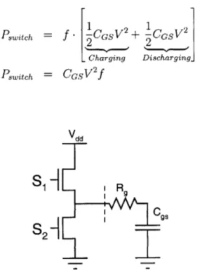
Traditional "hard switched" gate drive circuits the gate capacitor on each switching cycle. A is illustrated in Figure 2-2. In each switching charge the input capacitance of the switching
then turned off by sinking all of the charge on S2. This results in a total switching loss of [8]:
Pswitch
Pswitch
dissipate all of the energy stored on traditional totem pole drive circuit cycle, the circuit sources current to
device through Si. The MOSFET is
the gate capacitor to ground through
(2.27)
Vdd
gs
S C
Figure 2-2: Totem Pole Gate Drive Circuit.
= f [ICGSV2+ CGSV2
Charging Discharging_
= CGSV 2
2.3.2
Resonant Gate Drive
A technique to reduce the dominance of traditional switching losses at high frequencies
is to employ a resonant gate drive circuit. In one possible implementation, an inductor is added in series with the input capacitance, creating an LC tank, as shown in Figure
2-3. This allows charge to be stored in the tank and rung on and off of the input
capacitor. The tank is recharged using a push-pull output stage similar to the hard switching design. However, the totem pole drives the equivalent of a second order LC filter, instead of charging and discharging the capacitor on every cycle. The resultant loss mechanism is dissipation in any ESR associated with the LC tank, including the internal gate resistance.
V dd
L R
L3 |i
Cgs
Figure 2-3: Resonant Gate Drive Circuit
The resultant voltage at the gate is the fundamental of the switch frequency as filtered by the LC network, ideally a pure sinusoidal drive with a dc offset. Assuming a sinusoidal gate drive allows the calculation of the loss associated with driving the gate capacitance of a MOSFET. The approach is to calculate the current onto the gate, and then calculate the loss associated with passing that current through Rg, the ESR associated with C,.
Zc13 (2.28)
0tjw
the magnitude of the gate current may be calculated as:
|i| = 27rfCgsV sinwt (2.29)
and the mean-square gate current is:
i2 (27TfCgsV) 2
=
27r2f2C2sV2 (2.30)
2
RMS 2 g
The power dissipated in Rg is then
P = iRMSRg
= 27r2f 2C2sRgV2 (2.31)
Using Equation 2.10, the gating loss normalized to inverter power is: 27r2f2C2
R
V2Normalized Gating Loss = Ps 9 (2.32)
P
2.4
Total Device Losses
Eqns 2.20 and 2.32 can be summed to express the total normalized device loss in terms of device parameters RON, Cgs, and Rg and as a function of frequency f:
P 27r2 2C2 R V2
Normalized Device Loss = 2.363. (V) 2 RON+ gs g (233) Conduction Loss Gating Loss
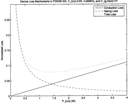
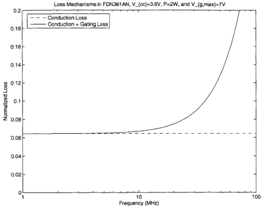
Figure 2-4 illustrates how the loss mechanisms in a single device vary versus fre-quency. The data for the plot comes from the device ultimately selected for the converter design. At low frequencies, conduction loss is the dominant factor. How-ever, as frequency increases, gating loss quickly becomes the limiting factor.
There is also an optimal output power for a given device at a fixed frequency and input voltage. This is because the normalized conduction loss factor increases linearly with output power for a fixed input voltage, while normalized gating loss
Loss Mechanisms in FDN361 AN, V_{cc}=3.6V, P=2W, and V_{g,max}=7V 0.2
- - - Conduction Loss
0.18-1 |Conduction + Gating Loss 0.16- 0.14- 0.12-0 -j 0.1 -E 0 Z 0.08 - 0.06- 0.04- 0.02-0 '. , 1 10 100 Frequency (MHz)
Figure 2-4: Loss Mechanisms in FDN361AN vs. Frequency
factor decreases. The power consumed via gating loss is constant for a set frequency and peak drive voltage, so as power output increases, the gating loss factor decreases. Fig 2-5 illustrates this concept.
The output power variation is created by assuming that an arbitrary amount of additional capacitance can be added in parallel with a device's Cds. A device's
Device Loss Mechanisms in FDN361 AN, V_{cc=3.6V, f=30MHz, and V_{g,max}=7V I I II I Conduction Loss - - - Gating Loss .... Total Loss -. - . 0.5 1 1.5 2 P_{out} (W) 2.5 3 3.5 4
Figure 2-5: Loss Mechanisms in FDN361AN vs. P,
0.25 F 0.21-0.15 0 z 0.1 0.05F 0' 0
Chapter 3
Switching Device Selection
This chapter considers inverter device selection for the power converter. The loss models of Chapter 2 are used to make quantitative decisions regarding device seection and converter switching frequency. The objective was to find commercially available MOSFETs that could be employed in an unconventional manner at higher frequencies. In order to develop a road map for the device search, the information commonly available for devices was considered. Equation 2.33 for device loss normalized to input power is restated here for reference
P
27r 2f 2 C28 RgV2Normalized Device Loss
= 2.363 2RON+ -(3.1)
(VCC) P
Conduction Loss Gating Loss
Four parameters primarily define the viability of a MOSFET for a high frequency switching application. RON, Cgs, Cds, and
R.
are the parameters of interest. Witha fixed input voltage and output power requirement, RON dictates the conduction loss in a device. Coss will next influence the switching frequency as determined by Equation 2.10; with that, it will affect the size of the passive elements. Coss can also serve as an indicator as to whether the device is oversized for the application. Finally, the gating losses in a resonant drive circuit are determined by Cgs and Rg.
Unfortunately, of the four parameters, only three of them are commonly disclosed on datasheets. Rg is the ESR associated with the gate terminal and a parasitic that is not usually included. This is understandable, considering the difference in loss
mechanisms between the traditional drive of Section 2.3.1 and the resonant drive structure of Section 2.3.2. Losses in traditional gate drives depend only on Cg, and peak drive voltage V; they are independent of the parasitic gate resistance R., so it is often left out of datasheets. Candidate devices must be selected without knowing R9 and then tested to evaluate R. and determine switching performance.
3.1
Maximum
RON
An initial polling of available devices was conducted. The selection criteria were looking for an RON that would allow for at most 5% conduction loss. Recalling Equation 2.20, the maximum RON must be evaluated at Vin,min and Pout,max for a chosen normalized conduction loss Pc:
RON
0.423
(Vinmin )2PC(3.2)
Pout,max
Calculating this for Vcc,min = 3.6V and Pout,max = 2W, with an allowed loss
Pc ~ 5%, gave the first selection criteria of
RON
< 0.15Q
(3.3)Any devices that exceeded this specification were disregarded. RON was initially considered at the typical operating point for a rough search. It was then refined by applying the temperature coefficient effect, which results in a larger RON as
temper-ature increases.
For the devices that met the RON requirement of Equation 3.3, two metrics were developed. One was the normalized conduction loss at a fixed frequency and output power. The other was the maximum frequency the device could be operated at with a conduction loss less than or equal to 5%. For this metric, the output power was assumed to be set by the device's output capacitance and operating frequency. In the case where the resultant frequency and output capacitance delivered power beyond the output specificiation, it was assumed that cell modulation could be employed
to regulate the converter. The final requirement for selection was the availability of devices for characterization.
3.2
Maximum Gating Loss
Within the available devices meeting the conduction loss requirement, the second focus was to identify devices with the potential for low gating losses. Unfortunately, the data sheets often do not contain the necessary information about device parasitics such as R.. Reliable estimates can not be calculated solely from the data sheets as a result.
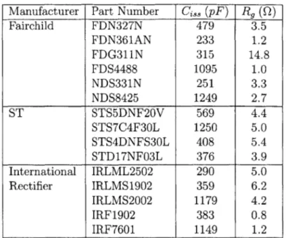
While gating loss varies linearly with Rg, it has a quadratic dependence on Cg,. This provides a guideline to search for devices with a low to moderate input capac-itance. This decision was based on the assumption that gate resistance is approxi-mately constant from device to device. With this assumption, the top two devices in each product line of three different manufacturers were selected for measurement. Package size was limited to requiring a surface mount package. Three manufacturers were identified for the candidate devices. The devices acquired for characterization are contained in Table 3.1.
The viable devices were acquired and characterized in order to effectively compare the potential losses of each device. For the purposes of the loss calculations, Cg, and R9 were determined experimentally while RON and C,,, (evaluated at the quoted operating point, typical V, ~ 20 V) were derived from the maximums on the data sheets.
3.3
Device Characterization
The capacitances of the MOSFET structure are significant circuit elements in the class E inverter topology. The parameters of interest are depicted in Figure 3-1. The datasheet capacitance measurements are related to the model capacitances by
Manufacturer Part Number Ciss (pF) R9 () Fairchild FDN327N 479 3.5 FDN361AN 233 1.2 FDG311N 315 14.8 FDS4488 1095 1.0 NDS331N 251 3.3 NDS8425 1249 2.7 ST STS5DNF20V 569 4.4 STS7C4F30L 1250 5.0 STS4DNFS30L 408 5.4 STD17NF03L 376 3.9 International IRLML2502 290 5.0 Rectifier IRLMS1902 359 6.2 IRLMS2002 1179 4.2 IRF1902 383 0.8 IRF7601 1149 1.2
Table 3.1: Characterized Devices
D
Cgd
GR
GW
_
I
Cds
gsS
Figure 3-1: MOSFET Capacitances
Ciss = Cgs + Cgd (3.4)
Coss = Cds + Cgd (3.5)
An HP 4395A in impedance analyzer mode was used to measure the input capaci-tance and its parasitic resiscapaci-tance. This device drives the device under test (DUT) with a sweep of input input frequency, measuring magnitude and phase of the response as a function of frequency. It then can extrapolate an individual measurement, such as
capacitance (based on the reactive component) or the series resistance (based on the
real component).
Measurements were performed between the gate and source of the device, with the
drain floating. As C,, is typically small compared to Cd,, their series combination
is approximately the same as if Cd, were shorted. An equivalent series RLC circuit
model was used to extract the parameters for gate resistance and any lead inductance.
Figure 3-2 contains loss data as computed by Equation 3.1 for four representative
devices. The best performing vertical devices from 3 manufacturers (ST, Fairchild
Semiconductor, and International Rectifier) are compared with a lateral device from
MACOM used for rf power amplifiers. The MACOM part is a significantly larger area
device and has a far larger package than the minitiaure packages focused on in the
device search. Moreover, this lateral device has special gate drive requirements (see
[9], [5]), making it impractical for use here. However, it helps illustrate how lower
gating loss allows for high frequency operation.
Device Losses, Vjcc}=3.6V, P=2W, and Vjg,max}=7V
0.2 MACOM LDMOS -- -FDN361AN 0.18 -- ... IRF1902 - STD17NF03L 0.16 - 0.14-S0.12-// 0.1 Z 0.08 - 0.06-0.04 -~ 0.02 ~ .... 0 0 0 100 Frequency (MHz)
Loss Mechanisms in FDN361 AN, \_{cc}=3.6V, P=2W, and V_.{g,max}=7V 0.2
- - - Conduction Loss
0.18 - Conduction + Gating Loss 0.16- 0.14- 0.12-0.1 -0 z 0.08 - 0.06- 0.04- 0.02-0 1 10 100 Frequency (MHz)
Figure 3-3: Loss Mechanisms in FDN361AN
3.4
Finalized Device Selection
Of the best performing miniature devices in Figure 3-2, the most efficient device at
very high frequencies was the Fairchild FDN361AN. While it has a higher conduction loss than the STD17NF03L, it has a combination of acceptable input capacitance and low gate resistance that allow for more efficient operation at higher switching frequencies. It will be used as the primary switching device for the development of the converter cell.
Figure 3-3 contains a closer look at the potential operating range of the FDN361AN. Using this information, and a target device efficiency of 90%, the switching frequency was selected to be
= 30 MHz (3.6)
With a switching device and operating frequency determined, the development of the converter cell could continue.
Chapter 4
Class E Inverter Design
This chapter addresses a first pass design of the inverter portion of the dc-dc converter. The loss calculations from Chapter 2 and the design equations from [1] were used along with the selected device of Chapter 3 to develop the following design. This inverter design is used as the initial basis for a full converter design, as described in the next chapter.
4.1
Loaded
Q
The simplifying assumptions of Equations 2.1-2.4 are too simple for a valid design. Specifically, assuming QL = o0 is insufficient for calculating the tank values L2 and C2 as denoted in Section 2.1.5. The design requirement for the equations from [1] is
QL
> 1.7879. Based on the discussion in Section 2.1.2 and [2], a low value ofQL
is desirable. The final design decision was to begin with(4.1) QL = 5
4.2
Load Resistance
Using the choice of
QL
from Equation 4.1, the load resistance R can be calculated. R is the load resistance that will deliver the maximum required power, 2.2 Watts allowing for losses, at the minimum input voltage, 3.6 V. It is computed by rewriting Equation 2.7 as(VCC - V)2-2~
R
= 2-2
2
f(QL)
=3.6 (0.576801) 1.001245 -0.451759
-0.402444
2.2QL
J
= 3.04Q
(4.2)4.3
Resonant Tank Parameters
The resonant tank design equations of [1], previously enumerated in Section 2.1.5 as Equations 2.21, 2.23, and 2.24 are restated here.
1 099866 0.91424 1.03175 0.6 27rf R (2 + 1)
I
QL9
(27rf)2L ( C2 = 1 1.00121 +1.0168
(4.4)27rf R
QL
-0.-104823
QL
-1.7879
(27rf)2L,
QLR
L2=
27f(4.5)
One simplification that will be carred over from Section 2.1.5 is the assumption that L= 00. The result of this is to disregard the second added term in the equations for C1 and C2. Using these equations and the values for QL and R from above results
in the calculated values
Ci,calc = 365 pF (4.6)
C2,calc = 470 pF (4.7)
Noting that the output capacitance of the selected device (FDN361AN) is approx-imately 50 pF, and approximating the calculated values to standard values results in the following tank values
C1
365 pF
-50 pF ~ 300 pF
(4.9)
C2
470 pF
(4.10)
L2
82 nH
(4.11)
4.4
PSPICE Simulation of Class E Inverter
Using the dsign values of Equations 4.2 and 4.9-4.11, a PSPICE simulation was de-signed to test the class E inverter, included in Appendix A.1. The model used an ideal switch in place of the FDN361AN, but its output capacitance was included in the value C, = 350 pF. The circuit of Figure 2-1 is repeated here as Figure 4-1 to
illustrate the circuit and component values used for the simulation. Figure 4-2 shows the resulting waveforms, demonstrating approximate class E operation for the circuit.
Note that effects of the MOSFET body diode are not included.
L L2 C
240 nH 82 nH
470 pF
R
VIN
- 1 3.04350 pF
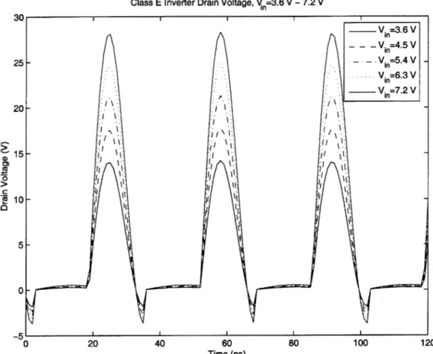
Class E Inverter Drain Voltage, V =3.6 V - 7.2 V 30 --- V. =3.6 V in V. in=4.5 V 25- - - V =5.4V V. =6.3 in V -_V. in=7.2 V 20 - 15-E510 -I i I 5- 0--5 II 0 20 40 60 80 100 120 Time (ns)
Chapter 5
From Inverter to Converter
The previous chapter considers the design of a class E inverter having approximately the correct power and operating frequency. This chapter considers the design of a full dc-dc power converter that is roughly based on this first pass inverter design.
To construct a dc-dc converter based on a class E inverter, it is necessary to rectify its AC output. An RF rectifier and matching network can provide this AC to DC conversion [10,1 1, 6, 3, 12, 13, 14, 2, 5]. However, in an effort to minimize the number of components, a simpler rectifier was investigated.
In a traditional class E dc/dc converter, the load resistor is replaced by an RF rectifier network. This network typically looks resistive to the LC tank, meaning it has a minimal reactive component in its impedance, or its reactive component is absorbed as part of the tank or matching network. Current gets delivered out of the
LC network into the "resistor" and then the tank is recharged from the input on the
next switching cycle. An output filter maintains a constant DC output with a low
AC ripple.
A new rectifier was designed that would allow energy to be drawn out of the tank
on each cycle, while also minimizing the number of components used. The topology is roughly based on a class E converter with a transformed tank. A diode connecting the tank to the dc output provides the means for energy removal. Analysis of the circuit with this rectifier is complex due to the nonlinear asymmetric behavior of the diode rectifier [11]. The system was refined using computer simulation to tune the
minimal number of components to meet the output requirements. The resultant tank values for a series class E inverter are the first column of Table 5.1.
5.1
Tank Transformation
The class E inverter developed in Chapter 4 served as the starting point for the dc-dc converter. Modifications to the topology allowed for the application of a simple rectifier with a single diode. The tank must be transformed from a series LRC combi-nation to a tank with an L in series with the parallel combicombi-nation of R and C. L and
C create the resonant tank, and R is the dissipative element. The resistor is replaced by a diode recitifier, which siphons energy and charge out of the tank. This section
develops the tank transformation.
Assuming that the tank current in a class E inverter is sinusoidal follows from the assumptions the design equations in Chapter 2. For a fixed operating frequency, the series LRC tank can be transformed to a tank with an inductor in series with the parallel combination of an R and C. The inductor is still a series element, so its value remains constant. What remains is a series to parallel transformation of the RC network, illustrated in Figure 5-1. The impedance equations for each structure are:
1j
ZSeries = + Rs = Rs - (5.1) jU)C2,s WC2,s1
Rp jwR 2C 2,P
Zparallel = . |Rp = -P(5.2) jWC2,P (wRpC2,p)2 + 1 (wRpC2,p)2 + 1To accomplish this transformation, equating the real and imaginary parts of the two transfer functions results in the following two equations in two unkowns. These can be evaluated at the operating frequency w = 27rf8. Table 5.1 contains the initial
series LRC tank values, and their transformed values for the new parallel RC inverter.
R = + (5.3)
C
ZE
j
2,S IRsSeries RC
Figure 5-1: Element L2 C2R
Z
C2,PParallel RC
Tank Transformation Series Parallel 52 nH 52nH470 pF 438 pF
3.04 Q 45 QTable 5.1: Tank Values from Transformation at
f,
= 30 MHzC2,P
1
Re RsC
2,sw
2(5.4)
5.2
Rectification
The result of the transformation described in the previous section allows for a simple rectifier. The load resistor R is what removes energy from the tank, which is the desired effect of the rectifier as well. The load resistor is replaced by a single diode feeding into a capacitive dc output filter. It is assumed that the output of the converter will be regulated to sit at a fixed voltage, enabling the capacitive output filter to be treated as a constant voltage. This topology is illustrated in Figure 5-2. As the diode capacitance is between the output of C2 and a constant dc node which serves as an ac ground, its capacitance can be absorbed into C2.
The diode acts as an uncontrolled switch. When the voltage across C2 swings
above the output voltage, the diode will conduct and draw charge out of the tank and into the output filter. The switch will continue to exhibit the zero voltage switching of the class E inverter (measured across C1) as its ouptut rings down prior to transition.
L 1 L 2
D
VIN C C 2 VOUT
Figure 5-2: Converter Cell
This comes from the LC tank that L2 forms with the capacitance across the output
of the switch C1.
The result of replacing the load resistor R with a diode is illustrated by the wave-forms in Figure 5-3. The drain waveform and the waveform across the tank capacitor
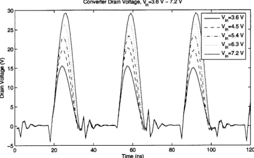
C2 are illustrated. The duty ratio of the diode is effected by C2 as it will determine the slope of its output voltage during the time when the diode is off. Adjusted tank values were determined using PSPICE to ensure zero voltage switching and to meet the output power requirements. Standard values were chosen for all components so that analysis could carry into prototyping directly. Manufacturer models were used for the MOSFET (Fairchild FDN361AN) and diode (Fairchild MBR0520L). The tank component values are
L, = 240 nH (5.5)
L2 = 56 nH (5.6)
C1 = 220 pF (5.7)
C2 =
220 pF
(5.8)The waveforms in Figure 5-3 was generated using these values in the circuit of Figure
5-2. Appendix A.2 contains the PSPICE files used.
5.3
Prototype Cell
The circuit simulated in the previous section was prototyped to confirm its viability for a final design. The purpose of the prototype was to confirm the operation of
the topology, and measure the conduction losses associated with it. The gate drive was provided by an external power amplifier driving the gate with a sinusoidal drive.
Gating losses are not included in this section.
One purpose of the prototype was to confirm that zero voltage switching could be achieved to prevent excessive dissipation at switch transitions. Figure 5-4 shows the drain voltage measured for operation across the input voltage range. Acceptable
switching behavior is achieved over the operating range.
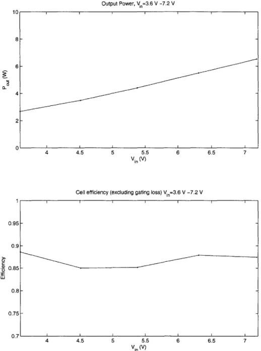
For purposes of testing the power stage design, the prototype converter was loaded with Zener diodes to maintain a constant output voltage. The converter was tested with 7.5 V Zeners capable of handling the power expected based on the simulations of the previous section. Loss associated with the conduction and switching loss was the main measurement taken from the prototype. The gate was driven by an external source, and power delivered to the gate is not accounted for here. Table 5.2 contains the measured drain efficiency data, and it is graphed in Figure 5-5. As can be seen, good drain efficiency (l7D = Qi-) is achieved over the input voltage range.
Vin 'in Pin Vout Iout Pout 77D
3.60 0.84 3.02 7.24 0.370 2.68 0.886
4.51 0.91 4.10 7.12 0.493 3.51 0.855
5.38 0.96 5.16 7.21 0.614 4.43 0.857
6.31 0.99 6.25 7.32 0.747 5.47 0.875
7.18 1.04 7.47 7.42 0.879 6.52 0.873
Converter Drain Voltage, V,=3.6 V - 7.2 V V1n=3.6 V S=4.5 V - - V1=5.4 V V =6.3 V V, =7.2 V -n IIt 0 20 40 60 80 100 12 Time (ns)
Rectifier Diode Voltage, Vn=3.6 V - 7.2 V
0
20 40 60Time (ns)
80 100
0
120
Figure 5-3: Converter Simulation Waveforms
30 25 20 8 15 0 0 0 -5 0) 0 ID) 10 8 6 4 2 0 -2 -4 -6 -8 --- n =3.6 V - - - - -V =4.5 V - - .V =5.4 V-Vin=6.3 V \ - ---- V n=7.2 V - --1
Vds Waveforms over Input Voltage Range, V = 18.03V Vin=3.6 V . ---Vi=4.5 V - ~---~Vin=5.4 V_ i V=6.3 V A--V 1n=7.2V - I I I -ik -50 -40 -30 -20 -10 0 Time (ns) 10 20 30 40 50
Figure 5-4: Unregulated Cell Waveforms
25 20 15 10 5 0
Output Power, V =3.6 V -7.2 V
4-. 5556-.
4 4.5 5 5.5 6 6.5 7
Vin (V)
Cell efficiency (excluding gating loss) Vi =3.6 V -7.2 V
4 4.5 5 5.5 6 6.5 7
Vi (V)
Figure 5-5: Prototype cell power and drain efficiency (excluding gating loss power)
10 8 6 4
0
0.95 I I~ ~ I I 0.9 0.85 0 C a, w 0.8 0.75 0.7Chapter 6
Resonant Gate Drive
6.1
Multi-Stage Gate Drive
A gate drive circuit must be able to deliver a minimum amount of power to the gate
of the main MOSFET in order to turn it on and off. Self oscillating structures may be employed to resonantly drive the gate [2, 6], but loading of the main power circuit is a consideration. Alternatively, a multi-stage amplifier approach may be used in which a cascaded gate drive structure delivers the needed power (e.g. [5]). A design was developed that combines the features of a self oscillating resonant driver [2, 6, 5] and the tapered hard-switched driver designs sometimes found in low-power integrated converters [16, 15].
A multistage resonant gate drive circuit was designed to control the selected
MOS-FET, a Fairchild FDN361AN device. The circuit consists of an oscillator stage, a drive
stage, and a resonant tank to reduce the switching losses. The circuit is illustrated in Figure 6-1. The following sections will develop each subunit of the gate drive circuit.
6.1.1
Oscillator
In maximizing the power density of a converter, fewer components used means less space used. Here the first stage of a mult-stage driver is designed to self oscillate, eliminating the need for a separate oscillator. The converter can be controlled by