HAL Id: hal-00747295
https://hal.archives-ouvertes.fr/hal-00747295
Submitted on 7 Jul 2019HAL is a multi-disciplinary open access
archive for the deposit and dissemination of sci-entific research documents, whether they are pub-lished or not. The documents may come from teaching and research institutions in France or abroad, or from public or private research centers.
L’archive ouverte pluridisciplinaire HAL, est destinée au dépôt et à la diffusion de documents scientifiques de niveau recherche, publiés ou non, émanant des établissements d’enseignement et de recherche français ou étrangers, des laboratoires publics ou privés.
600 V PiN diodes fabricated using on-axis 4H silicon
carbide
Gabriel Civrac, Farah Laariedh, Nicolas Thierry-Jebali, Mihai Lazar,
Dominique Planson, Pierre Brosselard, Jawad Ul Hassan, Anne Henry, E.
Janzén, Bertrand Vergne, et al.
To cite this version:
Gabriel Civrac, Farah Laariedh, Nicolas Thierry-Jebali, Mihai Lazar, Dominique Planson, et al.. 600 V PiN diodes fabricated using on-axis 4H silicon carbide. International Conference on Silicon Carbide and Related Materials 2011 (ICSCRM 2011), Sep 2011, Cleveland, United States. pp.969-972, �10.4028/www.scientific.net/MSF.717-720.969�. �hal-00747295�
600 V PiN diodes fabricated using on-axis 4H silicon carbide
Gabriel Civrac
1, a, Farah Laariedh
1,b,Nicolas Thierry-jebali
1,c, Mihai Lazar
1,d,
Dominique Planson
1,e, Pierre Brosselard
1,f, Jawad ul Hassan
2,g, Anne
Henry
2,h, Erik Janzen
3,i, Bertrand Vergne
3,jand Sigo Scharnholz
3,k1Université de Lyon, INSA de Lyon, Laboratoire Ampère, 21 av. Jean Capelle 69621 Villeurbanne, France
2Department of Physics, Chemistry and Biology, Linköping University, SE-581 83 Linköping, Sweden
3
French-German Research Institute of Saint-Louis (ISL), 5 rue du Général Cassagnou, F-68301 Saint-Louis cedex, France
a
[email protected], [email protected], [email protected], d
[email protected], [email protected], [email protected], g
[email protected], [email protected], [email protected], [email protected], k[email protected]
Keywords: 4H-SiC, bipolar diode, on-axis growth
Abstract. This paper reports the fabrication and electrical characterization of PiN diodes on an
on-axis grown epitaxial layer. TCAD simulations have been performed in order to design their architecture. Some of these diodes have a breakdown voltage around 600 V. A comparison is made with similar diodes fabricated on off-cut grown layers. Computer simulations are used to explain lower breakdown voltages than those expected.
Introduction
Wide bandgap semiconductors, such as SiC or GaN, are known to be highly suitable for the fabrication of power electronics devices. Their wide band gap allows high temperature operation while high breakdown electric field enables the managing of very high voltage [1]. 1200 V SiC unipolar devices, such as JBS diodes or VJFETs have already proven to be useful for the fabrication of high power converters. Voltages higher than 3 kV will probably require the use of bipolar devices in order to preserve reasonably low series resistance. However, fabricating efficient SiC bipolar power devices is not an easy task. Most of the as-grown SiC wafers contain high amounts of basal plane dislocations which are likely to turn into stacking faults when a positive bias is applied. These stacking faults considerably reduce the electric carrier lifetime [2]. This, in turn, causes the so-called forward voltage drift, an increase of the applied bias needed to obtain the same current. Such a phenomenon may be critical as it deteriorates the direct resistance to breakdown voltage trade-off, increasing the conduction power losses, which may lead to device overheating.
On-axis homoepitaxial growth on SiC substrates has been shown to significantly reduce the density of basal plane dislocations and consequently the density of stacking faults [3]. It could be the key to the production of reliable SiC bipolar devices. In this study, epitaxy has been performed using on-axis wafers. PiN diodes have been designed using TCAD simulations, fabricated, and electrically characterized. Comparison is made with similar diodes fabricated on off-cut wafers.
Experimental details
Homoepitaxial growth has been performed in a hot-wall CVD reactor using on-axis and off-axis 4H-SiC substrates. The Si and C sources were silane and propane with a mixture of hydrogen and argon as a carrier gas [4]. Since the in-situ surface preparation and growth process are different for on-axis homoepitaxial growth [3], layers on both substrates were grown separately but with a similar N-/P+/P++ epilayer structure, both in terms of thickness (12 µm / 1 µm / 1 µm) and doping concentrations (5×1015 cm-3 / 8×1017 cm-3 / 5×1019 cm-3), as shown in Fig. 1. This structure is typical for a 1200 V blocking device. A mirror like surface morphology has been observed in the epilayers grown on off-cut substrates. However, the on-axis epilayer shows comparatively an inhomogeneous and rough surface owing to different epitaxial growth mechanisms (Fig. 2) [4].
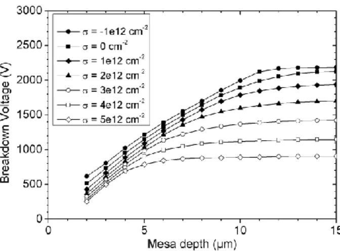
The wafers were then cut in one inch side square samples. PiN diodes were fabricated on samples of each type. In order to maintain a low stacking fault density, an ion-implantation-free process was used. A mesa termination was used both to define the diode anode periphery and to ensure an acceptable blocking capability. The influence of the mesa depth on the breakdown voltage has been studied by finite element method (Fig. 3), The ionization rates coefficients extracted by Konstantinov et al [5] were used in Sentaurus TCAD software. The ideal breakdown voltage, i.e. for a perfect planar junction, for such an N- layer is approximately 2200 V, as calculated by 1D simulation. It was decided to use an 8 µm deep mesa, which should result in a 1650 V breakdown voltage, considering a surface charge density of 0 cm-2.
The 8 µm deep mesa has been etched with SF6/O2 chemistry in a Reactive Ion Etching
equipment at 250 W, 60 mTorr and using Ni masks [6]. A Ni-based cathode ohmic contact of ~200 nm was formed on the whole n-type back side of the substrate. The ohmic contact on the p-Figure 1. Schematic cross-view of the
fabricated PiN diodes
Figure 3. Simulated breakdown voltage of PiN diodes as a function of the mesa etch depth and the surface charge density
Figure 2. Optical image of the wafer surface for nominally on-axis substrate.
type anode was realized by selective evaporation of Ni, Ti and Al layers with a ~300 nm total thickness [7]. A post-metallization Rapid Thermal Annealing (RTA) was performed at 900 °C for the cathode contact and at 800 °C for the anode contact. Right after an Ar etching, in order to avoid the formation of insulating interlayers, a 1.5µm thick Al layer was finally patterned on the anode contacts.
A comparison of the electrical behavior of PiN diodes fabricated on off-cut and on-axis grown epilayers has been drawn to study the influence of the growth processes. Direct electrical characterizations were performed using an agilent B1505 power curve tracer. The diodes reverse characteristics were measured by means of a 20 kV high-voltage probe in a vacuum chamber at ISL. Characterizations were done below 10-4 mbar ensuring a sufficient insulation.
Results and discussion
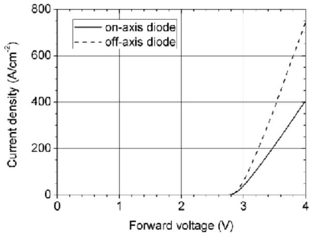
Figure 4 shows typical direct IV characteristics of diodes with the same surface area which were fabricated on the two different samples. The on-axis wafers give rise to slightly more resistive diodes than the off-axis wafers. This is due to the low doping concentration of the on-axis growth substrates which was typically in the mid 1017 cm-3. This value is one order of magnitude less than the doping concentration of the off-axis substrate.
0 100 200 300 400 500 600 700 0 2 4 6 8 10 0.0 1.6 3.2 4.8 6.3 7.9 R e v e rs e c u rr e n t d e n s it y ( m A /c m -2 ) R e v e rs e c u rr e n t (µ A ) Reverse voltage (V) on-axis diode off-axis diode
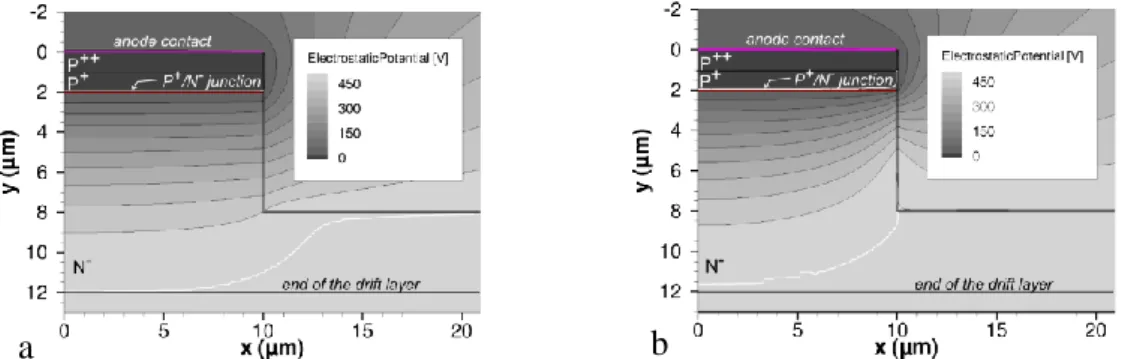
The reverse characterization revealed substantial disparity. Many diodes fabricated on the on-axis wafers present high leakage currents. It is assumed that this is due to the high surface roughness, which affects both the mesa thickness control and the N-/P- junction evenness. Nevertheless, some diodes sustain 600 V, which is comparable with the off-axis diodes (Fig. 5) and, to our knowledge, a record for such a wafer orientation. Unfortunately this result, though promising, is lower than what was anticipated by simulation. This could be explained by surface charges created during the mesa etching or the lack of a proper passivation layer. As shown on Fig. 3, the presence of a positive surface charge reduces the breakdown voltage. Fig. 6 shows the repartition of the equipotentials in a PIN mesa structure as calculated by simulations. As can be seen on Fig. 6b, when a positive surface charge is present, equipotential lines are more concentrated close to the mesa edge. This induces a higher electric field, which leads to a smaller breakdown voltage (see Fig. 3).
Figure 4. Comparison of the direct IV characteristic of 12×10-4 cm2 PIN diodes fabricated using the on-axis and off-axis wafers
Figure 5. Typical reverse IV characteristics of the PIN diodes fabricated on the on-axis and off-axis wafers
Conclusion
A N-/P+/P++ epilayer structure has been grown using an on-axis wafer. Mesa terminated PiN diodes were fabricated. Reverse current lower than 10 µA at 600 V was measured which is a very good result for such a substrate orientation. The same kind of devices was fabricated using epilayers grown on off-cut substrates for comparison, giving rise to breakdown voltage in the same range. Higher breakdown voltage could certainly be obtained thanks to a better control of the SiC RIE etching process and the use of a passivation layer.
Acknowledgement
The authors want to thank the Agence Nationale pour la Recherche, ANR, for its financial support in the framework of the Very High Voltage Devices SiC project (VHVD-SiC).
References
[1] C. Raynaud, D. Tournier, H. Morel, and D. Planson, Diam. Rel. Mat. Vol. 19 (2010), pp. 1-6 [2] J. P. Bergmann, H. Lendenmann, P. Å. Nilsson, U. Lindefelt, and P. Skytt: Mater. Sci. Forum
Vol.353-356 (2001), pp. 299-302
[3] J. Hassan, J. P. Bergman, A. Henry, and E. Janzen, J. Crystal Growth Vol. 310 (2008), pp. 4430-4437
[4] J. Hassan, J. P. Bergman, A. Henry, and E. Janzen, J. Crystal Growth Vol. 310 (2008), pp. 4424-4429
[5] A. O. Konstantinov, Q. Wahab, N. Nordell, and U. Lindefelt, Appl. Phys. Lett. Vol. 71 (1997), pp. 90-92
[6] F. Simescu, D. Coiffard, M. Lazar, P. Brosselard, and D. Planson, J. Optoelectron. Adv. Mater. Vol. 12 (2010), pp. 766-769
[7] F. Laariedh, M. Lazar, P. Cremillieu, J.-L. Leclercq and D. Planson, HeteroSiC-WASMPE’11 Conference, Tours, France (2011)
Figure 6. Simulated equipotentials in a mesa PiN diode N- layer at 500 V reverse bias depending on the surface charge density. a) for a 0 cm-2 charge density b) for a 5×1012 cm-2 charge density