Bubble Dynamics on Structured Surface in
Microchannel
by Siyu Chen
Submitted to the Department of Mechanical Engineering in Partial Fulfillment of the Requirements for the Degree of Master of Science in Mechanical Engineering
at the
Massachusetts Institute of Technology June 2013
@ 2013 Massachusetts Institute of Technology All rights reserved.
Signature of Author:
Vt
'- V'-ARCHTtV
MASSACHUSETTS INSTtftE OF TECHNOLOGYJUN 2 5 293
UBRARIES
Department of Mechanical Engineering May 10, 2013
A Certified by:
Evelyn N. Wang Associate Professor of Mechanical Engineering Thesis Supervisor A 0-t.0
Accepted by:
David E. Hardt Chairman, Department Committee on Graduate Theses
Bubble Dynamics on Structured Surface in
Microchannel
By
Siyu Chen
Submitted to the Department of Mechanical Engineering on May 10, 2013, in Partial Fulfillment of the Requirements for the
Degree of Master of Science in Mechanical Engineering
Abstract
Surface enhancement is a potential way to improve the performance of flow boiling in microchannels, which is considered to be one of the most promising cooling methods to solve thermal management challenges faced by future semiconductor products. Considerable research has been done on examining the functions of engineered surfaces. However, the mechanism of how these surfaces improve the flow boiling performance is still unclear.
In this thesis, bubble dynamics on micropillar array surfaces were studied. A surface energy based model is presented to predict the bubble morphology on pillar array surfaces. The results showed that bubbles tend to stay on top surfaces of pillars at solid fractions greater than 0.162, keeping liquid films underneath the bubbles. On the other hand, on surfaces at solid fraction less than 0.162, bubbles tend to propagate within the pillar unit cells.
A flow loop with good degassing and a fluid temperature control system was designed and built for various flow boiling experiments. Five different types of silicon micropillar array surfaces were fabricated. Moreover a setup for observing bubble dynamics in microchannels under flow boiling conditions was developed. Experiments were performed to investigate the bubble dynamics on silicon micropillar array surfaces. Bubble departure modes were observed. The bubble departure size of direct departing mode was found to be independent with flow rate while departure size of sliding mode decreased with increasing of the flow rate. Three potential methods to create single nucleation sites for improved studies of bubble dynamics were also presented in this thesis.
An experimental setup to investigate behavior of a single bubbles created by air injection on micropillar array was presented. Single 10-30 pm injection holes were fabricated on micropillar array surfaces by laser cutter. The experimental results show that structured surfaces have higher bubble departure sizes than that for a plain surface. The surfaces with solid fractions greater than 0.162 had larger departure sizes than that of surfaces with solid fractions smaller than 0.162 at mass flow rates above 250 kg/m 2s while departure sizes of the
higher solid fraction surfaces become smaller than that of lower solid fraction surfaces when flow rates decreased below 200 kg/m 2s. The similarity between the departure sizes obtained by
could provide useful information on understanding the vapor bubble departure behavior on micropillar array surfaces. Silicon micropillar array surfaces may have larger bubble departure sizes than plain surfaces, however, the surfaces with solid fractions greater than 0.162 are suggested for boiling due the a large amount of liquid thin films may create for higher heat transfer rates.
Thesis Supervisor: Evelyn N. Wang
Table of Contents
Abstract 2 Table of Contents 5 List of Figures 7 List of Tables 9 1. Introduction 11 1.1 Motivation 11 1.2 Backgrounds 111.3 Objective and Outline 18
2. Bubble Morphology on Structured Surface 19
2.1 Modeling 19
2.2 Chapter Summary 30
3. Flow Boiling Experimental Test Setup 31
3.1 Flow loop 31
3.2 Degassing Tank and Degassing Procedure 33
3.3 Inlet Water Temperature Control 37
4. Bubble Dynamics in a Microchannel under Flow Boiling Conditions 39
4.1 Test Sample: Silicon Micropillar Array Surfaces 39
4.2 Test Fixture 42
4.3 Experiment Procedure 44
4.4 Results and Discussion 44
4.5 Discussions of Advantages of Micropillar Array Surfaces 51
4.3 Chapter Summary 54
5. Bubble Departure on Silicon Micropillar Arrays Surface by Air Injection 55
5.1 Test Sample 55
5.2 Test Fixture 56
5.3 Experiment Procedure 58
5.5 Chapter Summary 65
6. Conclusions and Future Work 67
6.1 Recommendation for Future Work 68
7. Bibliography 69
Appendix 71
Appendix A Design of the Degassing Tank (unit: inch) 71 Appendix B Design of the Test Fixture for Flow Boiling in a Microchannel (unit: inch) 72
List of Figures
Figure 1-1: Figure 1-1 SEM images of microchannels with cavities. Kosar et al., Suppression
of Boiling Flow Oscillations in Parallel Microchannels by Inlet Restrictors, Journal of Heat
Transfer, 2006. (a) Nonconnected reentrant cavity microchannel (b) Interconnected reentrant
cavity microchannel. 16
Figure 2-1: Figure 2-1 Schematic showing (a) Cross section view of bubble nucleation at bottom of the pillars with an initial height of h' (b) Top view of the bubble nucleation at bottom of the pillars within a unit cell formed by four pillars; where d is the diameter of pillar and I is
the edge to edge pillar spacing. 20
Figure 2-2: The values of AE* at h' = h for silicon pillar array surface with various solid fraction and roughness. Higher solid fraction surfaces have lower AE* values and higher
roughness surfaces have higher AE* values. 22
Figure 2-3: Figure 2-3 Schematic showing (a) Cross section view of bubble potential growing
direction after filling the unit cell (b) Top view of bubble potential growing direction after filling the unit cell; where d is the diameter of pillar and I is the edge to edge pillar spacing. 24
Figure 2-4: The values of AE* for silicon pillars with various solid fraction and roughness. Higher solid fraction surfaces have lower AE* values and higher roughness surfaces have higher
AE* values. 25
Figure 2-5: Schematic showing (a) bubble grows downwards after reaching the corner of the
pillar (b) bubble grows with interface pinned at corner of the pillar; where d is the diameter of
pillar and I is the edge to edge pillar spacing. 26
Figure 2-6: Schematic showing (a) cross section view of bubble nucleates on top of pillars (b)
Top view of bubble nucleates on top of pillars and stay on four unit cells; where d is diameter of pillars, I is the pillar spacing, h is the height of the bubble and r is the radius of the bubble. 27 Figure 2-7: Values of AEt* for silicon pillar array surfaces with various solid fraction and
roughness in terms of bubble radius. 29
Figure 3-1: Schematic drawing of flow boiling loop. [1] Peristaltic pump [2] Flow meter [3, 6,
9, 11, 14] Thermal couple probes [4, 8, 10, 15] Vacuum valves [5] Degassing tank [7] Absolute
pressure sensor [12] Test fixture [13] Differential pressure sensor [16] Pre-heater [17]
Post-heater [18] Condenser 31
Figure 3-2: Flow boiling experimental setup 32
Figure 3-3: Design of the degassing tank 34
Figure 3-4: Heating control diagram of degassing tank 35
Figure 3-5: Comparison between tank pressure and water saturation temperature in terms
of temperature 36
Figure 3-6: Microchannel inlet water temperature variation 38
Figure 4-1: SEM images for the silicon micropillar array surfaces. (a) 5 pm diameter and 15 Im spacing; (b) 5 im diameter and 5 pm spacing (c) 10 prm diameter and 10 pm spacing (d) 10
lam diameter and 5 im spacing 40
Figure 4-2: Fabrication procedure of silicon micropillar array surface 41
Figure 4-4: Design of the fixture 43 Figure 4-5: Picture of the assembled flow boiling fixture and a schematic drawing for the
Pogo pin block. 44
Figure 4-6: Bubble growth and sliding process on 5 im diameter, 5 im spacing micropillar array surface. Channel dimension: 0.65 mm in height and 5 mm in width, Flow rate: 307.3 kg/m 2s, heat flux: 7.9 W/cm2.
45 Figure 4-7: (a) Bubble growth and direct departing process on plain surface. Flow rate: 307.7kg/m 2s; Heat flux: 7.9W/cm2
. (b) Schematic diagram of estimated effective area the
pressure acts on to cause bubble departure from the surface. 46 Figure 4-8: Bubble departure process due to the bubble interactions(a) Two bubbles merged and departed from surface (b) One bubble merged with a departed bubble and depart 47 Figure 4-9: Bubble departure process on plain surface due to the bubble oscillation. Flow
rate Flow rate: 307.3kg/m2s, heat flux: 7.9W/cm2 48
Figure 4-10: Departure radius in terms of mass flow rate under flow boiling condition.
Channel dimensions: 0.65mm in height and 5mm in width. 49 Figure 4-11: 10 im wide, 10 im deep hole created by FIB on 5 im diameter, 15 pm spacing
micropillar array surface. 51
Figure 4-12: Bubble regrowth process on plain surface and structured surface. (a) The bubble retouched the heat surface and grew into a slug on plain surface. (b) The bubble retouched the heated surface and experienced a slower regrowth process on a 5 Im diameter, 5 pm spacing
silicon pillar array surface. 53
Figure 5-1: Microscope images of laser holes on micropillar array surfaces. (a) 5 lIm
diameter and 10 pm spacing pillar arrays (b) 10 pm diameter and 10 pm spacing pillar arrays 56 Figure 5-2: Design of the fixture for bubble dynamics observation by air injection 56 Figure 5-3: Assembled test fixture for bubble dynamics observation by air injection 57 Figure 5-4: Bubble growth and departure process on 10 pm diameter and 10 pm spacing pillar array silicon surface under flow rate of 153.8 kg/m 2s. 58
Figure 5-5: Frames of bubble departure on different structured surfaces and corresponding best fit circles under a flow rate of 128.6 kg/m 2s. (1) Plain surface (2) 5im diameter and 15pm spacing (3) 5pm diameter and 5pm spacing (4) 10pm diameter and 10pm spacing 60 Figure 5-6: Departure radii in terms of mass flow rate for different silicon micropillar array
surfaces and plain silicon surface 61
Figure 5-7: Liquid-vapor interface growing process on micropillar array surface with high
solid fraction. 63
Figure 5-8: Comparison of bubble departure radii on 5 pm diameter, 15 pm spacing pillar array surface between 1.3 mm and 0.65 mm high channels 64 Figure 5-9: Comparison of bubble departure radius between injection experiments and flow
List of Tables
Table 2.1: Geometry Factors P, 23
Chapter 1
Introduction
1.1 MotivationThermal management has become one of the critical limitations for the development of semiconductor products. For example, the high-concentration photovoltaic (HCPV) solar cells were developed in order to enhance the optoelectronic transition efficiency and reduce the cost of solar cell systems at the same time. However, the HCPV cells also generate significant amounts of heat during the solar energy to electrical energy conversion. So far, the highest conversion efficiency of HCPV solar cells is around 42%, which are developed by Boeing Spectrolab [1]. This means, about 60% concentrated solar radiation is converted into the form of heat. Under a typical concentration of 1500 suns, the generated heat flux can reach as high as 120 W/cm2. If this heat cannot be dissipated effectively, the cell temperature will
dynamically increase, which will lower the energy-conversion efficiency [2-3] and may even cause burn out of the device.
Computer integrated circuit (IC) technologies are also facing such thermal management challenges. According to a review article by Pop, the power densities of commercialized computer chips already reach 100 W/cm2 [4] and predicted by Krishnan et al., the power
density of semiconductor-microarchitecture can reach as high as 1000 W/cm2 in the near future
[5]. Under such extreme heat dissipation conditions, traditional air-cooling methods or single phase liquid cooling method can no longer sufficiently cool the devices. Therefore, developing a more efficient cooling method is very important to meet the thermal management
requirements for future semiconductor-devices. 1.2 Backgrounds
Flow boiling in microchannels is one of the most promising cooling methods for cooling the high energy-density devices such as solar cells and computer chips. The advantage of this cooling method is utilizing the high surface area to volume ratio of microchannel and high
to provide uniform cooling across the devices due to the steady temperature during the boiling process.
However, the actual performance of flow boiling in microchannel cooling is limited by the critical heat flux (CHF), which indicates the maximum heat that a device can dissipate through this cooling method. Heat generation beyond the CHF will cause rapid increase of device temperature and may even cause device burn out. Therefore, it is very important to obtain a complete CHF data set and fully understand the CHF mechanism before applying flow
boiling in practical applications.
Many research studies have been conducted to investigate CHF data for various
micrchannels in various flow conditions. Mukherjee et al. developed a pumpless loop system to cool the hot devices with FC-72 [6]. The loop system consists of two parallel vertical tubes and
relied on the fluid density difference between those two tubes to drive the fluid motion. The heated copper surfaces with micro-fin enhancement were integrated into one tube with dimensions of 21.3 x 21.3 cm2. The height of the microchannel varied from 0.13 mm to 12.32
mm. The CHF values reported ranged from 25.5 W/cm2 to 62 W/cm2. Their experimental results showed that the smaller microchannels have higher CHF value and it can be further enhanced
by micro-fin structures compared to a plain surface.
Qu et al. fabricated 21 parallel rectangle microchannel arrays on a 4.48 cm X 1.0 cm oxygen-free copper block [7]. Each microchannel had a width of 215 Im and a height of 821 pim. The deionized water was driven by a gear pump through the microchannel heat sink at various
mass flow rates from 86 to 368 kg/m 2s. The CHF data were measured at two difference water
inlet temperature conditions: 30 'C and 60 "C. The reported effective CHF data ranges from 107.64 to 216.76 W/cm2 and as expected, the CHF increased with increasing flow rate. They also observed the strong vapor backflow when heat flux approaches CHF and they claimed that this is caused by the amplification of the parallel channel instability near the CHF condition. They believed that vapor backflow was the main reason why they did not see much change in
CHF for different water inlet temperature because the backward vapor flow led to the loss of subcooling.
Wojtn et al. attempted to establish a more complete CHF data set for the saturated flow boiling of R-134 and R-245fa in single microchannels with inner diameters of 0.5 mm and 0.8 mm [8]. They have developed a flow boiling loop, which was able to control the flow rate, refrigerant saturation temperature, heated length and liquid subcooling. A series of
experiments were performed at different flow conditions that can be controlled by the loop. The reported CHF data for R-134a ranged from 12 W/cm2 to 60 W/cm2 and the CHF data for R-245fa was from 175 W/cm2 to 450 W/cm2. They found that the CHF was influenced by flow mass velocity, heated length, microchannel dimension and fluid property. However, no obvious influence of subcooling was found.
A great number of research studies have focused on CHF of flow boiling in
microchannels where numerous CHF data were reported for various working fluids and flow conditions. However, the acquired CHF data are still not close enough to heat dissipation
requirement for the future high power density devices, which is 1000 W/cm2. Therefore, many efforts examined factors that caused CHF and investigated methods to improve the CHF. One of the common conclusions is that flow instability plays an important role on CHF of flow boiling in microchannel.
Bergles et al. reviewed existing CHF experiements for flow boiling in microchannel and summarized two major flow instabilities that affect CHF [9]. One of the instabilities is upstream compressible volume. As proposed in the paper of Boure et al. [10], when there is a
compressible volume upstream of the heated section, significant pressure drop oscillations will occur, which may lead to CHF. The other type of instability is excursive instabilities Kuo et al.
further extended these types of instabilities by adding two models: rapid bubble expansion and CHF instability [11]. This phenomenon is much more common in microchannels because the nucleated vapor bubbles experienced much faster growth rates under extremely high heat fluxes in such small confined spaces. The growth rate could be fast enough to suppress the upstream flow and cause large pressure drop oscillations. Under such conditions, certain heated area could experience a shortage of liquid supply and cause significant increase of device temperature, which would lead to CHF.
Past research has proposed methods to suppress these instabilities by increasing the upstream pressure. The most common method to achieve this is adding inlet restriction. Kandlikar et al. experimentally studied the pressure drop elements (inlet restriction) on the flow instability of flow boiling in microchannel [12]. Six parallel microchannels with rectangular cross section were machined on a copper block. Each microchannel has a hydraulic diameter of 333 pm and a length of 63.5 mm. Two different inlet restrictions with the 51% and 4% area of the cross-sectional area were added at the inlet of each microchannel. They investigated the videos and pressure drop oscillation data recorded during the flow boiling experiment and compared the results to their previous work, they found that 51% inlet restriction partially stabilized the flow but could not completely eliminate flow reversal. In the case of 4% inlet restriction, flow instability was completely eliminated, but at the same time, a significantly larger pressure drop was required to drive the flow in the microchannel.
Kosar et al. fabricated five parallel microchannels on the silicon wafer by photolithography and deep reactive ion-etching (DRIE) [13]. The dimensions of the
microchannels are 200 pm in width and 264 pm in depth. 20 pm wide inlet restrictors with various lengths were incorporated at the inlet of each microchannel. They experimentally studied how inlet restrictors affected the flow boiling performance of water. Their results agreed with previous results that inlet restrictors could eliminate the vapor backwards flow and stabilize the boiling flow. They also successfully correlated the onset of unstable boiling (OUB) heat flux q0,b and the pressure drop multiplier M, which is defined in Eq. 1.1. They found that
OUB heat flux increased with increasing M, which indicated that with more flow restrictions at the inlet of microchannels, better boiling performance can be achieved.
M = APmicrocoanner+Porifice
A microchannel
Park et al. further studied the effects of inlet restrictors on CHF of flow boiling for three refrigerants: R134a, R236fa and R245fa [14]. Two microchannel heat sinks consisting each of 20 parallel rectangular microchannels were tested: one had microchannels with 467 p.m width and 405 pm depth, the other had microchannels with 199 pm width and 765 pm depth. 300 pm
circular orifices were used for 467 lim wide microchannels and a rectangular slit with 200 pim in height was used for 199 tm wide microchannel to stabilized boiling flow. They measured the boiling curve and CHF data at various flow rates. Their results indicated that orifices were able to initiate boiling in microchannel at lower heat flux due to the high pressure drop they create and CHF values were improved at high flow rate. However, little improvement was observed in lower flow rate. No explanation was provided for this phenomenon, the little improvement on CHF may be caused by the less pressure drop the orifices create at low flow rates.
Many studies have shown that inlet restrictors can stabilize boiling flows and improve flow boiling performance. However, it may consume additional power to maintain same mass flow rate through restrictors compare to that without restrictors. Implementing inlet restrictors may work for applications where power consumption is not the limitation to achieve better performance. However, it can possibly become an issue when considering the applications in aerospace, where power is not sufficient; or applications such as cooling of solar cells, where tradeoff between how much more power it gains from better cooling system and how much power is put in to run the cooling system is a major concern.
Surface modifications promise heat dissipation performance by mitigating flow
instabilities. Kandlikar reviewed existing models on nucleation criteria of the cavity size and put forward a statement that with suitable design of cavity size, the wall superheat that initiates the nucleation can be reduced, which leads to a lower vapor pressure inside the bubble [15]. Thus, the quick bubble expansion can be suppressed and the flow instability can be eliminated.
Kuo et al.'s experimental results well-supported Kandlikar's model incorporating the role of nucleation sites on flow boiling [16]. They used devices with five parallel, 10 mm long, 200 ptm wide and 253 pm deep microchannels, which were fabricated on silicon by
photolithography followed by reactive ion etching (RIE) and deep reactive ion etching (DRIE). Two different types of reentrant cavities were added to the side walls of each microchannel, as shown in Figure 1-1. One had a 7.5 im mouth and 25 pm inside diameter reentrant body.
Reentrant bodies were separated from each other. The other type of cavities has same dimension but with the interconnected reentrant bodies. They also had the plain wall for
comparison. The flow boiling experiments were running at different flow rates from 86-520 kg/m 2
s. Their results well-indicated that good cavities were able to reduced onset nucleation boiling (ONB) wall temperature as well as ONB heat flux. They also measured the local wall temperature for the post onset flow oscillation (OFO) boiling. Their results showed that the devices with cavities had longer stable boiling region in terms of heat flux, which means flow instability were suppressed. Because of the extended stable boiling region, the CHF therefore was increased about 15-33%. The maximum CHF value that obtained in their work was about
200W/cm2 at a flow rate of 520 kg/m2s. (a)
Figure 1-1 SEM images of microchannels with cavities. A. Kosar, C. Kuo and Y. Peles,
Suppression of Boiling Flow Oscillations in Parallel Microchannels by Inlet Restrictors, Journal of Heat Transfer, 2006. (a) Nonconnected reentrant cavity microchannel (b) Interconnected reentrant cavity microchannel.
Li et al. studied flow boiling performance in nanowire-coated microchannels [17]. In their work, in situ silicon nanowires incorporated inside the 20 mm long, 250 Im wide and 200 Ipm deep microchannel arrays. Boiling curves, local wall temperature and pressure drops through microchannels were measured at various flow rates from 119 to 571 kg/m 2s. Heat
transfer coefficients were also calculated based on the measurement data. It was found that nanowire-coated microchannels successfully reduced the ONB wall temperature and delayed the OFO. Significantly smaller fluctuations of pressure drop and wall temperatures were observed for silicon nanowire enhanced surface compared to plain surface. Improvement of Heat transfer coefficient was also observed. The improvement was attributed to the structures
of nanowires, which provided sufficient nucleation sites to lower the wall superheat of boiling and suppressed the flow instability.
While designing nucleation sites are important for the initial stage for bubble formation, it is also very important to investigate the bubble growth and departure behavior after bubble nucleation. If the nucleated bubbles are not being removed efficiently, the bubbles still could grow and block the channel, which eventually leads to the upstream compressible volume instabilities. Numerous studies have investigated bubble dynamics during flow boiling in microchannels. Lee et al., explored the bubble dynamics in both single and two parallel
trapezoid microchannels [18-19]. Each microchannel had a hydraulic diameter of 41.3 ptm and a length of 28 mm. They measured the sizes of signal bubble and bubble slug during their growing process and found a linear dependence of bubble size on time for the single bubble and an exponential dependence on time for the bubble slug. The higher growth rate of slugs could be explained by thin film evaporation, which was the dominating heat transfer mechanism during slug evolution. They also observed some unusual bubble grow processes, which could not be explained by existing theories. In their papers, the bubble departure sizes were measured as well. Their results showed that the departure size was governed by the surface tension and drag of bulk flow. It was also found that the traditional frequency and departure diameter relationship was not applicable in their microchannel studies.
Kuo et al, however, concluded that the products of frequency and departure diameter might still be constant for microchannels. They studied the bubble dynamics of flow boiling in five parallel microchannels with interconnected reentrant cavities on side walls (similar cavities were shown in Figure 1-1b) [20]. They measured the bubble departure diameters and
corresponding departure frequencies and found that the products of frequency and departure diameter kept constant, which was similar to the macroscale. The difference was that the value of these products in microchannel was an order of magnitude smaller.
Although considerable research has focused on bubble dynamics of flow boiling in microchannels, common conclusions have not been reached yet. On the other hand, few research studies have focus on the bubble dynamics on structured surfaces and the actual
mechanism of bubble growth and departure is still unclear. Therefore, it is necessary to conduct research on bubble dynamics on structure surface under flow boiling conditions, to explore how the bubble grow and departure on the structured surface and understand how structured surface improve the flow boiling performance.
1.3 Objective and Outline
The objective of this thesis is to study the bubble dynamics on structured surfaces, to investigate the role of structures in bubble growth and departure behaviors and to understand how structures affect flow boiling performance in microchannels. The outline of this thesis is shown below:
In Chapter 1, the motivation for studying flow boiling in microchannel and bubble dynamics on well-defined-structured surfaces is presented. A brief literature review was done to show the state of the art for flow boiling in microchannel.
In Chapter 2, a model based on surface energy analysis was developed to predict the bubble morphology for pillar array surfaces with different surface geometries.
In Chapter 3, the design and implementation of the experimental flow boiling loop was presented.
In Chapter 4, the flow boiling experiments to explore the bubble dynamics on
micropillar array silicon surfaces were conducted. A test setup to observe bubble dynamics in microchannels in a side view was demonstrated in this chapter.
In Chapter 5, the departure behaviors of single bubble created by air injection from backside of micropillar array silicon surface were studied. Experiments of observing the bubble departure process in a side view was presented.
In Chapter 6, the conclusions of this thesis and the potential future works were presented.
Chapter 2
Bubble Morphology on Structured Surface
When the channel size is reduced to the microscale, the surface tension plays a very important role on the bubble dynamics. It affects the bubble nucleation, growth and departure process. Surface tension also affects the bubble morphology on surfaces, which is usually shown as changing of the contact angles. When structured surfaces are introduced, the bubble
morphology becomes much more complicated. It is critical to understand the bubble morphology on different structures because it indicates how bubble interact with surfaces, which could influence the overall surface tension on the bubble, the heat transfer area and even the heat transfer mechanism. As a result, it affects the bubble departure and flow boiling performance. Therefore, as the first step, the bubble morphology is studied.
We used micropillar array surfaces for our studies for the following reasons: First, the micropillar array surfaces are well controlled that surface properties such as roughness and solid fraction can be obtained from the pillar diameter, height and spacing, which facilitates modeling efforts to provide insights into how different surface properties affect bubble dynamics in microchannels. Second, the standard procedures have been established for fabricating micropillar arrays on silicon material by photolithography and deep reactive ion etching (DRIE). This makes it easy to interface with the potential applications such as computer chips, which are usually made from silicon. The details of the micropillar arrays on silicon substrate will be discussed in section 4.1.
2.1 Modeling
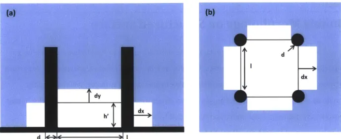
Firstly, the case that the bubble nucleates at the bottom of the pillar is studied. The bubble is simplified as a thin layer of vapor bubble that fills the bottom of a unit form by four pillars. The schematic drawing for this case is shown in Figure 2-1
d -lI| ;-
Figure 2-1 Schematic showing (a) Cross section view of bubble nucleation at bottom of the pillars with an initial height of h' (b) Top view of the bubble nucleation at bottom of the pillars within a unit cell formed by four pillars; where d is the diameter of pillar and I is the edge to edge pillar spacing.
Assume that the height of the original bubble in the unit cell is h'. Two potential growth directions can be seen in the figure: one is growing dy upwards and the other is growing dx laterally to fill the adjacent units. The surface energy change due to the bubble growing laterally in a length of dx can be calculated by the following equation:
A E = 4ysv Idx + 4yLv( 2h' + 1)dx - 4YSL 1dx . (Eqn 2.1)
The surface energy change due to the bubble growing upwards in a length of dy is:
AE = ysvirddy + YLv 4ldy - YsLddy; (Eqn 2.2) where Ysv, YLv and YsL are the surface energies of solid-vapor, liquid-vapor and solid-liquid interfaces. 1 is the spacing length between two pillar as shown in Figure 2-1. d is the
diameter of each pillar and h' is the height of the original bubble in the unit cell before it begin to grow. The range of h' from 0 to the height of pillar, is represented by h.
By comparing the energy changes in x and y direction, the preferable growth direction can be determined since the bubble always grows in the direction that has the
lower energy state. For easy comparison, a dimensionless energy term is defined as shown in Eq. 2.3:
E _Ey Ysvd + yLv 4I - YSLwd dy(
AEX 4Ysvl+4Lv(2h+1) -4 YSL dx
By applying the constant growth volume constraint, the relationship between dy
and dx can be obtained, as shown in Eq. 2.4:
[(I + d)2
- _d2] dy = 4h'ldx. (Eqn 2.4)
4
Substituting the Eq.2.4 into the Eq.2.3 and rearranging the equation, the AEg* can be expressed by the Eq. 2.5:
wd Ysv - YSL +41 h
AE* = LV - . (Eqn 2.5)
IYSV -YSL+ (2h' + 1) ( 2 d2
YLV
Noticing that (Ysv - YsL)/ YLV = cos Oy, where Oy is Young's contact angle, Eq. 2.5 can be further simplified, shown in Eq. 2.6:
7rdcosOy + 41 h'1
AE* rcs~ 4
'
. (Eqn 2.6)(lcos Oy + (2h' + 1)]
(1
+ d)2 - 'd2]For a hydrophilic surface, such as the silicon surface with oxide layer, the Young's contact angle will be less than 900. Thus a positive surface energy change will be obtained for a bubble growing in both x and y directions. Considering this fact, the criteria to
determine which direction the nucleated bubble prefers to grow can be achieved: if
AE* > 1, the bubble tends to grow horizontally; if AE* < 1, the bubble tends to grow
vertically.
When the bubble just starts growing inside the unit, which corresponding to h' -+ 0,
the value of AE* is infinitely small. This means the nucleated bubble will grow upwards to
fill the unit at the early stage. The AE* increases as the bubble grows inside a unit cell (h'
to check the value of AE* when h' = h to determine whether the vapor bubble will propagate into the adjacent unit or keep growing upwards until it fills the whole unit. The
AE* at h' = h for different micropillar array surfaces with various solid fraction and
roughness are plotted in Figure 2-2. For the silicon pillar array surface, the roughness r and solid fraction p are defined in terms of pillar diameterd, height h and spacing 1, which are shown in Eq. 2.7 and Eq. 2.8:
(1 + d)2 + irdh wdh
r= (+d) 2 =1+(l+d)2
ffd2
(1 + d)2
X
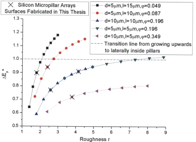
Silicon Micropillar Arrays Surfaces Fabricated in This Thesis1.2 1.1 1.0- 0.9- 0.8- 0.7-0.6 0.5 0< -4-(Eqn 2.7) (Eqn 2.8) 4- --A 4 4 I A 4 1 2 3 4 5 6 7 Roughness r 8 9
Figure 2-2: The values of AE! at h' = h for silicon pillar array surface with various solid fraction and roughness. Higher solid fraction surfaces have lower AE! values and higher
roughness surfaces have higher AE* values
+ d=5pm,l=1 5pim,<=0.049 -- d=5pm,=10p1m,<p=0.087
- d=10pm,l=10pm,<p=0.196
-v- d=5pm,l=5im,p=O.1 96
+ d=10pm,l=5pm,<p=0.349 --- Transition line from growing
upwards to laterally
From Figure 2-2, the characteristics of AE* plots are determined by solid fraction and roughness. Higher roughness will lead to higher AE[. On the other hand, a higher solid fraction will suppress this increase, which means the surface with high solid fraction can suppress the bubble propagating inside the micropillars. For surface that has a AE* value higher than 1, the bubble will start to grow laterally before it fills the whole unit. To determine how many units the bubble will fill before it reaches the top of pillars, the Eq. 2.6 is extended into a much more general form, as shown in Eq. 2.9:
AE* = PnAE* ; (Eqn 2.9)
where the geometry factors Pn is related to the number of units that have been filled by vapor, whose value is listed in Table 2.1. AE* compares the energy change for a bubble to grow upwards and the energy change for a bubble to grow laterally when it fills n pillar units. The smallest n that has AE* < 1 is the number of units that bubble will fill before it grows into the same height as the pillars.
Table 2.1 Geometry Factors Pn
No. of units 1 2 3 4 5 6
Pn 1 3/4 2/3 1/2 1/2 5/12
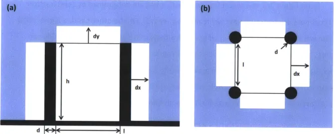
Next, the case that the water vapor fills the several units is considered. The purpose is to determine whether the water vapor prefers to grow upwards from the pillars or propagate laterally inside the pillars. The single unit is first considered here and then will be extended to a more general form. Figure 2-4 shows the schematic for this case. Following the similar energy analysis, the comparison between the energy change for a vapor bubble growing inside and outside the pillars is conducted.
d |C Pie :0||
Figure 2-3 Schematic showing (a) Cross section view of bubble potential growing
direction after filling the unit cell (b) Top view of bubble potential growing direction after filling the unit cell; where d is the diameter of pillar and I is the edge to edge pillar
spacing.
The energy change for a bubble growing inside the pillars in a distance of dx can be calculated by Eq. 2.10. And the energy change for bubble growing in a distance of dy can be calculated by Eq. 2.11:
LEinside = YsvIdx + YLv( 2h + l)dx - YSLldx
AEoutside = YLv(fd + 41)dy.
(Eqn 2.10) (Eqn 2.11)
We define a new dimensionless energy term by dividing AEoutside by AEinside to
determine the preferable growth direction. Young's equation and constant volume constraint are applied to simplify the equation and a final expression for this new dimensionless term is shown in Eq. 2.12:
_d + 41 hl
- [Icos y + (2h + 1)]
(l
+ d)2 -d2] (Eqn 2.12) If AE* > 1, the bubble tends to grow inside the pillars; if AE* < 1, the bubbletends to grow upwards. The AE* for surfaces with various roughness and solid fraction are plotted in Figure 2-4. Similar to the AE*, the AE* increases with increasing roughness and a
higher solid fraction can suppress this increasing trend, which indicates bubble prefers to grow upwards from the micropillars with a high solid fraction and low roughness. Surfaces with different pillar diameters and spacing but same solid fraction also follow the same trend for the AE* value.
X
Silicon Micropillar Arrays -w- d=5jam,l=15pm,p=0.049 Surfaces Fabricated in This Thesis + d=5[im,l=10pm,9=0.0871.3 -A-- d=10gm,l=10im,p=0.196
1.2 -v- d=5pm,l=5pm,p=0.1 96
4 d=10jim,l=5[Lm,e=0.349
1.1 --- Transition line from growing upwards
to laterally inside pillars
1.0 - --- - - - --- ---W 0.9-0.8 -4
0.7-
/~
0.6-4 0.5 1 2 3 4 5 6 7 8 9 Roughness rFigure 2-4: The values of AE* for silicon pillars with various solid fraction and roughness. Higher solid fraction surfaces have lower AE,* values and higher roughness surfaces have
higher AE* values
In a third case, we considered the bubble filling one unit cell and growing upwards from micropillars. It is reasonable to predict that the liquid-vapor interface will advance on top of pillar surface until it researches the corner, as shown in Figure 2-5. There are two potential ways for the bubble to grow further. One is that the liquid-vapor interface start to grow downwards and the other is the liquid-vapor interface is pinned at the corner. In
analysis. Assuming that the liquid-vapor interface grow down in a length of dy. The energy change due to this interface movement can be calculated by Eq. 2.13:
wd
AE = (Ysv -YSL) -dy -YLv dy.
2 (Eqn 2.13)
Dividing both sides by yLv(l + d)dy, a dimensionless term can be obtained and defined as AEy*. Replacing d and I by the solid fraction, a final expression can be obtained,
shown in Eq. 2.14:
AEY
My* =
E
=Lv - COS6yifr, + 2 - - 1. (Eqn 2.14) YLV(1 +d)dyFigure 2-5 Schematic showing (a) bubble grows downwards after reaching the corner of the pillar (b) bubble grows with interface pinned at corner of the pillar; where d is the diameter of pillar and I is the edge to edge pillar spacing.
If AEy* < 0, which means moving down the liquid-vapor interface, leading to a lower energy state, the vapor will soon cover the other side of the pillar and start to fill the next unit. A Wenzel bubble, which is defined as a bubble that fills the pillar unit cells, is much easier to form; If AEy *>0, the liquid-vapor interface will pin at the top corner until the interface reaches next pillar's top surface. In this case, a Cassie bubble, which is defined
as a bubble that stays on top of the pillars with a liquid layer underneath the bubble, is much easier to form. Therefore, a criterion to determine which type of bubble that is easier to form on the surface can be obtained. For the naturally oxidized silicon surface, the contact angle is approximately 40*, which results in a critical solid fraction of 0.162.
1 (p > Cassie Bubble JTcos2Oy + 4cos67 +-1 qp < 4 Wenzel Bubble fcos26y + 4cosOy +
-In a fourth case, the bubble nucleate on top of the pillar is considered. The process is simplified as the bubble first nucleates on the top of one pillar and starts to grow until it reaches the nearby pillars. Here, homogeneous growth is considered and the bubble will first covers four pillar unit cells as shown in Figure 2-6. After this, bubble can keep growing above the pillars or start to grow down to fill the pillar unit cells. Similar energy analysis is done to determine which way is preferable for the bubble to grow.
Qh
d I
Figure 2-6 Schematic showing (a) cross section view of bubble nucleates on top of pillars (b) Top view of bubble nucleates on top of pillars and stay on four unit cells; where d is diameter of pillars, I is the pillar spacing, h is the height of the bubble and r is the radius of the bubble.
The energy changes for a bubble growing outside the structure with radius and growing downwards in a length of dy are compared. The relationship between bubble radius r and bubble height h is shown in Eq. 2.15; the volume and surface area of the
bubble can be calculated as V = uh2(r
- ) and S = 2rrh. Base on this, simple
3
relationships between change in volume and change in surface area due to the change in radius can be calculated, as shown in Eq. 2.16 and Eq. 2.17:
dh r h = r + r2 _p 2, -= 1+ dr _rp2 dV dh dh - = Trh 2 + 2Trh d- - Trh2 -dr dr dr 1+d p = 22 dS dh d = 2h + 2 r -. dr dr (Eqn 2.15) (Eqn 2.16) (Eqn 2.17) Consider the bubble grows down into the pillar units. Assuming it grow down by a length of dy, then the change of volume equals to dV = (4(1 + d)2
- lTd 2)dy. This change
of volume should equal to the volume change for a bubble growing outside the pillars in Eq. 2.16. Thus the relationship between dr and dy can be obtained as shown in Eq. 2.18. The change of surface energies for a bubble growing outside structures and growing into the structures can be determined based on the area change of liquid-vapor interface, which are showed in Eq. 2.19 and Eq. 2.20:
dr 4(1
+
d)2 - Td 2h2+2rdr dr
(Eqn 2.18)
AEU = YLVdS = YLV (2Th + 2Tr r-) dr
) + dh
A Ea = (YsV -Yst)4lndd y + yLV 8ld y .
(Eqn 2.19)
(Eqn 2.20) In this thesis, we defined a new dimensionless energy term AEt* to determine whether a bubble grows outside structures or inside structures by dividing AEu by AEd,
shown in Eq. 2.21. If AEt* > 1, the bubble will grow into the structures; if AEt* < 1, then the bubble will grow outside structures.
i h dh
YLv(2Th + 27r) dr
(
h +Tr -g) dr(Ysv-YSL)41Tddy + YLv 81 dy 2iTdcos6y + 41 dy (Eqn 2.21)
4'C w 1.2- 1.0- 0.8- 0.6-0.4 - 0.2- 0.0-7 I . yA . t , e. A V 4 , V 10 0 I I 20 30 40 r (um) 50 60
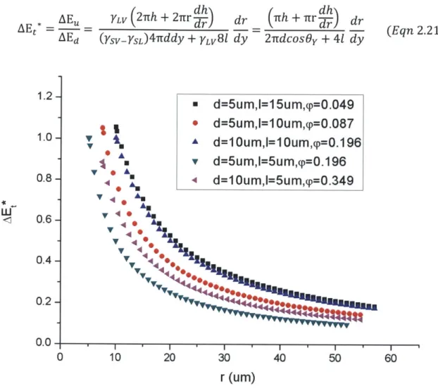
Figure 2-7 Values of AEt* for silicon pillar array surfaces with various solid fraction and roughness in terms of bubble radius.
Figure 2-7 shows the values AEt* for different pillar array surfaces. From the figure, the data points are all nearly lower than 1 except few points that have the values of radius very close to the spacing. These cases will not happen in practical scenarios because it
requires the bubble to grow larger than the distance to reach the nearby pillars. Thus it can be concluded that a bubble that grows on top of the pillars will never grow down to fill the pillar units. AEt = AE-A Eda = d=5um,I=15um,p=0.049 e d=5um,l=1Oum,p=0.087 A d=1Oum,1=1Oum,<p=O.196 v d=5um,l=5um,<p=0.196 4 d=1Oum,l=5um,<p=0.349
2.2 Chapter Summary
In this chapter, modeling work has been done to predict bubble morphology on micropillar array surface. By energy analysis, it is found that on high solid fraction surfaces, when a bubble nucleates at bottom of pillars, it tends to grow upwards to fill the pillar unit cell and starts to grow above the pillars; on the other hand, on low solid fraction surfaces, a bubble that nucleates at bottom of pillars will first propagate into several adjacent pillar unit cells before it start to grow above the pillars. It also has been found that the bubble will keep filling the pillar unit cells during its growth process on low solid fraction surface after it start growing above pillars, therefore a Wenzel bubble will form. On high solid fraction surfaces, the liquid-vapor interface will pin at top corner of the pillar and form a Cassie bubble. The critical solid fraction for silicon micropillar array surfaces to have a transition from Wenzel bubble preferable surface to Cassie bubble preferable surface has been found to be 0.162. The modeling work further showed that when a bubble nucleates on top of pillars, it will never grow down to fill the pillar unit cells.
Chapter 3
Flow Boiling Experimental Test Setup
To study the bubble dynamics in microchannel under flow boiling condition, a flow boiling loop is necessary to run various experiments. In this thesis, a flow loop was designed and built.
3.1 Flow loop
The schematic drawing of the built flow boiling loop is shown in Figure 3-1. As can be seen from the figure, the loop started with a peristaltic pump (L/S* Easy-Load® Il pump head, Masterflex*), which provided constant flow rate ranges from 0.36 - 1000 mL/min. A flow meter (FLR1000 ST, Omega) was connected right after the peristaltic pump to measure the flow rate of the loop. After the flow meter was the pre-heater. The pre-heater was a coil made of copper tube and wrapped with high-temperature heat cable, where the water was preheated to a state close to saturated state. A thermocouple probe was added after the pre-heater to measure the water temperature after the pre-heater. A self-designed degassing tank was located after the
pre-heater. The degassing tank was covered with several Kapton heaters controlled by an on/off controller. In the degassing tank, water was heated to a desired temperature and then pumped into the test fixture. More details on the degassing tank will be discussed in section 3.2. A high-temperature rope heater was wrapped on the copper tube between the degassing tank and the test fixture to prevent heat lost from natural convection. Different test fixtures for different experiments were placed after the rope heater wrapped tube and a differential
pressure sensor was mounted on the fixture to measure pressure drop across the microchannel. Two thermocouple probes were added on the inlet and the outlet of the test fixture to measure the inlet and outlet flow temperatures. After the test fixture was a condenser. The condenser was a long copper tube with a fan placed on top of it. The fan provided constant air flow to cool the water inside the copper tube. After cooled by the condenser, the water was pumped back to the peristaltic pump and started a new cycle.
The voltage signals of the pressure sensors and the flow meter are acquired by an NI data acquisition (DAQ) board (USB 6211, NI) and then transfer to a LabView program, where the signals are converted into the actual pressure and flow rate measurements. The
temperature signals from the thermocouple probes are collected by a digital thermocouple monitor (SR630, Stanford Research System) and then the collected temperature information is transferred to the Labview program through a GPIB cable. All the flow rate, pressure and temperature measurements were record by the Labview program every 1 second.
The test fixtures were placed on an inverted microscope (Eclipse Ti, Nikon), which was used to observe the bubble behaviors inside microchannel. The bubble dynamics was recorded by a high speed camera (Phantom v 7.1, Vision Research). The picture of complete flow boiling loop setup is shown in Figure 3-2.
To prevent contaminations, all components of the loop were cleaned by acetone, isopropyl alcohol (IPA) and Dl water before they were assembled into the loop. The whole loop was also flushed by DI water before each experiment to ensure the clean experimental
environment. 13 8 184 17 6 112 3 15 0 0 0 12 16
Figure 3-1 Schematic drawing of flow boiling loop. [1] Peristaltic pump [2] Flow meter [3, 6, 9, 11, 14] Thermal couple probes [4, 8, 10, 15] Vacuum valves [5] Degassing tank [7] Absolute
pressure sensor [12] Test fixture [13] Differential pressure sensor [16] Pre-heater [17] Post-heater [18] Condenser
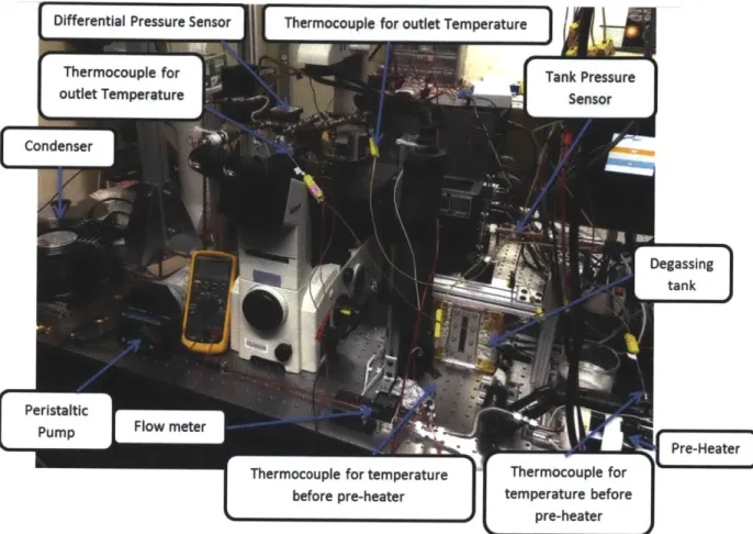
I
Differential Pressure Sensor Thermocouple for outlet Temperature=Condne
r
itltc
LPumptc
Figure 3-2 Flow boiling experimental setup 3.2 Degassing Tank and Degassing Procedure
Considerable amount of air may be either trapped inside the flow loop or dissolved in the deionized (DI) water, which will affect water nucleation and water vapor expansion inside
microchannel. In order to capture the pure water vapor bubble dynamics, a degassing procedure is necessary before the experiment.
Water degassing can be achieved by the degassing tank. The design of the degassing tank is shown in Figure 3-3. The degassing tank is a cubic tank made of stainless steel. One port is located on top of the tank, which is designed for pressure sensor. This port also allows air or water vapor to vent and release the pressure inside. Inlet and outlet ports are located at two
sides of the tank. A narrow rectangular window is implemented on the front side of the tank, which is used for observing the water level inside. The observing window is covered by a polycarbonate sheet with 0-ring sealing and was fixed on the tank by a stainless steel plate. A large window is opened at the bottom of the tank. This window is designed for cleaning
purpose and is covered by a stainless steel mounting with O-ring sealing. At the backside of the tank, a port is added, where a thermocouple is inserted to measure the liquid temperature inside. The details about dimensions of the degassing tank can found in Appendix A.
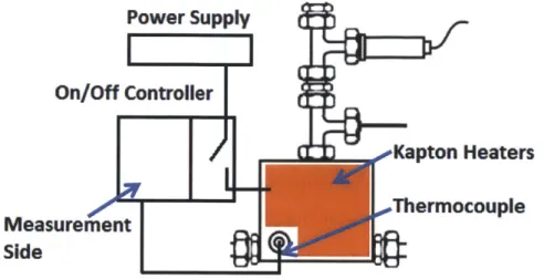
The tank is covered by several Kapton heaters, which are able to heat the water inside. These Kapton heaters are connected to an On/Off controller (CN7800, Omega), which is connected to a power supply. The thermocouple probe that measures the water temperature inside the tank is also connected to the On/Off controller. If the temperature measurement from the thermocouple probe is greater than the desired temperature, the controller will shut the power of the Kapton heaters. Otherwise, the Kapton heaters will keep heating the tank. By this way, the degassing tank can heat the water to a desired temperature. The schematic drawing of degassing tank and heating control wiring diagram is shown in Figure 3-4.
Observing Window
[
Port for pressure sensor and pressure releasing#Kapton Heaters
-Thermocouple
Figure 3-4 Heating control diagram of degassing tank
The following steps show the degassing procedure that was used in this thesis. (1) Heat the water inside the tank to 105 *C with valves 4,8 and 10 closed (valves'
location can be found in Figure 3-1).
(2) Open the valve 8 when pressure inside the tank increases to 140 kPa or stabilizes at more than 120 kPa.
(3) Close the valve 8 when the pressure inside the tank goes blow the 110 kPa and the Kapton heaters will start heating the water again.
(4) Repeat the step 2 and step 3 for 5 times.
By conducting the above procedure, the water inside the tank could be well degassed. The idea of this degassing procedure is to create large pressure difference between inside and outside degassing tank, so that the air inside tank will be drawn out of the tank when the top valve is opened. Therefore the air concentration in the tank will significantly decrease. According to the Henry's Law, which is shown in Eq. 3.1, the amount of dissolved air is proportional to the air concentration above water. Decreasing the air concentration can decrease the dissolved air in the water. When the air concentration becomes very low, the pressure inside the tank will be stabilized at the saturation pressure corresponding to the target heating temperature (here is 105 *C). Setting the heating temperature above 100 *C is to ensure a large enough pressure difference to push the air out even its concentration is very low:
p = kHc;
where p is partial pressure of air above water and c is concentration of air that dissolved in the water.
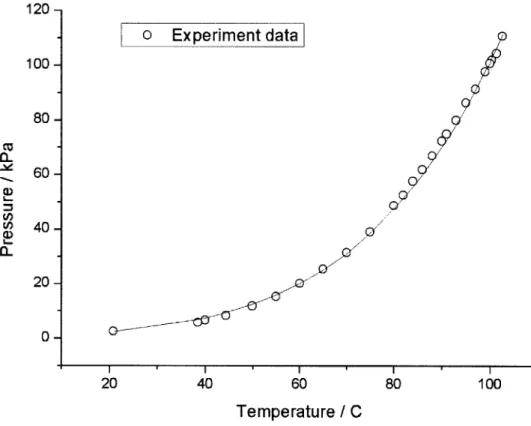
To examine whether the water is well degassed or not, tank pressure at various temperatures are measured. Figure 3-5 shows the measure tank pressure after degassing
procedure. From the figure, it can be seen that the tank pressure plot is well matched the saturation temperature of water, which indicates very good degassing is achieved.
0 Experiment data
l
9//
I' I I 40 60 Temperature / C 80Figure 3-5 Comparison between tank pressure and water saturation temperature in terms of temperature
In order to remove the air inside the loop, a vacuum pump is connected through valve 15. After water is degassed in the degassing tank, the pump is then turned on to remove the air in the rest of loop. Because of the relatively high pressure inside tank, when valve 4 and 10 are
120 - 100-80 -60 -40 -20 - 0-CU VI) 20 100 Eqn 3.1
opened, the degassed water will automatically fill the whole loop. After this, the flow loop is ready for running various experiments.
3.3 Inlet Water Temperature Control
In flow boiling experiments, it is very important to have a good inlet temperature control system for various experiments. It is even more crucial for bubble dynamic experiments because it is necessary to heat the water close to a saturation state before it enters into the microchannel, so that it will be much easier to generate bubbles inside the microchannel. In the current flow loop, controlling of the inlet water temperature was achieved by a pre-heater [16], a degassing tank [5], and a post-heater [17], as shown in Figure 3-1. The water was first heated
by the pre-heater to about 90*C. Then the water entered the degassing tank, where it was further heated to a target temperature. This was done by placing a thermocouple probe at the outlet port of the degassing tank and using the measured values of the outlet water
temperature as an input signal for the On/Off controller. When the exit water temperature was below the target temperature, the controller turned on the power of the Kapton heaters to heat the water inside degassing tank until the exit water temperature reached the target temperature. The water coming out of the tank was transported through a vertical section of
pipe before entering the microchannel. A post-heater was installed on the vertical pipe to compensate for any heat lost during the transportation. The temperature of the inlet water into the microchannel was monitored throughout the experiments.
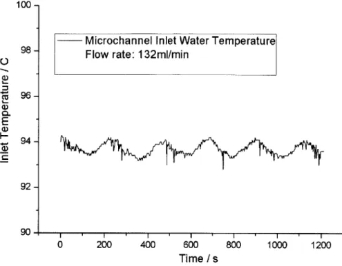
The inlet temperature variation during 20 minutes duration at a flow rate of 132 mL/min is shown in Figure 3-6. As can be seen from the figure, the inlet temperature varied no more than +/-1"C. This temperature oscillation was caused by the on/off control method. However, considering that the operating temperature is around 100*C, and that the period of
temperature oscillation was long compared to the bubble nucleation period, this inlet temperature variation was acceptable for boiling experiments.
Microchannel Inlet Water Temperature Flow rate: 132ml/min
I I I I
0 200 400 600
Time / s
800 1000 1200
Figure 3-6 Microchannel inlet water temperature variation
3.4 Chapter Summary
In this chapter, a flow loop for various experiments is presented. The loop can provide very good degassing work and fluid temperature control. The whole loop setup was built around an optical microscope, which allows people to observe and record images for experiments. 100 -98 -0 U) CU U) 0. E U) H U) C 96- 94- 92-
90-Chapter 4
Bubble Dynamics in a Microchannel under Flow Boiling
Conditions
In order to understand the bubble dynamics on structured surfaces in a microchannel under flow boiling conditions, several experiments are conducted. In this chapter, an
experimental setup that allows for observation of the bubble dynamics in a microchannel in a side view and the preliminary results are presented.
4.1 Test Samples: Silicon Micropillar Array Surfaces
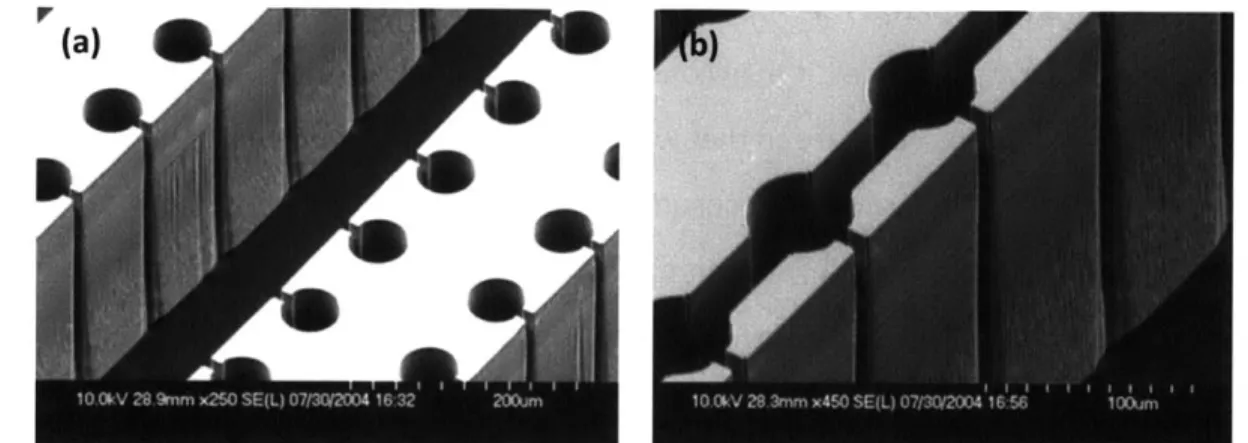
The structure surfaces studied in this thesis were silicon micropillar array surfaces. Figure 4-1 shows the SEM pictures of the micropillar array surfaces. Pillars of five different sizes were fabricated. The diameters of the pillars were 5 im and 10 ptm and the spacing (edge to edge) were from 5 pm to 15 prm. All pillars had a height of 20 pm. Table 4.1 shows the details of
pillar dimensions and corresponding surface properties. The pillar dimensions were designed to meet the imbibition condition [21], which is a criterion for water to completely wet the surface, as shown in Eq. 4.1:
y < 6c with cosc = Eqn 4.1
r
-where Oy is the equilibrium contact angle, T is the solid fraction and r is the roughness. Table 4.1 Dimensions of silicon micropillar array surfaces
Device # Diameter(pm) Spacing(pm) Height(pm) r p Oc
1 5 15 20 1.785 0.049 56.78
2 5 10 20 2.396 0.087 66.71
3 10 10 20 2.571 0.196 70.21
4 10 5 20 3.793 0.349 79.11
Figure 4-2 shows the details of the fabrication procedure. The procedure started with a 6 inch silicon wafer with a 300nm silicon dioxide layer on the surface. A 2 rn thick layer of OCG 825 positive photoresist was first coated onto the silicon surface by spin coating. Then
photolithography was used to produce the pillar pattern on the photoresist layer. Next, the silicon wafer underwent a Reactive-ion etching (RIE) to etch through the silicon dioxide layer, which transferred the pillar pattern from the photoresist layer to the silicon dioxide layer. After
RIE, the Deep Reactive-Ion Etching (DRIE) was processed to etch the 20 rn high pillars. In this step, the silicon dioxide layer works as a mask, which was good for etching high aspect-ratio structures. After DRIE was the piranha cleaning to remove the photoresist and the wafer was further cleaned by acetone, IPA and DI water. Lastly, the wafers were cut by dice saw into
33mm x 21mm pieces for experiments.
Figure 4-1 SEM images for the silicon micropillar array surfaces. (a) 5 pm diameter and 15 pm
spacing; (b) 5 pm diameter and 5 pm spacing (c) 10 pm diameter and 10 pm spacing (d) 10 pm diameter and 5 pm spacing
(1) Photoresist Coating: Spin Coating
(3) Reactive-Ion Etching (4) Deep Reactive-Ion Etching
(5) Piranha Clean
Photoresist Silicon Dioxide Silicon
Figure 4-2 Fabrication procedure of silicon micropillar array surface
In flow boiling experiments, a heater is necessary for providing heat flux from the backside of the sample for bubble nucleation. In this thesis, a 6.35 mm wide and 25.4 mm long Kapton heater was used. It bonded to the silicon sample by thermally conductive epoxy. A layer of non-conductive epoxy was then coated on top of the Kapton heater to prevent water from directly contacting the heater, and therefore no bubble would generate at the backside of the heater. Then the silicon sample was bonded to a Teflon block by the same non-conductive epoxy. The epoxy coating cured after 24 hours at 850C. Then the sample along with the Teflon
block was placed into the fixture for experiments. Figure 4-3 shows the layout of the silicon sample with the Kapton heater.
Silicon Sample with - - Kapton Heater
Structured Surface
Teflon Block Heater Wire and Contact Pad
Non-Conductive
Epoxy
Figure 4-3 Layout of structured silicon sample with Kapton heater 4.2 Test Fixture
A testing fixture was designed for the flow boiling experiment. The design of the flow
boiling fixture is shown in Figure 4-4. The fixture consisted of an inlet/outlet port, sample sink where the test sample would be installed and a Pogo pin slot for wire connection of the Kapton heater at backside of the silicon sample. A sandwich style method was used to form the channel
by two structured silicon samples and multiply silicon samples with smaller height in between
as the spacers. Thus the channel dimension was determined by the number of spacers used. Samples were then placed into the sample sink in the fixture with 2 Teflon blocks, which were used to fix the samples tightly in the fixture. On top of the fixture, a steel clamping plate was used to seal the channel with a Lexan glass providing optical access, which allowed observation of bubble dynamics in the microchannel in a side view. The details of dimension of this test fixture can be found in Appendix B.
![Figure 3-1 Schematic drawing of flow boiling loop. [1] Peristaltic pump [2] Flow meter [3, 6, 9, 11, 14] Thermal couple probes [4, 8, 10, 15] Vacuum valves [5] Degassing tank [7] Absolute](https://thumb-eu.123doks.com/thumbv2/123doknet/14186411.477219/32.918.118.777.648.987/figure-schematic-drawing-boiling-peristaltic-thermal-degassing-absolute.webp)