BlueFlash: A Reconfigurable Flash Controller for
BlueDBM
by
Ming Gang Liu
B.A.Sc., University of Toronto (2012)
Submitted to the Department of Electrical Engineering and Computer
Science
in partial fulfillment of the requirements for the degree of
Master of Science in Electrical Engineering and Computer Science
at the
MASSACHUSETTS INSTITUTE OF TECHNOLOGY
September 2014
c
○ Massachusetts Institute of Technology 2014. All rights reserved.
Author . . . .
Department of Electrical Engineering and Computer Science
August 29, 2014
Certified by . . . .
Arvind
Professor
Thesis Supervisor
Accepted by . . . .
Leslie A. Kolodziejski
Chairman, Department Committee on Graduate Theses
BlueFlash: A Reconfigurable Flash Controller for BlueDBM
by
Ming Gang Liu
Submitted to the Department of Electrical Engineering and Computer Science on August 29, 2014, in partial fulfillment of the
requirements for the degree of
Master of Science in Electrical Engineering and Computer Science
Abstract
NAND flash has risen to become a popular storage medium in recent years due to its significant bandwidth, access latency and power advantages over traditional hard disks. However, in modern Big Data systems, simply replacing disks with flash does not yield proportional performance gains. This is because of bottlenecks in various levels of the system stack: I/O interface, network, file system and processor. Intro-duced in 2012, BlueDBM is a novel Big Data flash storage platform that includes a dedicated low latency sideband storage network between flash controllers, reconfig-urable fabric for implementing in-store hardware accelerators and a flash-aware file system. While results are promising, the original BlueDBM platform used old flash boards that were merely 16GB in capacity running at 80MB/s. This work presents BlueFlash, a revamped and improved storage device for the BlueDBM platform. We present the design of a new 0.5TB flash board, a new ONFI-compliant FPGA-based flash controller with ECC and we explore the characteristics of the flash board. We demonstrate that BlueFlash scales well with multiple buses and multiple chips per bus, reaching 1.2GB/s (75% of theoretical max) read and 1.0GB/s (91% theoretical max) write bandwidth while consuming only 6W of power.
Thesis Supervisor: Arvind Title: Professor
Acknowledgments
I would like to thank my advisor, Prof. Arvind, for his support and guidance that made this large-scale project possible. I would also like thank Dr. Jamey Hicks, Dr. Larry Stewart, Marco Wu from Quanta and Rick Ballantyne from Xilinx for their efforts and contributions to the development of the flash board. Finally, I would like to acknowledge everyone involved with BlueDBM, Sang-Woo Jun, Dr. Sungjin Lee and Shuotao Xu for their continual work on the platform, as well as Dr. Abhinav Agarwal for his assistance with ECC.
Contents
1 Introduction 13
1.1 Flash in Big Data Systems . . . 13
1.2 Bottlenecks in Flash Storage Systems . . . 14
1.3 BlueDBM: A Hardware Accelerated Flash Storage Platform for Big Data 16 1.3.1 BlueDBM Architecture . . . 16
1.3.2 BlueDBM Stack . . . 16
1.4 Improving the BlueDBM Platform Hardware . . . 19
1.5 BlueFlash: A 0.5TB Flash Board and Controller . . . 19
2 BlueFlash Board Design 23 2.1 Flash Board Organization and Component Choices . . . 23
3 BlueFlash Controller Design and Implementation 29 3.1 Controller Interface . . . 29
3.2 Micron MLC NAND Chips . . . 31
3.3 Architecture Overview . . . 32
3.4 NAND I/O Primitives . . . 33
3.5 Read Capture Calibration . . . 35
3.6 ONFI-compliant PHY . . . 37
3.7 Bus Controller and Scoreboard . . . 37
3.8 ECC Encoder and Decoder . . . 39
3.9 Flash Controller . . . 41
4 Verification and Evaluation 43
4.1 Development Tools . . . 43
4.2 Verification and Test Setup . . . 43
4.3 Resource Usage . . . 44
4.4 NAND Page Bit Errors . . . 45
4.5 Access Latency . . . 45
4.5.1 Read Latency . . . 45
4.5.2 Write Latency . . . 46
4.6 Bandwidth and Scaling . . . 47
4.6.1 Chips Per Bus Scaling . . . 47
4.6.2 Number of Buses Scaling . . . 48
4.7 Power Consumption . . . 49
5 Related Works 51
List of Figures
1-1 BlueDBM Architecture . . . 17
1-2 BlueDBM Hardware Software Stack . . . 18
1-3 BlueFlash in the BlueDBM Stack . . . 21
2-1 FMC Flash Board Attached to Carrier Board . . . 24
2-2 NAND Chip Connections on a Bus . . . 25
2-3 Flash Board Architecture . . . 27
2-4 BlueFlash Board Hardware and Layout . . . 28
3-1 Micron MLC NAND Package . . . 32
3-2 Flash controller architecture . . . 33
3-3 Synchronous DDR Data (DQ) and Strobe (DQS) . . . 34
3-4 Controller NAND I/O Primitives . . . 35
3-5 PHY Data Output Cycle . . . 38
3-6 Interleaving of NAND flash commands . . . 39
3-7 Scoreboard architecture . . . 40
3-8 Reed Solomon encoder architecture (shrunken version with 4 word blocks) 41 4-1 Bit Errors Per Page Distribution (% Occurrence) . . . 46
4-2 Read Access Latency Breakdown . . . 46
4-3 Write Access Latency Breakdown . . . 47
4-4 Bandwidth Scaling by Number of Chips Per Bus . . . 48
4-5 Bandwidth Scaling by Number of Buses . . . 49
List of Tables
2.1 NAND arrangements for a 512GB flash card . . . 25 2.2 FMC Flash Board Specifications . . . 26 4.1 Resource Usage of Key Modules . . . 44
Chapter 1
Introduction
NAND flash has risen to become a ubiquitous storage medium in recent years. Com-pared to its hard disk counterpart, flash provides orders of magnitude better perfor-mance in both sequential and random workloads, as well as 100x lower access latency at 4x lower power[27]. Furthermore, flash density has scaled directly with transistor size and the ability to store multiple bits per cell, quickly reaching the low cost level of hard drives at comparable capacities. Raw bandwidth has also increased steadily with higher clocked interfaces and chips.
1.1
Flash in Big Data Systems
Because of its significant performance and cost benefits, flash based storage has found its way into modern Big Data systems. Big Data applications are characterized by their large size, high transactional volume, and/or complex analytical queries. Statistical analysis on large quantities of social media data (Twitter or Facebook) to identify consumer trends is one such example. The hardware system used today to perform such analytics typically consists of a cluster of ARM or x86 based servers with access to hundreds of gigabytes of RAM, and a backing store of storage area network (SAN) or RAID array of hard disks. Given that the size of Big Data applications do not fit in DRAM, flash and other non-volatile memories (NVMs) are often used as an additional caching layer between RAM and hard disks. However, as the price of
NAND flash falls, it is increasingly attractive as a primary storage device in place of hard disks. Many companies have built higher performance PCIe flash cards and even large flash based storage arrays [14, 11] to replace traditional disk arrays. Yet, while these flash arrays can achieve several gigabytes of bandwidth per second at ultra low latencies independently, when integrated into a full system, the performance of the end application does not increase proportionally. This is primarily because of other bottlenecks in the system.
1.2
Bottlenecks in Flash Storage Systems
Today’s systems are not designed with flash storage as the primary medium and therefore introduces many layers of inefficiencies. These are highlighted below:
∙ Archaic Interfaces Standards: Most SSDs today are SATA 3.0 drives con-forming to the Advanced Host Controller Interface (AHCI) standard interface [29] that was originally developed in 2003. Not only are the SSDs physically bottlenecked by the 6Gb/s maximum speed of SATA 3.0, AHCI is also an old standard targeted for hard drives with shallow queue depth and several mi-croseconds of latency[26]. This is not a problem for a hard disk which is only capable of several hundred I/O operations per second (IOPS) at 10-12ms seek latencies. However, flash latency is typically less than 100us, and it thrives on deep command queues to extract parallelism. Thus, AHCI is a significant over-head for SSDs. Industry has realized this and is addressing the problem with the introduction of the NVMe standard on PCIe[19].
∙ Network Latency and Overhead: Big Data storage systems that require high capacity are usually constructed in two ways: (i) building a Storage Area Network (SAN) or (ii) using a distribute file system. In a SAN, large amounts of storage are placed in a storage node such as a RAID server, and these storage devices are connected together using a dedicated network (i.e. SAN), providing the abstraction of locally attached disk to the application servers. However,
the physical storage network is usually Ethernet based running on protocols such as iSCSI or FCoE, which adds milliseconds of software and network la-tency [23]. An alternative organization is to distribute the storage among the application hosts and use the general purpose network along with a distributed file system (e.g., NFS [10], Lustre [6], GFS [28]) to provide a file-level sharing abstraction. This is popular with distributed data processing platforms such as MapReduce [3]. While a distributed file system is cheap and scalable, the software overhead of concurrency control and the high-latency congestion-prone general purpose network degrades performance. Traditionally, these network, software and protocol latencies are tolerable because they are insignificant com-pared to the seek latency of hard disks, but they are significant bottlenecks for SSDs.
∙ File System Inefficiencies: In a typical storage system, the file system is re-sponsible for managing the blocks of the storage device. However, NAND flash require a different kind of management because it is inherently a lossy storage medium that have a limited number of program/erase cycles. Manufacturers have chosen to add a Flash Translation Layer (FTL) to perform NAND manage-ment tasks such as wear leveling, bad block managemanage-ment and garbage collection, while preserving a block view of the storage device to the file system. However, these two software layers operate independently. This introduces management redundancies, extra I/Os and performance degradation [33].
∙ Processor Limitations: With flash drives that have 10x the sequential I/O performance and 1000x the random I/O performance of hard disks, the bottle-neck for the user application often becomes the processor. Dell reported that their PowerEdge R720 server processor utilization jumps from 20% to 90% when 24 hard disks are swapped for merely 4 PCIe SSDs when running OLTP SQL Server workloads [30]. Such examples demonstrate that to fully take advantage of high performance SSDs, the processor-to-drive ratio must be kept high. In turn, this means we need more server nodes. However, increasing the
num-ber of server nodes also increases network overhead, potentially degrading any performance gain SSDs may provide.
These limitations thwart the full performance advantages of NAND flash, and eliminating them require a system level overhaul.
1.3
BlueDBM: A Hardware Accelerated Flash
Stor-age Platform for Big Data
BlueDBM [31] is a novel and vertically integrated flash storage platform designed for Big Data systems. We call the system a platform because it provides two key services to the end users:
1. An ultra-low latency, high bandwidth distributed flash store
2. A programming platform for implementing reconfigurable application specific hardware accelerators
1.3.1
BlueDBM Architecture
The BlueDBM hardware architecture is shown in Figure 1-1. The system is com-posed of a set of identical storage nodes. Each node contains terabytes of NAND flash storage controlled and managed by reconfigurable fabrics (i.e. FPGAs), which is connected to an x86 server via a high-speed PCIe link. The FPGAs are directly con-nected to each other via multi-gigabit serial links, thus forming a separate dedicated low latency hardware storage network. By creating a dedicated sideband network, we avoid the overhead of Ethernet and the software network stack. The system scales well in performance and storage by simply adding more identical nodes.
1.3.2
BlueDBM Stack
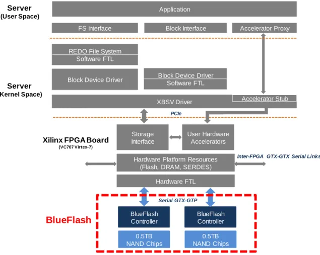
The hardware-software stack of BlueDBM is shown in Figure 1-2. BlueDBM provides three interfaces to the user application:
Inter-FPGA Network
PCIe High Speed Serial Link
Node 0 Node 1 Node n
…
FPGA Flash Host PC FPGA Flash Host PC FPGA Flash Host PC EthernetFigure 1-1: BlueDBM Architecture
1. A distributed file system interface: Using this interface, the underlying storage device appears as a unified store. Any existing application may operate on top of this interface without modification. To support this, BlueDBM runs a file system called REDO [33], which is a distributed flash-aware file system that works in concert with the reconfigurable flash controller to manage the underlying flash store.
2. A block interface: This lower level interface provides access to the storage blocks of the flash store. For applications that do not require files and manages its own data (e.g. a database), this interface provides a more direct path to storage with lower latency.
3. A hardware-software accelerator interface: This interface assists users in the integration of custom hardware accelerators into the system. In the hardware platform, we provide a method for user hardware accelerators to have direct access to the flash store to do in-store computation. In software, we expose a proxy-stub type interface from XBSV [15]. This allows user software to directly communicate with the accelerator.
Flash Controller
NAND Chips
User Hardware Accelerators
Hardware FTL Hardware Platform Resources
(Flash, DRAM, SERDES)
FlashBoard XilinxFPGABoard
(VC707 Virtex-7)
Server (Kernel Space)
Inter-FPGA Serial Links Application
Block Device Driver
XBSV Driver FS Interface
REDO File System Software FTL
Block Device Driver Software FTL
Block Interface Accelerator Proxy
Accelerator Stub Storage Interface Server (User Space) PCIe
Figure 1-2: BlueDBM Hardware Software Stack
In BlueDBM, flash management complexities are hidden from the user with the inclusion of a split hardware and software Flash Translation Layer (FTL). The soft-ware FTL is embedded in either the file system or the block device driver, and it is responsible for garbage collection and file segment mapping. The hardware FTL is a thin layer above the flash controller that handles wear-leveling and bad block management.
We note that BlueDBM overcomes the limitations that was mentioned in Section1.2. First, we leverage PCIe, thin XBSV drivers and a custom flash management inter-face to replace SATA3 and AHCI. Second, we use low latency serial links directly between flash devices for scaling and networking. Third, we introduce a flash-aware file system that cooperate with the hardware controller to manage flash. Finally, we expose simple interfaces for applications to perform in-store hardware accelerated computation.
1.4
Improving the BlueDBM Platform Hardware
A 4-node prototype of BlueDBM was constructed in 2012 and has shown excel-lent scalability and performance potential. However, the prototype was built using BlueSSD [32] boards that only provided 16GB of storage at 80MB/s. In compari-son, today’s PCIe SSDs are typically several terabytes in capacity with bandwidth of 1-3GB/s [4, 8]. Therefore, to construct a modern and usable BlueDBM platform to explore real Big Data problems at scale, we required an improved flash card and flash controller. Flash chips have evolved significantly since BlueSSD, and the following challenges have emerged:
1. Interface speed between NAND chips and controller have increased to several hundred MHz making precise signal skew adjustments and board trace matching a requirement.
2. As NAND density increases and NAND cells scale down in size, stronger bit error correction algorithms are required.
3. Number of buses and chips must quadruple compared to BlueSSD to reach terabytes of capacity and several GB/s of bandwidth.
4. Controller must keep up with the high data rate of the new NAND chips for best performance.
5. Tighter and stricter and timing requirements must be met.
Next, we introduce BlueFlash as the new high performance flash storage device for BlueDBM.
1.5
BlueFlash: A 0.5TB Flash Board and Controller
This thesis work presents BlueFlash, a revamped and improved storage device for the BlueDBM platform. We make the following contributions
2. We design and benchmark a new flash controller for the board capable of reach-ing 1.2GB/s
3. We explore the latency, error and power characteristics of the flash chips The portion of the BlueDBM platform in question is highlighted in Figure 1-3. The BlueFlash controller is situated beneath the hardware FTL layer in the stack, thus it does not manage NAND. Instead, it exposes command, address and data burst interfaces to access the flash chip array in a parallel and error-free manner. Its tasks are summarized below:
1. Communicate with each raw flash chip: data and command I/O, status moni-toring and initialization.
2. Calibrate timing and adjust skews 3. Correct page bit errors
4. Schedule commands for parallel access to multiple chips and buses
We are in the process of constructing a 16-node BlueDBM platform using 2 Blue-Flash boards per node. This provides 16TB of flash storage at approximately 38-51GB/s.
The rest of the thesis is organized as follows: Chapter 2 describes the flash board; Chapter 3 presents the flash controller design choices and implementation; Chapter 4 discusses the performance results of BlueFlash running on actual hardware; Chapter 5 talks about related work; Chapter 6 concludes with future work.
User Hardware Accelerators
Hardware FTL Hardware Platform Resources
(Flash, DRAM, SERDES) XilinxFPGABoard
(VC707 Virtex-7)
Server (Kernel Space)
Inter-FPGA GTX-GTX Serial Links Application
Block Device Driver
XBSV Driver FS Interface
REDO File System Software FTL
Block Device Driver Software FTL
Block Interface Accelerator Proxy
Accelerator Stub Storage Interface Server (User Space) PCIe BlueFlash Controller 0.5TB NAND Chips BlueFlash Controller 0.5TB NAND Chips BlueFlash Serial GTX-GTP
Chapter 2
BlueFlash Board Design
The BlueFlash board is the underlying flash storage device in BlueDBM. We expect to use the platform for the next 3-4 years in the exploration of Big Data applica-tions at scale. Thus we needed a competitive hardware platform that is feasible, cost effective and realistic in reflecting the state of flash storage in the current and near future markets. In the enterprise market, today’s state of art commercial flash drives are PCIe-based with capacities from 0.5TB to 3TB, achieving up to 2.7GB/s of bandwidth [4, 8]. We strive for similar performance and capacity for BlueFlash. The BlueFlash board also must provide support for the architectural ideas in BlueDBM. This includes sufficient reconfigurable fabric for hardware accelerator implementa-tion, direct serial links to other BlueFlash boards and an interface to servers via PCIe. With these goals in mind, we discuss the design choices of the board.
2.1
Flash Board Organization and Component Choices
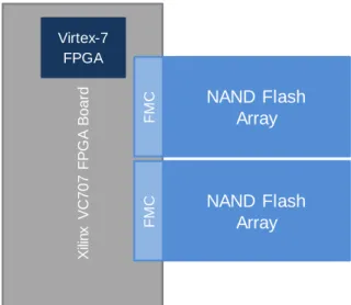
Since PCIe is required for the host to access the flash board, we chose to use an off-the-shelf Xilinx FPGA development board (VC707 [16]) as a cost-effective way to provide this interface. We call this board the carrier board. In addition the PCIe, the board provides a sizable Virtex-7 FPGA for accelerator implementation and on-board DRAM for caching. The BlueFlash boards will be an attachment to the carrier board via the FPGA Mezzanine Card interface (FMC) [17]. The FMC connector provides
high speed serial links as well as GPIO pins directly from the carrier FPGA. This organization is shown in Figure 2-1.
NAND Flash Array NAND Flash Array X ili n x V C 7 0 7 F P G A B o a rd F M C F M C Virtex-7 FPGA
Figure 2-1: FMC Flash Board Attached to Carrier Board
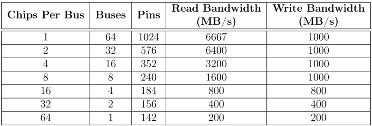
Today’s NAND packages are typically 64Gbits to 256Gbits in capacity. By them-selves, the chips are relatively slow, but by accessing them in parallel, we can aggre-gate to a significant amount of bandwidth. The common method to achieve this is by arranging chips into buses sharing common data and command signals (Figure 2-2). There are two levels of parallelism here:
1. Bus parallelism: Buses are independent, and can be addressed in parallel. 2. Chip parallelism: Chips on the same bus can be accessed in an interleaved
fashion to hide latency. For example, while one chip is busy performing a read, another chip can take control of the bus to stream back read data.
Bus parallelism is clearly preferred because buses are independent and we can achieve almost linear bandwidth scaling this way. However, increasing the number of buses also significantly increases the number of I/O pins on the controller. We can add more chips per bus to leverage chip parallelism, but this is only effective if the bus bandwidth has not saturated. Table 2.1 shows the different ways to arrange a 512GB flash card and the achieved theoretical performance. Calculation is made
Data Bus (8-bit) Command Bus
Chip Enable [0] Chip Enable [1]
NAND NAND
Figure 2-2: NAND Chip Connections on a Bus
based on Micron MLC flash with 8-bit wide data interface and 8KB pages operating at 100MHz DDR with read latency of 75𝜇s and program latency of 500𝜇s. We observe that we need 8 to 16 buses to be competitive with modern SSDs.
Chips Per Bus Buses Pins Read Bandwidth (MB/s) Write Bandwidth (MB/s) 1 64 1024 6667 1000 2 32 576 6400 1000 4 16 352 3200 1000 8 8 240 1600 1000 16 4 184 800 800 32 2 156 400 400 64 1 142 200 200
Table 2.1: NAND arrangements for a 512GB flash card
One design option is to connect these NAND buses directly to the FMC connector GPIOs, and program the flash controller on the carrier FPGA. However, the FMC has insufficient pins and this design also wastes valuable resources on the carrier FPGA that could be used for accelerator programming. Furthermore, because of the relative high bus speeds of modern NAND chips, signaling across the FMC connector could cause integrity problems. Instead, we chose to integrate a second smaller FPGA (Xilinx Artix-7) on the flash board. This FPGA contain the flash controller, and it communicates with the primary carrier FPGA using multiple high speed serial links (GTP). We chose an 8-bus, 8 chips per bus (with 4 chip dies per package), 512GB flash board design after factoring in cost, physical dimensions and I/O pin constraints.
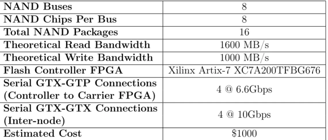
The specifications of the final flash board is outlined in Table 2.2, and the architecture diagram is shown in Figure 2-3.
NAND Buses 8
NAND Chips Per Bus 8
Total NAND Packages 16 Theoretical Read Bandwidth 1600 MB/s Theoretical Write Bandwidth 1000 MB/s
Flash Controller FPGA Xilinx Artix-7 XC7A200TFBG676 Serial GTX-GTP Connections
4 @ 6.6Gbps (Controller to Carrier FPGA)
Serial GTX-GTX Connections
4 @ 10Gbps (Inter-node)
Estimated Cost $1000
Table 2.2: FMC Flash Board Specifications
Finally, to create the sideband network directly between storage devices, the Blue-Flash board breaks out high speed serial connections (GTX) that is buried in the FMC connector of the carrier board as SATA ports. SATA cables are inexpensive and can run up to 1 meter in length.
A photo of the BlueFlash board and its corresponding layout is shown in Figure 2-4. Note that we use 2 flash boards per node.
SATA SATA
SATA SATA
SATA SATA
SATA SATA FMC
NAND NAND NAND NAND
NAND NAND NAND NAND
Artix-7 FPGA Bus 2 Bus 3 Bus 4 Bus 5
NAND NAND NAND NAND
Bus 6
Bus 7
NAND NAND NAND NAND
Bus 1
Bus 0 Chip 0,1 Chip 2,3 Chip 4,5 Chip 6,7
Controller to Carrier Serial GTX-GTP Inter-FPGA Serial GTX-GTX Artix-7 Serial GTP (Reserved)
X
ili
n
x
V
C
7
0
7
F
P
G
A
B
o
a
rd
Virtex-7
FPGA
F
M
C
Artix-7 FPGA NAND Array SATA SATAF
M
C
Artix-7 FPGA NAND Array SATA SATAChapter 3
BlueFlash Controller Design and
Implementation
As discussed in Section 1.5, the BlueFlash controller is a layer beneath the hardware FTL and its purpose is to provide a fast, parallel and error-free interface to the flash card with minimal bandwidth and latency overhead. Internally, the flash controller provides the protocols to communicate with individual flash chip, performs timing adjustments, corrects bit errors, and manages parallel accesses to multiple bus/chip. We first present the user interface of the flash controller (as used by the hardware FTL). Then we provide some background information on the NAND chips before discussing the design and implementation of the controller in detail.
3.1
Controller Interface
The flash controller interface is defined below in Bluespec:
interface FlashIfc;
method Action sendCmd (FlashOp op, Bit#(4) bus, Bit#(3) chip, Bit#(16) block, Bit#(8) page, Bit#(8) tag); method Action writeWord (Bit#(128) data, Bit#(8) tag);
method ActionValue#(Tuple2#(Bit#(128), Bit#(8)) readWord (); method ActionValue#(Bit#(8)) getWriteDataReq ();
The user of the flash controller is expected to have a multi-entry page buffer (256 entries or greater is recommended). Each entry of the buffer can hold an 8KB flash page and has a unique tag associated with it. This buffer will be used as a completion buffer for page reads, and as a write buffer to temporarily hold write data until it can be transferred. The operations (FlashOp) supported by the flash controller are read page, write page and erase block. We walk through each operation below.
∙ Page Read:
1. User allocates an entry in the page buffer
2. User sends the read request using the sendCmd method along with the unique tag associated with the page buffer entry from Step 1.
3. User continuously obtains 128-bit bursts of tagged read data using the readWord method. Each burst should fill the entry of the page buffer that has the corresponding tag.
4. When an entry of the page buffer fills, that particular page read operation is complete.
∙ Page Write:
1. Assuming the data to be written already occupies an entry in the page buffer, the user sends the write request (sendCmd method) with the asso-ciate tag of that entry.
2. The user monitors the getWriteDataReq method for a tag. Upon receiving a tag, the user sends an entry in the page buffer corresponding to that tag via the writeWord method in 128-bit bursts.
3. When the entire page buffer entry has been sent, the write is complete. ∙ Block Erase:
1. User sends the erase command using sendCmd with any tag (Don’t Care tag) and can consider the operation done.
Note that all methods enqueue into or dequeue from FIFOs, meaning that methods block when it is not ready, which could occur, for example, if the command queue is full or read data is not yet available.
The tagging scheme and page buffer is required because controller requests are often not executed in the order it was received. This is because internally, the flash controller contains a scoreboard that schedules each request in a way that maximizes bus utilization (discussed in Section 3.7). As a result, read data bursts corresponding to a particular request may arrive out of order and even interleaved with data from other requests, while write data for a particular request is not needed until the request is scheduled to be fulfilled. Unique tags help distinguish data of different requests.
3.2
Micron MLC NAND Chips
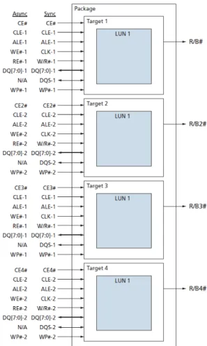
Before we delve into the controller design, we first present some basic details about the NAND chip on the flash board. We use Micron MLC NAND chips in a 256Gbit package with 4 dies per package. Its I/O interface is shown in Figure 3-1. The command interface consists of Address Latch Enable (ALE), Command Latch Enable (CLE), Write/Read (WR#) and Write Protect (WP#). The data interface consists of an 8-bit wide data port (DQ) and a Data Strobe (DQS). These signals are shared within a bus. The dies in the package are independently selected using the Chip Enable pin (CE#). In general, we use the 8-bit DQ port to send and receive bursts of data. This includes page data as well as controller requests and acknowledgments. The command interface latch enables are used to indicate the type of data that is being sent on the DQ port. The details of the communication protocol is defined by the Open NAND Flash Interface (ONFI 2.2) standard [18], which specifies timing requirements and command feature sets supported by the chip. The chip can operate at various speeds. The fastest mode is 100MHz, with DQ transferring at double data rate (DDR). This is also the speed of the NAND buses.
The access latencies of the chip are 75𝜇s for reads, 1300𝜇s for writes and 3.8ms for erases. This means that after requesting for read data at a particular address, the
controller must wait 75𝜇s before it can begin transferring read data from the NAND chip.
Figure 3-1: Micron MLC NAND Package
3.3
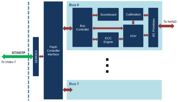
Architecture Overview
The architecture of the BlueFlash controller is shown in Figure 3-2. Data and com-mands are expected to arrive from the primary carrier Virtex-7 FPGA over serial GTX-GTP links to the flash board. The flash controller accepts these via the user interface defined previously, and distributes the request to multiple smaller indepen-dent bus controllers. As the name suggests, each bus controller manages a single bus containing 8 NAND targets that share a command (CLE, ALE, WR#, WP#) and data bus (DQ, DQS). The bus controller schedules commands by consulting a
scoreboard. Data to and from the NAND chips is passed through an ECC engine for encoding and decoding. Finally, the PHY communicates with the chips according to the timings set by the ONFI protocol. We discuss each block in detail below from right to left in the diagram.
GTX/GTP Bus 0 PHY ECC Engine I/O P ri m it iv e s Calibration Bus Controller S E R D E S Flash Controller Interface Scoreboard To Virtex-7 Bus 7
…
To NANDFigure 3-2: Flash controller architecture
3.4
NAND I/O Primitives
Similar to DRAM chips, modern NAND chips use synchronous DDR interfaces to communicate with its controller. This interface consists of a bidirectional data strobe (DQS) and a 8-bit wide data bus (DQ). The idea is that the sender of a data burst toggles DQS at the same rate and aligned to the DQ bus (Figure 3-3). The strobe serves as a validation indicator for the data. The receiver can then use the strobe as a clock to capture the data.
While fast, this interface presents timing challenges because factors such as drive strength, trace length, package skew, environment conditions, capacitance can all affect the rise and fall time of the signals. Thus sub-clock period timing adjustments on the data strobe is required to ensure that we are capturing valid data on the DQ
Data Data Data Data
CLK DQS DQ[7:0]
Figure 3-3: Synchronous DDR Data (DQ) and Strobe (DQS)
data bus. We make use of hard Xilinx FPGA primitives IDELAY, ODDR, IDDR and IOBUF to achieve this. The organization of the NAND I/O block for the DQ and DQS path is shown in Figure 3-4. The ODDR/IDDR primitives create DDR bursts on the bus, while IOBUF is a simple tristate buffer to handle the bidirectional bus. IDELAY allows for dynamic input delay adjustment from 0 to 5ns at 0.156ns increments. The delay tap value will be set by the calibration module.
Another timing challenge is the data strobe (DQS) to system clock domain cross-ing. DQS may have any phase relationship with respect to the internal FPGA system clock. Thus data captured using DQS cannot be directly used within the FPGA. Typ-ically for clock domain crossing, one can use synchronization flip-flops (e.g. SyncReg in Bluespec library) with handshaking or synchronization FIFOs (e.g. SyncFIFO). However, the former option does not work for crossing arbitrarily phase shifted clock domains that operate at the same frequency. The latter option also does not work because DQS is not an alway-on clock - it only toggles when data is transmitted and cannot be used to clock the synchronization FIFO further down the data pipeline. Instead, we sample the DQS captured data using 4 different phase shifted FPGA system clocks at 0∘, 90∘, 180∘ and 270∘ using a set of registers as shown in Figure 3-4. The calibration module (discussed in Section 3.5) determines the safest clock phase to use for domain transfer from DQS. We note that extra register stages were added to ensure that all data arrive at the same cycle and there is at least half a clock cycle of setup time (≥ 5ns) when transferring from one shifted clock domain to another.
D_RISE Q D_FALL IDELAY IOBUF ODDR IDDR D Q D Q D Q D Q D_RISE Q D_FALL IOBUF ODDR D Q D Q D Q D Q D Q D Q D Q D Q Q_RISE D Q_FALL DQS DQ 1 0 CLK_0 CLK_90 CLK_180 CLK_270 CLK_0 CLK_0 CLK_90 CLK_180 CLK_0 CLK_0 CLK_0 CLK_0 CLK_0 CLK_0 To similar set of registers Data_Out_Rise Data_Out_Fall Data_In_Rise
DQS Domain Transition System Clock
Domain
Calibrated_Sel
Figure 3-4: Controller NAND I/O Primitives
3.5
Read Capture Calibration
Because the chip timing takes on wide ranges and varies across different NAND chips, boards and buses, a dynamic read calibration algorithm is implemented to ensure that we capture valid data in synchronous mode. Calibration adjusts the following:
∙ Data to strobe delay (DQ-DQS phase)
∙ Read data capture domain crossing (DQS-to-FPGA clock) ∙ Read valid latency
The calibration algorithm works by reading a known training pattern from the NAND and performing adjustments until the pattern is seen by the controller. Since regular NAND pages can contain bit errors, reading patterns from them for calibration is not a good choice. Instead, we simply read the fixed NAND parameter page, which has enough bit pattern variations for calibration. The algorithm works as follows:
1. Request read on parameter page
2. Using 4 FIFOs, enqueue 32 cycles of read data captured at 4 different clock phases (0∘, 90∘, 180∘, 270∘) (Figure 3-4)
3. Keep a counter while dequeuing each FIFO and examining the data.
∙ If expected data pattern is seen on any of the 4 FIFOs, the counter tells us the read valid latency, while the FIFO that has the first burst of valid data tells us the approximate phase relationship between the data and system clock to allow us to select the correct phase for DQS-to-FPGA clock domain crossing.
∙ If we do not see expected data in the FIFO, the data to strobe alignment is wrong. Thus increment IDELAY on the DQS path and repeat Step 1.
We observe that there is a chance for setup/hold time violation if we sample the DQS clock domain data using 4 shifted FPGA clocks. For example, if the DQS-to-FPGA clock phase relationship is 91∘, metastability can occur on the register sampling the data using the 90∘ FPGA clock. However, we can simply tolerate this by choosing to always read the data using the register clocked 90∘ after observing the first valid burst of data. This way, regardless of the outcome of the metastable sample, we always have at least 2.5ns of setup time. We note that calibration is an iterative process that may take many cycles, but it is only done once at power on for each chip.
3.6
ONFI-compliant PHY
The BlueFlash PHY component is a large state machine that implements a sub-set of the ONFI protocol. The PHY can operate in two modes: asynchronous and synchronous. In asynchronous mode, controller and NAND chips are independently internally clocked, with no clock passed between them. Communication is done by waiting a fixed length of time after toggling command or data lines. This is a slow ac-cess mode (10MT/s) and the default power on mode. In synchronous mode, a clock is forwarded from the controller to the NAND chip (hence they are clock synchronous), and the strobe based DDR interface is the primary communication method. We can achieve 200MT/s this way.
In either mode, the PHY state machine implements 4 different communication cycles: command, address, data input and data output. Each type of cycle has strict timing requirements as specified by the datasheet. An example of a synchronous data output cycle is shown in Figure 3-5. By composing various PHY cycles together, we form a complete operation. For example, an erase block request from the user is composed of 1 command PHY cycle, 3 address cycles and 1 more command cycle in sequence.
3.7
Bus Controller and Scoreboard
The primary function of the bus controller is to break down requests (such as read page) into smaller PHY cycles (command, address, data input, data output) and issue them to the PHY. However, to achieve high bandwidth and low response time, chips must operate in parallel and the bus should be kept as busy as possible. We do this by interleaving PHY cycles of different requests and different chips on the bus. This behavior is shown in Figure 3-6.
A scoreboard is used to schedule PHY cycles onto the bus and track the status of each chip and request. The architecture of the scoreboard is shown in Figure 3-7. We create a request FIFO for each chip since requests aimed at a particular chip should
Figure 3-5: PHY Data Output Cycle
be executed in the order it was received (reordering is possible but requires checking for data hazards). In addition, for each chip, we keep a busy timer counter and a stage register. Upon receiving a request to read, write or erase, the bus controller immediately passes the request to the scoreboard. The scoreboard distributes the request to the appropriate chip request queue. The scheduler works in a round robin fashion. It picks the first serviceable request from the next chip and enqueues its next stage for execution. It then sets the busy timer to a predefined estimate of when the stage would be complete. Finally it updates the stage register to indicate which stage of the request it is currently on. It then moves to the next chip to schedule the next request. When the busy timer expires, the scheduler queues a request for the PHY to check if the chip has finished its job. If it has, the next stage is scheduled, otherwise the busy timer is set once again to further wait a predefined amount of time. When the request is complete, it is removed from the chip queue.
We make a few remarks about the scheduler. First, starvation of chips will not occur due to round robin scheduling. Second, we can only set an estimate of when a chip may complete its job because intrinsic NAND latencies can take on a large range.
tRead tRead tRead tRead tRead Single Chip Read Interleaved Multi-Chip Read
Command/Address Read Page Latency Data Transfer
Figure 3-6: Interleaving of NAND flash commands
For example, a block erase can take 3.8ms to 10ms [9] to complete. We must also poll the chip to obtain its status. The polling interval is a trade-off between wasting bus bandwidth and response latency. Finally, we note that the scheduler can have a notable performance impact depending on the workload. For example, a read-heavy latency-sensitive application may benefit from a scheduler that prioritizes short read operations over long erase and write operations.
3.8
ECC Encoder and Decoder
Bit errors are common occurrences in NAND flash chips, and error rate is influenced by many factors such as the number of P/E cycles, the value of the data and envi-ronment variables. ECC is a common technique to fix bit errors.
Commercial SSDs today use multiple levels of DSP techniques to correct errors. BCH codes or LDPC codes are commonly used [36]. Since we are building an ex-perimentation framework, long term reliability is not a priority. We chose to use Reed-Solomon codes since it consumes low resources on the FPGA, it is a common IP used on the FPGA and it just meets the minimum ECC requirement. Our MLC NAND chips require error correct capabilities of 24-bits per 1080 bytes of data [9]. A
Chip Current Request Request Stage Busy Timer 0 1 … 6 7
Scheduler
…
Chip 0 Chip 1 Chip 7
Figure 3-7: Scoreboard architecture
common Reed-Solomon decoder is 𝑅𝑆(𝑛, 𝑘) = 𝑅𝑆(255, 223) with 16B parity (6.3%), but this configuration exceeds flash page capacity. Each MLC flash page contains 8192B of user data with 448B (5.2%) provisioned for ECC parity bytes. We adjust the decoder to be 𝑅𝑆(255, 243) with 12B parity (4.7%). This allows us to correct 6 word and detect 12 word errors per 255B block. This is approximately equivalent to 24-bit ECC per 1020B of data and thus meeting the requirement. Note that this equivalence only holds because NAND bit errors tends to be uniformly distributed across a page (i.e. Seeing 24 bit errors bunched together is rare). We used a modified ECC decoder from Agarwal et al. [20]. Details of the decoder is beyond the scope of this thesis. The encoder block follows a standard design [25] and is shown in Fig-ure 3-8. It is fully pipelined and uses the standard generator polynomial coefficients
for 𝑡 = 6 obtained using Matlab.
Figure 3-8: Reed Solomon encoder architecture (shrunken version with 4 word blocks)
For each bus, we integrated two pairs of encoder-decoders in parallel since the NAND bus is 16-bit wide (after DDR) while encoder-decoders words are 8-bits wide. On each page reads and writes we process the data in 255B blocks (zero pad the last block). We add large page-sized buffers before and after the encoder-decoders because for PHY DDR write bursts to the chips, new data must be available each cycle. Similarly on read DDR bursts, there must be space to accept the data.
We observe that ECC can add significant latency because of: (i) pipeline delay and (ii) if there are bit errors, the pipeline can stall for hundreds of cycles while iterative algorithms in the decoder (i.e. Chien Search and Berlekamp) identifies the error. This is explored in Section 4.5.
3.9
Flash Controller
The top level flash controller instantiates all 8 bus controllers. It forwards commands to each bus controller and aggregates data bursts into 128-bit words for the user or splits them for the controller.
3.10
Serializer/Deserializer
The flash board acts as a slave storage device to the master carrier FPGA on the Xilinx VC707 board. We use high speed GTX-GTP serial links for communication between the primary Virtex FPGA and the flash controller on the Artix FPGA. The communication IP is the Xilinx provided Aurora protocol. The flash controller’s interface is "forwarded" to the primary FPGA via Aurora and the serial links for the hardware FTL and accelerators running on the primary FPGA.
Chapter 4
Verification and Evaluation
In this chapter, we discuss the functional verification methods used for the BlueFlash controller, and we evaluate the performance of both the controller and the NAND chips.
4.1
Development Tools
The flash controller was developed using both Verilog and Bluespec Verilog. We used Verilog to instantiate Xilinx FPGA primitives and low level timing logic in the NAND I/O Primitive module (Figure 3-4). All other modules were written in Bluespec. The source code for the controller is available on Github[1]. Xilinx Vivado 2014.2 was used for synthesis, implementation, simulation and debugging on the FPGA.
4.2
Verification and Test Setup
It is difficult to identify timing violations on actual hardware because metastability may cause rare and random failures. Thus we used Vivado XSim to first perform timing simulations of the controller. A testbench was setup containing the flash con-troller connected to Verilog models of the NAND chips provided by Micron. Since the data (DQ) and data-strobe (DQS) path is sensitive to sub-clock-cycle skews, we created post-place-and-route timing simulations to test the robustness of the
calibra-tion algorithm. We verified that the calibracalibra-tion algorithm correctly adjusts the delay to compensate for a wide range of DQ-DQS skews.
For verification of the entire controller, we created a traffic generator and a data checker module attached to the flash controller. The traffic generator issues read, write and erase requests to the controller, using data that was generated by hashing the address of the request. When the data is read back, the checker module rehashes the address to verify that it matches with the expected data. The hash function ensures that different data will be written to each page, block, chip and buses of the flash array. In addition, it creates data bursts that have high toggle rates, which helps to bring out any potential timing errors.
For benchmarking, we added performance counters to measure the data flow and latency. Vivado Chipscope Analyzer was used to select the test suite and retrieve performance data.
4.3
Resource Usage
The design uses about half of the resources on the Artix-7 FPGA for all 8 buses: 20% Flip-flops, 49% LUTs and 53% BRAM, and 47% of I/O pins. A breakdown of the resource usage is shown in Table 4.1.
Module Name # of Modules LUTs Registers BRAM Bus Controller 8 7131 4870 18 → ECC Decoder 2 1790 1233 2 → Scoreboard 1 1149 780 12 → PHY 1 1635 607 0 → ECC Encoder 2 565 222 0 Total 65457 (49%) 55061 (20%) 192 (53%) Table 4.1: Resource Usage of Key Modules
We observe that within each Bus Controller, the Reed-Solomon decoder accounts for a large portion of the LUTs since it is arithmetic heavy. The scoreboard also uses significant resources because it is a shared structure that multiplexes between buses. The large state machine in the PHY is next on the list. Finally, a large portion of
BRAMs and Registers are used as FIFOs to buffer read/write data back-pressure in the pipeline.
The controller operates at the same speed as the NAND chips: 100MHz.
4.4
NAND Page Bit Errors
Bit errors are common occurrences in NAND cells and they are one of the major downsides of NAND flash. Error rate can easily reach the range of 10-2, and is
affected by the number of P/E cycles, the number of bits stored per cell, interference from operations on neighboring pages, the value of data written, the location of the page/block and many other factors [22]. A full characterization of NAND errors is beyond the scope of this work. However, since the number of errors affect the performance of the ECC decoder, we briefly look at the error rate of our BlueFlash NAND chips. Figure 4-1 shows the percent occurrence distribution of the number of errors per 8KB page from writing/reading random data at random addresses. On average, we observe 2.18 bit errors per page for these new MLC flash chips, which should have a relatively small impact on performance since it means most ECC blocks are error free. Our ECC algorithm is able to correct approximately 102 bit errors per page (as discussed in Section 3.8).
4.5
Access Latency
We define read access latency as the time it took to receive the data for an entire page after issuing a single read page request. Write access latency is similarly defined as the time between issuing the write request (with write data) and receiving an acknowledgment from the controller that the operation is complete.
4.5.1
Read Latency
The read latency breakdown is shown in Figure 4-2. The NAND latency of 70𝜇s is within the expected range (datasheet claims <75𝜇s). With 8K pages (8600B including
10.3% 25.6% 28.2% 17.9% 10.3% 5.1% 2.6% 0.0% 5.0% 10.0% 15.0% 20.0% 25.0% 30.0%
0
1
2
3
4
5
> 6
% O c c u re n c eNumber of Bit Errors Per Page
Figure 4-1: Bit Errors Per Page Distribution (% Occurrence)
ECC) transferring at 8-bit wide 100MHz DDR, this page transfer process also incurs a significant 43𝜇s of latency. The ECC decoder latency varies with the number of errors to correct. The current 2.18 bit errors per page (Figure 4-1) translates into only 4𝜇s of latency, but this is expected to increase as the chips age. Command latency is insignificant. In total, the read latency is 117𝜇s.
0 20 40 60 80 100 120 140
Read Latency
Latency (us)
Command & PHY NAND Latency Data Transfer ECC
Figure 4-2: Read Access Latency Breakdown
4.5.2
Write Latency
The write latency breakdown is shown in Figure 4-3. Although the data sheet claims typical program latency of 1300𝜇s, we measure only 420𝜇s on the board. Again, page data transfer incurs 43𝜇s of latency. The ECC encoder is fully pipelined with no stalls
and incurs constant and insignificant delay.
0 50 100 150 200 250 300 350 400 450 500
Write Latency
Latency (us)
Command & PHY NAND Latency Data Transfer ECC
Figure 4-3: Write Access Latency Breakdown
4.6
Bandwidth and Scaling
We examine the ability of the controller to extract parallelism out of the NAND chips and buses to evaluate its efficiency. We emulate sequential read and write of a 128MB chunk of data spread among the chips and buses of the board.
4.6.1
Chips Per Bus Scaling
Figure 4-4 shows the bandwidth scaling on a single bus with increasing number of chips per bus. We observe that the read bandwidth saturates after 2 chips per bus at 150MB/s. This can be explained by the latency breakdown (Figure 4-2). The bus is held by a chip only during command and data transfer ( 43𝜇s) phases, while in between when this chip is busy ( 75𝜇s), other chips can use the bus. This allows 2 chips to comfortably share the bus without saturating it. However, with 4 or 8 chips, the bus saturates and there is contention. Furthermore, because of round robin scheduling, read request commands ( 1𝜇s per command), status polling ( 1𝜇s per poll) and data transfer (43𝜇s) all have fair access to the bus. This means that the read request could potentially be sent later than optimal. Moreover, the bus saturates at a theoretical max of 200MB/s, which could exceed the ECC decoder’s capabilities if there are many errors in the page. Finally, ECC parity inherently introduces a 5% overhead since we transfer 8600B of data, but only 8192B are useful. For these reasons, we end up achieving a still respectable 150MB/s per bus or 75% of the theoretical max bus bandwidth.
For writes, because of long NAND chip program latency of 420𝜇s (Figure 4-3), the bus does not saturate with 8 chips, and we achieve almost linear scaling with more chips. The theoretical max speed is 138MB/s if we assume perfect parallelism at the measured program latency. The actual speed of 126MB/s with 8 chips is 91% of that.
68.0 135.2 128.3 149.2 16.8 29.3 59.0 125.9 0.0 20.0 40.0 60.0 80.0 100.0 120.0 140.0 160.0
1
2
4
8
B a n d w id th ( M B /s )Chips Per Bus
Read Write
Figure 4-4: Bandwidth Scaling by Number of Chips Per Bus
4.6.2
Number of Buses Scaling
Figure 4-5 shows the bandwidth scaling when multiple buses operate in parallel, with 8 chips per bus. Since the buses are mostly independent, sharing only the incoming command FIFO, we have linear scaling for both reads and writes. Overall, when all chips and buses are used, the flash board and controller are able to reach approximately 1.2GB/s read and 1.0GB/s write bandwidth, or with 2 boards per node, 2.4GB/s read and 2.0GB/s write bandwidth - competitive with modern PCIe SSDs.
148.9 297.6 595.4 1194.2 125.7 246.7 490.9 980.6 0.0 200.0 400.0 600.0 800.0 1000.0 1200.0 1400.0
1
2
4
8
B a n d w id th ( M B /s ) Number of BusesRead Write
Figure 4-5: Bandwidth Scaling by Number of Buses
4.7
Power Consumption
We measured the total power consumption of the flash board at the power supply source, and the FPGA portion of the power using the on-board TI UCD9090 power sequencer. Measurements were taken when (i) the Artix-7 FPGA is not programmed (i.e. NAND chip idle power only); (ii) the Artix-7 is programmed and idle after ini-tializing the NAND chips; (iii) during continuous sequential read operations. Results are shown in Figure 4-6. We observe that the NAND chips idle at approximately 1.5W, and consumes 3.7W (60% of total) during read operations. The FPGA con-troller consumes 1.5W during idle and 2.4W (40% of total) during reads. We note that power optimization techniques such as clock gating and power gating have not been used in the controller implementation. In total, we consume 6W of power during reads. In comparison, the modern consumer Samsung SATA SSDs consume merely 4W of peak power[35], but larger enterprise PCIe SSDs can consume 30W[8], and enterprise hard disks can consume 10W of power[13] (at much lower performance). Of course, power is heavily influenced by the number of NAND packages and the process node the chips are made. We estimate that with 2 BlueFlash boards per
node, together with the carrier board PCIe core, the power consumption would be in the range of 15-20W. This is competitive, if not better, than many enterprise PCIe SSDs on the market.
0 1 2 3 4 5 6 7
Sequential Read FPGA Controller Idle FPGA Not Programmed
Power Consumption (W)
FPGA NAND + Other Components
Chapter 5
Related Works
BlueSSD [32] was the flash storage device used on the initial BlueDBM prototype. Designed in 2009, it was also an FMC attachment flash card with an FPGA-based flash controller. While modern at its time, the boards are only 16GB in capacity, operated at 80MB/s with 4 buses, and used much slower and higher latency ECC-embedded asynchronous NAND chips. The BlueSSD board did not have a secondary FPGA because there were enough GPIO pins for 4 NAND buses on 2 FMC ports. The BlueSSD controller did not require ECC, a synchronous PHY or timing calibration. In contrast, on 2 FMC ports, the BlueFlash board has 16 buses and reads at 2.4GB/s. Most SSD controllers today are ASICs, typically embedded with multiple ARM cores [12, 7]. As explained in Chapter 1, they expose an abstracted block device view to the system, hiding all of the flash management. In BlueDBM, we embrace flash as the storage device and expose the chips, blocks and buses to the operating system and use a flash aware file system with a hardware accelerated FTL to more efficiently manage flash. FPGA SSD controllers have been used in enterprise PCIe SSDs because of their low development cost and fast time to market [2, 4]. However, these FPGAs have not been used in the context of building accelerators and a dedicated sideband storage network.
Recent efforts such as CORFU [21] attempts to build distributed file systems tailored for flash storage characteristics, but still suffers millisecond-level latency. Other attempts such as QuickSAN [23] have studied directly connecting flash storage
to the network in order to bypass some of the software latency. This brings down the latency of the system to hundreds of microseconds. BlueDBM aims to further improve performance by removing protocol and software overhead.
FPGAs have been gaining popularity as application specific accelerators for Big Data due to its low power consumption, flexibility and low cost. FPGA accelera-tors are currently being used in database management systems [5], in providing web services [24], as well as in other domains such as machine learning [34] and bioinfor-matics [37].
Chapter 6
Conclusion and Future Work
In this thesis, we presented BlueFlash, a 0.5TB flash card and a reconfigurable flash controller for the BlueDBM platform. We were able to achieve 1.2GB/s read band-width (75% of theoretical max) and 1.0GB/s of write bandband-width (91% of theoretical) at latencies of 117𝜇s and 462𝜇s respectively for read and write. We showed that the controller scales well with number of chips per bus and number of buses, up until the bus saturates.
There are several potential improvements to the design that may further improve bandwidth and latency:
1. Priority-based scheduler: Instead of using a simple round robin scheduler, we can choose to prioritize shorter transfers on the bus such as request com-mands and status polls. This could lead to better response time and less idling for the chips.
2. Read/Write latency calibration: Polling for chip status is a waste of pre-cious bus bandwidth. Currently the polling interval is statically set. Instead of polling for the completion of each command, we can use the latency of the first read/write/erase command to estimate the latency of the subsequent com-mands. Using this information to set the busy timer counter in the scoreboard could lead to less polling.
alleviate pipeline stalls that would prevent later pages from being decoded in the case there are bit errors.
Other future work include the development of the hardware FTL to work in concert with the flash aware file system.
Bibliography
[1] BlueFlash Controller. https://github.com/m-liu/NandController. Accessed: Aug. 2014.
[2] FusionIO. http://www.fusionio.com. Accessed: Aug. 2014.
[3] Hadoop Distributed File System. http://hadoop.apache.org/docs/ stable/hdfs_user_guide.html. Accessed: Aug. 2014.
[4] HGST FlashMax III PCIe Enterprise Solid-State Drives. http://www.hgst.com/tech/techlib.nsf/techdocs/
BBA40DB8DB897C8288257D250004E803/%24file/ FlashMAX-III-PCIe-SSD-DS.pdf. Accessed: Aug. 2014.
[5] IBM Netezza. http://www-01.ibm.com/software/data/netezza/. Accessed: Aug. 2014.
[6] Lustre. http://wiki.lustre.org/index.php/Main_Page. Accessed: Aug. 2014.
[7] Marvell 88NVM9145 NAND Flash Controller. http://www.marvell. com/storage/system-solutions/native-pcie-ssd-controller/ assets/Marvell-88NV9145-Prod-Brief.pdf. Accessed: Aug. 2014. [8] Micron Enterprise PCIe SSD. http://www.micron.com/products/
solid-state-storage/enterprise-pcie-ssd#fullPart&306=1. Accessed: Aug. 2014.
[9] Micron MT29F256G08CMCABH2 Data Sheet. http://www.micron.com/ parts/nand-flash/mass-storage/mt29f256g08cmcabh2-10z?pc= {36C90F35-E056-45D2-B329-7EDCE578C1BA}. Accessed: Aug. 2014. [10] NFS Specifications. http://tools.ietf.org/html/rfc1094. Accessed:
Aug. 2014.
[11] PureStorage FlashArray. http://www.purestorage.com/flash-array. Accessed: Aug. 2014.
[12] SandForce Flash Controllers. http://www.lsi.com/products/ flash-controllers/pages/default.aspx. Accessed: Aug. 2014.
[13] Seagate Enterprise Performance 10K HDD. http://www.seagate. com/internal-hard-drives/enterprise-hard-drives/hdd/ enterprise-performance-10K-hdd/#specs. Accessed: Aug. 2014. [14] Violin Memory. http://www.violin-memory.com. Accessed: Aug. 2014. [15] Xbsv. https://github.com/cambridgehackers/xbsv. Accessed: Aug.
2014.
[16] Xilinx Virtex-7 FPGA VC707 Evaluation Kit. http://www.xilinx.com/ products/boards-and-kits/EK-V7-VC707-G.htm. Accessed: Aug. 2014.
[17] FPGA Mezzanine Card Standard. http://www.xilinx.com/support/ documentation/white_papers/wp315.pdf, August 2009. Accessed: Aug. 2014.
[18] Open NAND Flash Interface Specification. http://www.onfi.org/-/ media/onfi/specs/onfi_2_2%20gold.pdf, October 2009. Accessed: Aug. 2014.
[19] NVM Express. http://www.nvmexpress.org/wp-content/uploads/ NVM_Express_1_1b.pdf, July 2014. Accessed: Aug. 2014.
[20] A Agarwal, Man Cheuk Ng, and Arvind. A comparative evaluation of high-level hardware synthesis using reed-solomon decoder. Embedded Systems Letters, IEEE, 2(3):72–76, Sept 2010.
[21] Mahesh Balakrishnan, Dahlia Malkhi, Vijayan Prabhakaran, Ted Wobber, Michael Wei, and John D. Davis. Corfu: a shared log design for flash clusters. In Proceedings of the 9th USENIX conference on Networked Systems Design and Implementation, NSDI’12, pages 1–1, Berkeley, CA, USA, 2012. USENIX Asso-ciation.
[22] Yu Cai, Erich F. Haratsch, Onur Mutlu, and Ken Mai. Error patterns in mlc nand flash memory: Measurement, characterization, and analysis. In Proceedings of the Conference on Design, Automation and Test in Europe, DATE ’12, pages 521–526, San Jose, CA, USA, 2012. EDA Consortium.
[23] Adrian M. Caulfield and Steven Swanson. Quicksan: a storage area network for fast, distributed, solid state disks. In Proceedings of the 40th Annual Inter-national Symposium on Computer Architecture, ISCA ’13, pages 464–474, New York, NY, USA, 2013. ACM.
[24] Sai Rahul Chalamalasetti, Kevin Lim, Mitch Wright, Alvin AuYoung, Parthasarathy Ranganathan, and Martin Margala. An fpga memcached ap-pliance. In Proceedings of the ACM/SIGDA international symposium on Field programmable gate arrays, FPGA ’13, pages 245–254, New York, NY, USA, 2013. ACM.
[25] C.K.P Clarke. Reed-Solomon error correction. http://downloads.bbc.co. uk/rd/pubs/whp/whp-pdf-files/WHP031.pdf, July 2002. Accessed: Aug. 2014.
[26] Danny Cobb and Amber Huffman. NVM Express and the PCI Express SSD Revolution. http:// www.nvmexpress.org/wp-content/uploads/2013/04/
IDF-2012-NVM-Express-and-the-PCI-Express-SSD-Revolution. pdf, May 2012.
[27] Peter Desnoyers. Empirical evaluation of nand flash memory performance. SIGOPS Oper. Syst. Rev., 44(1):50–54, March 2010.
[28] Sanjay Ghemawat, Howard Gobioff, and Shun-Tak Leung. The google file sys-tem. In Proceedings of the nineteenth ACM symposium on Operating systems principles, SOSP ’03, pages 29–43, New York, NY, USA, 2003. ACM.
[29] Intel. Serial ATA AHCI. http://www.intel.com/content/dam/ www/public/us/en/documents/technical-specifications/
serial-ata-ahci-spec-rev1-3-1.pdf, June 2008. Accessed: Aug. 2014.
[30] Jisha J. Achieving a High Performance OLTP Database using SQL Server and Dell PowerEdge R720 with Internal PCIe SSD Storage. http://www.dell.com/downloads/global/products/pvaul/en/ sql-server-perf-with-express-flash-and-poweredge-r720. pdf, March 2012.
[31] Sang-Woo Jun, Ming Liu, Kermin Elliott Fleming, and Arvind. Scalable multi-access flash store for big data analytics. In Proceedings of the 2014 ACM/SIGDA International Symposium on Field-programmable Gate Arrays, FPGA ’14, pages 55–64, New York, NY, USA, 2014. ACM.
[32] S. Lee, K. Fleming, J. Park, K. Ha, A. Caulfield, S. Swanson, Arvind, and J. Kim. Bluessd: An open platform for cross-layer experiments for nand flash-based ssds. In The 5th Workshop on Architectural Research Prototyping, WARP, 2010. [33] S. Lee, J. Kim, and A Mithal. Refactored design of i/o architecture for flash
storage. Computer Architecture Letters, PP(99):1–1, 2014.
[34] Karthik Nagarajan, Brian Holland, AlanD. George, K.Clint Slatton, and Herman Lam. Accelerating machine-learning algorithms on fpgas using pattern-based decomposition. Journal of Signal Processing Systems, 62(1):43–63, 2011.
[35] Christopher Ryan. Samsung 840 EVO SSD. http://www.tomshardware. com/reviews/samsung-840-evo-review-1tb-ssd,3567-13.html, July 2013. Accessed: Aug. 2014.
[36] Eran Sharon, Idan Alrod, and Avi Klein. ECC/DSP System Architecture for Enabling Reliability Scaling in Sub-20nm NAND. http://www.bswd.com/ FMS13/FMS13-Klein-Alrod.pdf, August 2013. Accessed: Aug. 2014. [37] Fei Xia, Yong Dou, Guoqing Lei, and Yusong Tan. Fpga accelerator for protein
secondary structure prediction based on the gor algorithm. BMC Bioinformatics, 12(Suppl 1):S5, 2011.