HAL Id: hal-00385937
https://hal.archives-ouvertes.fr/hal-00385937
Submitted on 10 Mar 2020HAL is a multi-disciplinary open access
archive for the deposit and dissemination of
sci-L’archive ouverte pluridisciplinaire HAL, est destinée au dépôt et à la diffusion de documents
Nanoimprint lithography: full wafer replication of
nanometer features
R. Pelzer, C. Gourgon, S. Landis, P. Kettner
To cite this version:
R. Pelzer, C. Gourgon, S. Landis, P. Kettner. Nanoimprint lithography: full wafer replication of nanometer features. SPIE 2005, 2005, Sydney, Australia. pp.256-259, �10.1117/12.582435�. �hal-00385937�
Nanoimprint Lithography -
Full Wafer Replication of Nanometer Features
Rainer Pelzer
1, Cécile Gourgon
2, Stefan Landis
3, Paul Kettner
11
EV Group, DI Erich Thallner Strasse 1, A-4780 Schaerding, Austria
E-Mail: [email protected], Phone: +43 7712 5311-0, Fax: +43 7712 5311-4600
2
Laboratoire des Technologies de la Microelectronique – CNRS, 17 R. des Martyrs (CEA-LETI),
F-38054 Grenoble Cedex, France
3
CEA-LETI, 17 R. des Martyrs, F-38054 Grenoble Cedex, France
ABSTRACT
Nanoimprint Lithography (NIL) is a fast, high resolution replication technology for micromechanics, microbiology and even for microelectronic applications in the sub-100nm range. The technique has been demonstrated to be a very promising next generation technique for large-area structure replication up to wafer-level in the micrometer and nanometer scale. For producing nanometer structures the capital investments required are much lower compared to other next generation methods (e-beam writing, x-ray lithography, EUV lithography, …).
Nanoimprint Lithography is based on two different techniques: Hot Embossing (HE) and UV-Nanoimprint Lithography (UV-NIL). Both methods can be used for replicating dense and isolated features in the range of 70nm to 100µm simultaneously on up to 200mm wafers.
Key Words
Nanoimprinting, Hot Embossing, UV-Nanoimprint Lithography, Sub-100nm features
1 INTRODUCTION
Hot embossing (HE) is a technique where three-dimensional pattern definitions with structured silicon or metal stamps (LIGA) are achieved on polymers or polymer coated wafers at elevated temperature under pressure. This method allows further rapid prototyping or high volume production of fully patterned substrates for a wide range of materials.
UV-NIL is totally different from the perspective of process parameters and therefore the equipment solution. A lot of research has been conducted in the field of UV-NIL. This technique has demonstrated a high potential for large area definitions of nm scaled
patterns at low cost. For UV-Nanoimprint Lithography (UV-NIL) or Mold Assisted Lithography (MAL) a UV resist is cured with UV light at RT under low contact force after imprinting with a transparent stamp.
The advantages of using polymer substrates, making them suitable for use in micro- and nano-fabrication are: bio-compatible surfaces, easy manufacturability, low cost and high volume production, a broad range of different optical, mechanical, chemical or electrical properties (transparency, conductivity, softness) just to name a few. Thus, embossing can be applied in a wide variety of fields: µ-TAS, biochemistry, chemistry, life science, micro-optical applications, nano-fluidics, data storage, etc.
We will present all three techniques and experimental results on all processes with PMMA (NEB22, mr-I
8030) and different UV resists. Results on full wafer imprints up to 200mm with high-resolution patterns for microelectronic applications will be presented in this paper.
2 HOT EMBOSSING
Printing results have been demonstrated on wafers up to 100mm with a few patterns distributed across the stamp surface in the past [1]. This work focuses on transferring dense structures, with different feature sizes from 70nm to 100µm, simultaneously from a 200mm stamp into different thermoplastic polymer layers.
The key parameters for HE are: cycle time, imprint uniformity, repeatability from wafer to wafer, reproducibility and contour accuracy of features across the full wafer diameter, minimum feature sizes vs. highest aspect ratio and de-embossing utilizing anti-sticking layers.
2.1 Process and Cycle Time
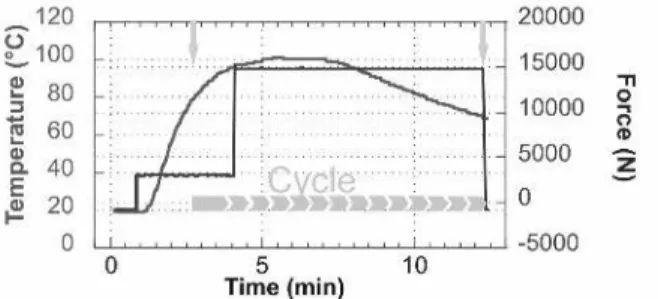
The cycle time of an imprinting process (example shown in Fig. 1) is mainly depending on the glass transition temperature of the polymer and the thickness of the polymer. The first process step is the evacuation of the HE-chamber. A vacuum level of below 0,01mbar was evaluated, to be required, in order to prevent air encapsulation in the stamp structure during the imprinting step.
Figure 1: Cycle time of a NEB22 imprint process
Fig. 2a and 2b demonstrate the importance of this process step. The figure shows dense 250nm features, structured at ambient pressure and in vacuum of 10-2 mbar. The structure in Fig. 2b is the true inverse contour, full replication of the stamp structure, whereas the patterns in Fig. 2a are completely destroyed by the escaping air during the imprinting step.
Figure 2: Replication results of 250nm lines in NEB22 a) at ambient pressure and b) at a vacuum level of 0,01mbar
In the second process step the polymer carrier and the stamp are heated to several degrees above the glass transition temperature of the polymer. This glass transition temperature is corresponding to the molecular weight M of the polymer chains. It’s defined as the temperature range, where the shear modulus G of the polymer decreases rapidly (for PMMA: from ~1000N/mm² down to 1N/mm²). For polymers with low molecular weight, the shear module declines further at increasing temperature. Thermoplastics with high M form a plateau in the range of several decades in °C before the shear module decreases further into the thermoplastic state (yield point). For PMMA the values can be found as: Tg = 105°C for PMMA with a degree
of polymerisation P=MPMMA/MMMA~750 (molecular
weight of the macro molecules MPMMA
~70000-100000g/mol; molecular weight of the monomer MMMA)
and Tg = 60°C for PMMA with P~60 (molecular weight
of ~ 6000g/mol). Below this value of P the glass transition temperature is independent of the molecular weight.
NEB22 and mr-I 8030 are polymers based on aromatic MMA (methyl methacrylate). The mr-I 8000 polymers from MicroResist Technology are designed for HE applications. mr-I 8030 is delivered, solved in an organic solvent and has a molecular weight of around 4.105g/mol. After spinning it onto a wafer at 3000rpm for 30sec and drying at 140°C the remaining polymer layer has a thickness of around 300nm. The glass transition temperature is between 110-120°C. NEB22 is a high-resolution chemical amplified e-beam resist from Sumitomo Chemical. The resist is distinguished by its low glass transition temperature (~80°C) and very well understood physical and chemical properties [2]. The third step is the imprinting step at high contact forces. In this process step the polymer is pressed into the stamp relief. In order to protect the stamp structure from damage, direct contact between stamp and the rigid polymer carrier must be prevented. Therefore a residual thickness of several hundred nm should remain underneath the imprinted features. NEB22 is imprinted at around 100-130°C and 15-25kN for 5 minutes. The process parameters for replicating the same features into mr-I 8030 was also investigated. The imprinting temperature was set to 175°C and contact force to 20kN. The imprinting results of the two resist are very similar. There is a lot of development work going on with low Tg polymers [3].
2.2 Uniformity control and mold deformation
The control of the residual thickness hr is the most
significant and accurate way of evaluating the uniformity and performance of the equipment. Fig. 3 demonstrates the characteristics of the residual thickness, measured in similar features across a 200mm wafer. The table shows that the thickness variation is smaller than ±10nm (except outlier value 10, which was caused by an vacuum groove cutout in the exclusion zone of the pressure chuck).
It could be demonstrated, that higher contact forces (for the configuration stamp and polymer carrier both made of silicon) have a significant influence to the residual thickness uniformity. The different curves in Fig. 4 give account of the residual thickness for different
feature densities at contact pressures of 15, 25 and 50bar.
Figure 3: Uniformity control of imprints across 200mm wafers by measuring the residual thickness hr [Figure Courtesy of CNRS-LTM and CEA-LETI]
With a contact pressure of 50bar, the total residual thickness variation in the dense pattern region is almost 5 times higher than the residual thickness variation at 15bar.
Figure 4:Contact pressure optimisation on 500nm aperiodic L/S [Figure Courtesy of CNRS-LTM and CEA-LETI]
2.3 Replication: reproducibility, feature size and aspect ratio
The following three SEM pictures (Fig. 5-7) demonstrate how accurate the contours of the patterns can be replicated on 200mm wafers with this technique. Fig. 5 shows a printed hole array with 110nm holes and 80nm lateral with. The aspect ratio is 1:3. Fig. 6 shows the inverse structure of Fig. 5. The polymer dots have an aspect ratio of 1:1 and a diameter of 85nm.
The two pictures in Fig. 7 give account of the excellent replication of dense L/S features in the sub-100nm range. Even the sidewall roughness of the e-beam
structured Si stamp was transferred into the polymer (see inset figure).
Figure 5: 110/80nm holes imprinted in NEB22
Figure 6: 100nm high dots with 85nm in diameter and a pitch of 75nm imprinted in NEB22
Figure 7: 110/80nm lines and spaces and close look up onto 250nm L/S imprinted into NEB22
2.4 Equipment
On the EVG®520HE Hot Embossing system, the temperature uniformity across the 200mm wafer for up to 350°C is below ±1°C. Top and bottom heater are independently temperature controlled, in order to use dissimilar materials of stamp and substrate. The applied contact force can be varied from 500 up to 40000N.
3 UV-NANOIMPRINT LITHOGRAPHY
The second large area imprinting process, which is discussed in this paper, is the UV NanoImprint Lithography (UV NIL). The process differs from HE; monomers, which are cured induced by polymerisation under UV light, are utilized for this 3D structuring technique. This low-viscosity UV-curable resists allow processes to run under room temperature and very low contact forces. Therefore this method realizes very short process times and less stamp abrasion. The stamps have to be transparent to allow the UV light to polymerize the resist of the interface stamp-substrate. The utilized stamp materials are either quartz or poly(dimethylsiloxane) (PDMS) [4]. The attractive properties of structured PDMS stamps are low interfacial free energy (22-24dyn/cm), high optical UV transparency (>85% @ 340-600nm), good chemical stability and the soft, elastomeric behaviour. This soft character enables to imprint monomers on nonplanar surfaces. On the other side the contact force must be controlled very accurately, due to mold structure deformation during the imprint step.
3.1 Soft stamp fabrication and process
PDMS-stamps can be fabricated by cast molding from etched Si masters (130°C; 30min). After separation from the master, the backside of the formed PDMS stamp has to be treated for 30-60sec with oxygen plasma, in order to transform the hydrophobic surface character into a hydrophilic one. The PDMS can now be bonded to a quartz carrier.
The UV-molding process is performed in a NIL alignment system, the EVG®620NIL, where the stamp and the substrate are optically aligned with sub-µm alignment accuracy. The process flow is as follows: a monomer coated carrier substrate (e.g. silicon wafer) as well as the transparent stamp are loaded into the aligner and fixed on their respective chucks. Spacers are used for separating substrate and mold for a controlled wedge compensation. After optical alignment of stamp and substrate they will be brought in contact. The contact force is programmable in a range of 0.1 to 40N or 40 to 750N. An adjustable vacuum contact is applied which ensures intimate contact between stamp and substrate. The curing process of the imprinted structures is accomplished by UV-exposure. The wavelength of the UV light can be varied by the use of different transmission filters.
3.2 Results
The pattern on the stamps consists of different test structures with a depth of 125nm. In order to achieve a uniform imprint over the whole area the structures were
evenly spread over the stamp surface. The imprint pressure has been chosen to 500mbar.
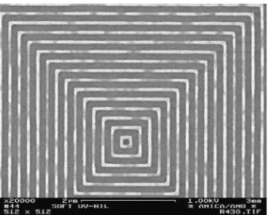
Figure 8: SEM micrographs illustrating high resolution Soft UV based Nanoimprint: 60nm lines closed to quadrates. [Courtesy of AMICA, AMO GmbH, Aachen]
Figure 8 illustrates the high resolution of the Soft UV based Nanoimprint process, where on the top 100nm lines and on the bottom 60nm lines closed to quadrates are shown.
4 CONCLUSION
There are no physical limitations encountered with imprinting techniques for fully replicated structures, in the sub-10nm range. The real challenge for the technique is its utilisation for dense structured full wafer imprints up to 200mm.
5 REFERENCES
[1] S.Y. Chou, P.R. Krauss, W. Zhang, L. Guo, L. Zhuang, “Sub-10 nm Imprint Lithography and Applications”, Journal of Vacuum Science and Technology B 15 (1997), 2897
[2] Perret, C.; Gourgon, C.; Lazzarino, F.; Tallal, J.; Landis, S.; Pelzer, R. 2003. Characterization of 8 Inch Wafers Printed by Nonoimprint Lithography. Proceedings of MNE Cambridge.
[3] Scheer, H.-C. ; Glinsner, T.; Wissen, M.; Pelzer, R. 2004. Nanostructuring of polymers by Hot Embossing Lithography. Proceedings of SPIE Microlithography 2004.
[4] Bender, M.; Plachetka, U.; Ran, J.; Fuchs, A.; Vratzov, B.; Kurz, H.; Glinsner, T.; Lindner, F.; 2004. High resolution lithogrpahy with PDMS-molds. EIPBN 2004.
![Figure 3: Uniformity control of imprints across 200mm wafers by measuring the residual thickness h r [Figure Courtesy of CNRS-LTM and CEA-LETI]](https://thumb-eu.123doks.com/thumbv2/123doknet/13038391.382259/4.892.472.758.157.364/figure-uniformity-control-imprints-measuring-residual-thickness-courtesy.webp)
![Risiko- & [und] Schutzfaktoren der psychischen Gesundheit humanitärer Einsatzhelfer : eine systematische Literaturübersicht](data:image/gif;base64,R0lGODlhAQABAIAAAP///wAAACH5BAEAAAAALAAAAAABAAEAAAICRAEAOw==)