HAL Id: hal-01736066
https://hal.archives-ouvertes.fr/hal-01736066
Submitted on 23 Mar 2018
HAL is a multi-disciplinary open access
archive for the deposit and dissemination of
sci-entific research documents, whether they are
pub-lished or not. The documents may come from
teaching and research institutions in France or
abroad, or from public or private research centers.
L’archive ouverte pluridisciplinaire HAL, est
destinée au dépôt et à la diffusion de documents
scientifiques de niveau recherche, publiés ou non,
émanant des établissements d’enseignement et de
recherche français ou étrangers, des laboratoires
publics ou privés.
Wet oxidation of nitride layer implanted with low-energy
Si ions for improved oxide-nitride-oxide memory stacks
V. Ioannou-Sougleridis, P. Dimitrakis, V.Em. Vamvakas, P. Normand,
Caroline Bonafos, Sylvie Schamm-Chardon, Nikolay Cherkashin, Gérard
Benassayag, M. Perego, M. Fanciulli
To cite this version:
V. Ioannou-Sougleridis, P. Dimitrakis, V.Em. Vamvakas, P. Normand, Caroline Bonafos, et al..
Wet oxidation of nitride layer implanted with low-energy Si ions for improved oxide-nitride-oxide
memory stacks. Applied Physics Letters, American Institute of Physics, 2007, 90 (26), pp.263513.
�10.1063/1.2752769�. �hal-01736066�
Wet oxidation of nitride layer implanted with low-energy Si ions for improved
oxide-nitride-oxide memory stacks
V. Ioannou-Sougleridis, P. Dimitrakis, V. Em. Vamvakas, P. Normand, C. Bonafos, S. Schamm, N. Cherkashin, G. Ben Assayag, M. Perego, and M. Fanciulli
Citation: Appl. Phys. Lett. 90, 263513 (2007); doi: 10.1063/1.2752769 View online: https://doi.org/10.1063/1.2752769
View Table of Contents: http://aip.scitation.org/toc/apl/90/26
Published by the American Institute of Physics
Articles you may be interested in
Thermal oxidation of silicon nitride and silicon oxynitride films
Journal of Vacuum Science & Technology B: Microelectronics Processing and Phenomena 7, 455 (1989); 10.1116/1.584769
Wet oxidation of nitride layer implanted with low-energy Si ions
for improved oxide-nitride-oxide memory stacks
V. Ioannou-Sougleridis,a兲 P. Dimitrakis, V. Em. Vamvakas, and P. Normand
Institute of Microelectronics, NCSR “Demokritos,” 153 10 Aghia Paraskevi, Greece
C. Bonafos, S. Schamm, N. Cherkashin, and G. Ben Assayag
CEMES-CNRS, 29 rue J. Marvig, 31055 Toulouse, France
M. Perego and M. Fanciulli
MDM CNR-INFM, via c. Olivetti 2, Agrate Brianza, 20041 Milano, Italy
共Received 23 March 2007; accepted 6 June 2007; published online 29 June 2007兲
An alternative method for the formation of the top oxide in oxide-nitride-oxide dielectric stacks is proposed. This method combines low-energy 共1 keV兲 silicon ion implantation into a thin nitride-oxide stack and subsequent low-temperature wet oxidation 共850 °C for 15 min兲. Transmission electron microscopy shows that for an implanted dose of 1.5⫻1016 Si cm−2, an 8-nm-thick silicon oxide layer develops on the surface of the nitride-oxide stack. Time of flight secondary ion mass spectrometry reveals: 共1兲 transformation of the implanted silicon nitride to an oxygen-rich-silicon nitride layer and 共2兲 pilling up of nitrogen atoms at the bottom silicon/ oxide-substrate interface. The resulting oxide-nitride-oxide stack exhibits strong charge storage effects and excellent charge retention properties leading to a 1.5 V, 10 yr extrapolated memory window at 125 ° C. These results suggest that the proposed fabrication route may lead to gate dielectric stacks of substantial potential impact for mainstream nitride-based memory devices. © 2007 American Institute of Physics.关DOI:10.1063/1.2752769兴
Nitride-based memory technology has the potential to fulfill the stringent requirements of nonvolatile memory cell downscaling.1This technology exploits the presence of dis-crete charge storage nodes in the form of deep traps distrib-uted in nitride materials. Due to its promising in terms of scalability, the conventional polycrystalline silicon/oxide/ nitride/oxide/silicon memory cell has regained a lot of atten-tion nowadays.2,3
Typical fabrication of the oxide/nitride/oxide 共ONO兲 stack consists in the growth of a thin SiO2 layer on a Si
substrate and subsequent deposition of a Si3N4layer. The top
silicon oxide is obtained by either deposition techniques or high temperature wet oxidation4,5 of the Si3N4 layer. The
latter approach has two main advantages. First, a thermal top oxide exhibits better insulating properties compared to a de-posited oxide. Second, during the oxidation step a silicon oxynitride transition layer forms between the top oxide and the remaining silicon nitride, containing a high density of traps. This layer can efficiently accommodate a larger pro-portion of trapped carriers as compared to that of stoichio-metric or Si-rich nitride.6However, fabrication of functional thermal blocking oxides requires high oxidation tempera-tures 共typically within the 1000 °C range7兲. For deep-submicron integration purposes, it is important to explore alternative technological routes that could lead to the forma-tion of a thermal top oxide at lower oxidaforma-tion temperatures. In this work a method for the formation of the top oxide in ONO stacks is proposed. This method is based on low-energy Si ion implantation into oxide-nitride共ON兲 structures followed by low-temperature wet oxidation. The structural and chemical properties as well as the memory performance
of the resulting ONO stacks are reported and compared to those of unimplanted ONO stacks.
SiO2and Si3N4stacks were first formed on a 4 in. n-type
共100兲 Si wafer. The oxide layer 共referred as tunnel or bottom oxide兲 was grown by dry oxidation at 850 °C to a thickness of 2.8 nm. The Si3N4 layer 6 nm thick was deposited by
low-pressure chemical vapor deposition共LPCVD兲 at 800 °C using a mixture of dichlorosilane 共SiH2Cl2兲 and ammonia
gasses 共NH3兲. Subsequently, the wafer was cut in to four pieces referred hereafter as samples II and C1–C3. Sample II was implanted with 1 keV Si ions to a dose of 1.5 ⫻1016cm−2. Si implantation using accelerating energy as
low as 1 keV allows for the introduction of Si atoms with a distribution confined in the nitride layer. Monte Carlo simu-lations using theTRIMcode and energy-filtered transmission electron microscopy 共TEM兲 analysis of high-temperature thermally annealed samples in N2, indicate that the peak of
the implanted profile is about 2.2 nm from the Si3N4
surface.8 In addition to Si enrichment of the implanted ni-tride materials, the implantation process produces a variety of defects such as vacancies, recoil N and Si atoms, and broken bonds that increase the density of reaction sites and thereby reduce the activation energy for oxidation. TRIM
depth distributions of vacancies and recoil atoms exhibit a projected range of about 1.6 nm from the free nitride inter-face with tails extending up to the middle region of the tun-nel oxide. WhileTRIM information on ion and defect distri-butions should be cautiously considered, especially in the case of low-energy high-dose ion implantation into thin di-electrics where a number of parameters9,10 共e.g., ion beam mixing, surface sputtering, and target swelling兲 contribute to the physicochemical changes of the target, one can assumed that the implantation process affects both the nitride layer and part of the tunnel oxide of sample II. Following the
a兲Author to whom correspondence should be addressed; electronic mail: v.ioannou@imel.demokritos.gr
APPLIED PHYSICS LETTERS 90, 263513共2007兲
implantation step, sample II was thermally oxidized in wet ambient at 850 ° C for 15 min to produce the top control oxide and further thermally annealed at 950 ° C in N2. The three control samples C1–C3 start with the non-Si-implanted ON stacks. Samples C1 and C2 consist of the dielectric stacks produced without and with the above wet oxidation step, respectively. Sample C3 refers to ONO stacks with 8-nm-thick top oxide produced by LPCVD at 700 ° C using tetraethylorthosilane and subsequently, thermally annealed at 950 ° C in N2. The structural and chemical characteristics of
the produced ONO stacks were investigated by TEM and time of flight secondary ion mass spectroscopy共ToF-SIMS兲. Finally, generic metal-ONO-semiconductor 共MONOS兲 Al gate capacitors were fabricated to study the electrical prop-erties and memory performance of the ONO stacks.
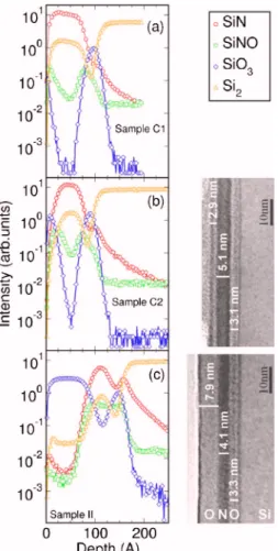
The effect of wet oxidation on the control and implanted ON structures was examined by cross-sectional TEM in de-focused bright field conditions. The method for distance measurements on such images is given in Ref.9, with error bars of ±0.5 nm. Wet oxidation of the control sample C2 forms a thin oxide layer共mean thickness of 2.9 nm兲 on top of the nitride layer, while the remaining nitride mean thick-ness is 5.1 nm关see Fig.1共b兲兴 and the thickness of the bottom oxide is around 3.1 nm. The ONO stack of sample C2 ex-hibits almost identical tunnel and top oxide thicknesses. On the contrary, the Si implanted and wet oxidized ON structure 共sample II兲 关Fig.1共c兲兴 presents an 8-nm-thick oxide on top of the remaining nitride layer共4.1 nm thick兲 and a bottom oxide
with a mean thickness of 3.3 nm. In addition, the interface of the top oxide with the nitride layer is flat and parallel to the bottom oxide-substrate interface indicating that the oxidation front is uniform.
Depth profile chemical compositions of the samples were obtained by ToF-SIMS. Sputtering was performed by Cs+ ions at 0.5 keV energy and 34 nA beam current. The analysis was made in negative polarity, using Ga+at 25 keV
energy and a current of 1.1 pA. Figure1shows the signals of the SiN, SiON, SiO3, and Si2 secondary ions. These signals
are related to the presence of Si nitride共SiN and Si2兲, silicon
dioxide 共SiO3兲, and silicon oxynitride 共SiON, SiN兲. Depth
scale calibration was performed using a SiO2film of known
thickness as a reference and assuming a constant sputter ve-locity throughout the ONO stack. The extracted layer thick-nesses are in agreement with TEM analysis. In the case of the unoxidized ON stack共C1兲, 关Fig.1共a兲兴, the presence of a double layer structure is detected. For the oxidized ON sample共C2兲 关Fig.1共b兲兴, the SiO3and SiON signals reveal a
surface oxide layer on top of the remaining nitride.
In the case of sample II 关Fig. 1共c兲兴, SiO3 signal shows
the formation of a thick silicon oxide layer. In comparison to sample C2, the SiON signal intensity is higher in the bulk of the nitride layer and extends down to the Si substrate. This indicates non-negligible oxygen content in the remaining ni-tride layer and the presence of nitrogen within the tunnel oxide. Moreover, in sample II, the SiN signal exhibits an intense peak at the tunnel oxide/Si-substrate interface with a long tail extending into the Si substrate. The tail is due to a well-known artifact related to mixing phenomena occurring during the sputtering process. The peak at the tunnel oxide/ Si-substrate interface indicates migration of nitrogen atoms toward the Si substrate during the implantation and oxidation processes.
Figure 2 shows typical high-frequency 共1 MHz兲 C-V characteristics of the ONO structures under study. The mea-surements were performed in the low-field regime to avoid charge injection and trapping effects. The extracted equiva-lent oxide thickness of samples II and C2, 14.2 and 8.5 nm, respectively, confirm TEM and ToF-SIMS results regarding the enhanced oxidation of Si-implanted ON stack. Compared to sample C3, the flatband voltages共VFB兲 of samples C2 and
II are about 1.0 and 0.3 V shifted to more positive values, respectively. These results are not only in accordance with the previous observations11 indicating that oxidation of ni-tride layer induces a positive shift of VFBbut also reveal that the latter effect is reduced for oxidized Si-implanted nitride
FIG. 1.共Color online兲 ToF-SIMS depth profiles of 共a兲 unoxidized 共sample C1兲, 共b兲 wet oxidized 共sample C2兲, and 共c兲 Si implanted and wet oxidized 共sample II兲 ON stacks. Defocused bright field cross-sectional TEM images are shown for samples C2 and II.
FIG. 2. Typical high-frequency C-V characteristics of MONOS capacitors from samples C2, C3, and II.
material. In our case, the origin of this effect is probably due to negatively charged defects such as the nitrogen vacancy with attached hydrogen atom.12
Memory performance of sample II MONOS devices un-der write/erase pulsed operation is shown in Fig.3. Single write共positive兲 and erase 共negative兲 pulses were applied af-ter setting the devices in near-saturation erase and write states, respectively. Clear saturation is detected in the 10 and 100 ms erasing regimes. It is believed that such saturation arises from the competitive effects of substrate hole injection and gate electron injection. Memory windows as large as 5.7 V can be obtained for 100 ms, +11/ −10 V and 10 ms, +12/ −11 V write/erase pulses, respectively. It should be mentioned that the ONO stack with deposited top oxide 共sample C3兲 exhibits no hole injection under erasing condi-tions and smaller VFBshifts in the write regime 共e.g., 4.1 V
for 100 ms +11 V兲. The absence of hole injection for sample C3 is due to the thick bottom dry oxide used in the present experiments. While the bottom oxide of sample II presents a larger physical thickness, its modified chemical composition allows for efficient erase operation.
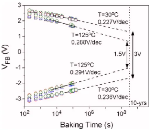
Figure 4 shows charge retention characteristics of sample II MONOS devices at 30 and 125 ° C. The capacitors were initially charged using 100 ms, −10 and +11 V pulses for the erase and write states, respectively. The flatband volt-age was monitored for waiting times as large as 105s. The
extracted charge 共electron兲 loss rate for the write state was 0.23 V / decade at 30 ° C and 0.29 V / decade at 125 ° C. In the case of the erase state, charge loss rates of 0.24 and 0.29 V / decade were found at 30 and 125 ° C, respectively. Long time extrapolation indicates 10 yr memory windows of about 3 and 1.5 V at 30 and 125 ° C, respectively.
In summary, it has been presented that a combination of low-energy silicon ion implantation into ON structures and
subsequent low-temperature wet oxidation provides an at-tractive technological route for the fabrication of ONO di-electric stacks. Such a route produces thick and reliable top oxides as well as transforms the nitride layer to silicon ox-ynitride materials. Both the write/erase and data retention characteristics obtained throughout the measurements per-formed so far suggest that the ONO stacks reported herein are attractive for the development of nitride storage memory cells.
1C. Y. Lu, T. C. Lu, and R. Liu, Proceedings of the 13th International Symposium on the Physical and Failure Analysis of Integrated Circuits 共IPFA兲, Singapore, July 2006, p. 18.
2M. H. White, Y. Wang, S. J. Wrazien, and Y. Zhao, Int. J. High Speed Electron. Syst. 16, 479共2006兲.
3R. van Schaijk, M. Slotboom, M. van Duuren, D. Dormans, N. Akil, R. Beurze, F. Neuilly, W. Baks, A. H. Miranda, and P. G. Tello, Solid-State Electron. 49, 1849共2006兲.
4L. U. T. Ogbuli and D. T. Jayne, J. Electrochem. Soc. 140, 759共1993兲. 5H. Du, R. E. Tressler, and K. E. Spear, J. Electrochem. Soc. 136, 3210
共1989兲.
6E. Suzuki, Y. Hayashi, K. Ishii, and T. Tsuchiya, Appl. Phys. Lett. 42, 608 共1982兲.
7M. Saraf, R. Edrei, R. Akhvlediani, Y. Roizin, R. Shima-Edelstein, and A. Hoffman, 24, 1716共2006兲.
8V. Ioannou-Sougleridis, P. Dimitrakis, V. Em. Vamvakas, P. Normand, C. Bonafos, S. Schamm, A. Mouti, G. Ben Assayag, and V. Paillard, Nanotechnology 18, 215204共2007兲.
9C. Bonafos, M. Carrada, N. Cherkashin, H. Coffin, D. Chassaing, G. Ben Assayag, A. Claverie, T. Muller, K. H. Heinig, M. Perego, M. Fanciulli, P. Dimitrakis, and P. Normand, J. Appl. Phys. 95, 5696共2004兲.
10P. Normand, E. Kapetanakis, P. Dimitrakis, D. Skarlatos, K. Beltsios, D. Tsoukalas, C. Bonafos, G. Ben Assayag, N. Cherkashin, A. Claverie, J. A. Van Den Berg, V. Soncini, A. Agarwal, M. Ammen, M. Perego, and M. Fanciulli, Nucl. Instrum. Methods Phys. Res. B 216, 228共2004兲. 11S. Y. Wang, H. T. Lue, E. K. Lai, L. W. Yang, J. Gong, K. C. Chen, K. Y.
Hsieh, J. Ku, and C. Y. Lu, Solid-State Electron. 50, 1171共2006兲. 12M. Petersen and Y. Roizin, Appl. Phys. Lett. 89, 053511共2006兲. FIG. 3. Write/erase characteristics of Si-implanted-nitride ONO capacitors
共sample II兲 for 10 and 100 ms pulse duration. FIG. 4. 共Color online兲 Charge retention characteristics of Si-implanted-nitride ONO capacitors共sample II兲 at 30 and 125 °C.