HAL Id: hal-01343422
https://hal.archives-ouvertes.fr/hal-01343422
Submitted on 8 Jul 2016
HAL is a multi-disciplinary open access archive for the deposit and dissemination of sci-entific research documents, whether they are pub-lished or not. The documents may come from teaching and research institutions in France or abroad, or from public or private research centers.
L’archive ouverte pluridisciplinaire HAL, est destinée au dépôt et à la diffusion de documents scientifiques de niveau recherche, publiés ou non, émanant des établissements d’enseignement et de recherche français ou étrangers, des laboratoires publics ou privés.
Generation-Recombination Defects In AlGaN/GaN
HEMT On SiC Substrate, Evidenced By Low Frequency
Noise Measurements And SIMS Characterization
Jean-Guy Tartarin, Geoffroy Soubercaze-Pun, Jean-Laurent Grondin, Laurent
Bary, Jaime Mimila-Arroyo, Jacques Chevallier
To cite this version:
Jean-Guy Tartarin, Geoffroy Soubercaze-Pun, Jean-Laurent Grondin, Laurent Bary, Jaime Mimila-Arroyo, et al.. Generation-Recombination Defects In AlGaN/GaN HEMT On SiC Substrate, Ev-idenced By Low Frequency Noise Measurements And SIMS Characterization. 19th International Conference on Noise and Fluctuations (ICNF 2007), Sep 2007, Tokyo, Japan. �10.1063/1.2759658�. �hal-01343422�
Generation-Recombination Defects In
AlGaN/GaN HEMT On SiC Substrate,
Evidenced By Low Frequency Noise
Measurements And SIMS Characterization
Jean-Guy Tartarin
+*, Geoffroy Soubercaze-Pun
+0, Jean-Laurent Grondin
+*,
Laurent Bary
+, Jaime Mimila-Arroyo
#, Jacques Chevallier
#+
LAAS-CNRS, 7 av. Colonel Roche, 31077 Toulouse cedex 4, France
*
University of Toulouse III, 118 rte de Narbonne, 31.062 Toulouse, France
0
Thales Alenia Space, 26 av. Champollion, BP 1187, 31.037Toulouse, France
#
LPSC, 1 place Aristide Briand, 92.195 Meudon, France
Abstract. Wide bandgap devices such as AlGaN/GaN High Electron Mobility Transistors (HEMT) grown on silicon carbide (SiC) substrate are investigated. Low frequency noise (LFN) measurements have been carried out to evaluate the structural perfection of dual gated HEMT devices featuring 0.25x2x75µm² gate area: generation-recombination (GR) processes are evidenced. Two sets of GR-bulges related respectively to AlGaN/GaN interface and quantum well are identified. Each GR-bulge is composed of two GR centers. The devices are then characterized in a temperature controlled oven, and these GR centers are extracted from LFN spectra versus temperature. Activation energies of the defects located at the AlGaN/GaN interface are measured at 0.38±0.05eV and 0.21±0.05eV using Arrhenius plots under saturated biasing conditions. Equivalent activation energies are extracted under ohmic biasing conditions. These results are compared with SIMS measurements, using the deuterium in diffusion condition as a probe to integrally explore the presence of defects throughout the AlGaN-GaN HEMT structure. Large concentrations of deuterium (more than 1020 D concentration per cm3) are measured at the AlGaN/GaN interface and in the 2DEG layer, thus proving the presence of numerous vacations at the AlGaN/GaN interface as well as in the 2DEG. From the confrontation with previously published results, the defects might be assigned to the nitrogen vacancy and to MgGa-VN complexes.
Keywords: trapping detrapping effects, Low frequency noise, SIMS, activation energy, GaN. PACS: 72.20.Jv, 72.70.+m, 72.80.Ey
ALGAN/GAN HEMT FOR LOW NOISE APPLICATIONS
Although GaN technologies were initially developed for solid state power amplifiers (SSPA), it has been recently demonstrated that AlGaN/GaN High Electron Mobility Transistor (HEMT) are also suitable for low noise applications such as low noise amplifiers (LNA) [1][2] and low phase noise oscillators [3]. Here, low frequency noise (LFN) measurements are used to identify the defects induced in AlGaN/GaN HEMT, impacting non-linear noise applications and reliability. LFN measurements on HEMT can be used to identify the defects, and thus improve both the technological process and the reliability of the devices.
Static Measurements And Low Frequency Noise Characterization
HEMT devices are grown by MOCVD on silicon carbide (SiC) substrate (TIGER process). High drain current (1A/mm), high transconductance (250mS/mm) and low gate leakage current (<0.1µA) as well as reduced contact (11Ω) and RON channel
resistances (25Ω) are measured, highlighting the good process maturity. The transition and maximum frequencies are measured respectively at 40 GHz and 100 GHz.
1E-20 1E-19 1E-18 1E-17 1E-16 1E-15 1E-14
1E+1 1E+2 1E+3 1E+4 1E+5
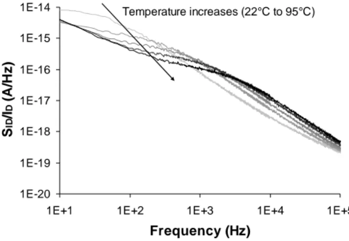
Frequency (Hz) S ID /I D (A /H z ) Temperature increases (22°C to 95°C)
FIGURE 1. normalized drain current spectral density spectra SID/ID versus frequency for different ambient temperatures (22°C<T<95°C). The device under test features 2x0.25x75µm² gate area. From LFN study, no cross-correlation is found between SID and SIG spectral
densities, and only SID spectra are considered next (fig. 1). LFN spectra are measured
in the range of 10 Hz – 100 kHz. The measurements are performed on packaged devices in a temperature controlled oven: SID features 1/f flicker noise contribution
with a generation recombination (GR) bulge composed by two Lorentzian’s noise sources. These two GRs are extracted using an accurate mathematical procedure.
Activation Energies Under Ohmic And Saturated Biasing Conditions
-1,5E-23 -5,0E-24 5,0E-24 1,5E-23 2,5E-23 3,5E-23
2,7E-03 2,9E-03 3,1E-03 3,3E-03
1000/T (K-1) kB .L n( T² / τc ) GR1 Ea=0.38± 0.05 eV GR2 Ea=0.21± 0.05 eV
FIGURE 2. Arrhenius plot for GR1 and GR2 trapping detrapping centers, for temperatures varying
A study at constant VGS=0V and VDS=6V (figure 1) for different ambient
temperature ranging from 22 K to 95 K is performed. The two G-Rs centers GR1 and GR2 contributing to the LFN bulge are extracted from each different spectrum. Figure 2 illustrates the Arrhenius plots for the trapping detrapping centers, and activation energies are found at 0.38±0.05 eV and at 0.21±0.05 eV respectively for GR1 and GR2 (τc represents the capture time constant of the trap, issued from the cutoff
frequency of the GR lorentzian’s noise source). Activation energies are extracted respectively at 0.39±0.05 eV and 0.29±0.05 eV respectively for GR1 and GR2 under ohmic biasing conditions. Thus we can suppose that the same defect is activated under linear and saturated operating modes.
SIMS CHARACTERIZATION ON DEUTERATED STRUCTURES
Secondary Ions Mass Spectrometry (SIMS) are also performed on AlGaN/GaN samples issued from the same wafer, without any metallization for the gate, drain or source accesses Hydrogen usually bonds to defects in semiconductors: Deuterium in-diffusion in the AlGaN-GaN HEMT structure has been already published [4]. The deuterium in diffusion conditions are optimized in order to use it as a probe to integrally explore the presence of defects throughout the AlGaN-GaN HEMT structure (AlGaN, interface and GaN layers). The in diffusion of deuterium in the AlGaN-GaN structure produces a profile composed of three parts, as shown in figure 3.
1.E+00 1.E+02 1.E+04 1.E+06 10 100 1000 10000 DEPTH (A) D CON C ENTRATI O N (c m -3) AS DEUTERATED RTA 800°C 180s DEUTERTED ( 30W, 460 C, 90 min) 1017 1019 1015 1021 AlGaN GaN Deuterated (30W, 460 C, 90 min) 1.E+00 1.E+02 1.E+04 1.E+06 10 100 1000 10000 DEPTH (A) D CON C ENTRATI O N (c m -3) AS DEUTERATED RTA 800°C 180s DEUTERTED ( 30W, 460 C, 90 min) 1017 1019 1015 1021 AlGaN GaN Deuterated (30W, 460 C, 90 min)
FIGURE 3. Deuteration concentration versus sample depth, using SIMS technique.
The first part, with a deuterium concentration in the middle 1020 cm-3 reaching a depth identical to the AlGaN thickness and displaying a concentration maximum at the interface, shows the deuterium trapped by defects in this layer and at the interface. The second part, located at the GaN side of the AlGaN-GaN interface, 30 to 80 nm in figure 3, corresponds to deuterium trapped by the two dimension electron gas, as there deuterium behaves like an acceptor becoming H-, whose activation energy to diffuse is quite high ~3.4 eV (larger than our activation energies). The third part of the deuterium profile, that covers the whole thickness of the GaN layer, is a long deuterium plateau at a concentration close to 1017 cm-3 which corresponds to deuterium complexed with some acceptor impurity.
DISCUSSIONS
HEMT device is based on majority carriers: the noise sources are constituted by charges at energy levels in the forbidden band gap that should interact with the conduction band. From our LFN measurements two trapping centers located at 0.21 ± 0.05 and 0.38 ± 0.05 eV have been extracted. On the other hand deep level transient spectroscopy studies have show the presence of levels located at 0.2, 0.21 [5] and 0.44 eV [6] from the conduction band, with capture cross sections of 8.4x10⁻¹⁷ cm-2, 1.6x10⁻¹⁴ cm-2 and 1.3x10⁻¹⁵ cm-2, respectively. The level located at 0.21 eV with capture cross section of 1.6x10⁻¹⁴ cm-2 has been assigned to the nitrogen vacancy, VN
[5]. From the behavior shown by the extracted levels through our LFN measurements it can be concluded that we are dealing with levels displaying similar capture cross sections and concentrations. Then, from the two levels around 0.2 eV, the one featuring a capture cross section of 8.4x10⁻¹⁷ cm-2 can be ruled out. Thus, we conclude that in our case the LFN extracted level at 0.21 ± 0.05 might be assigned to the nitrogen vacancy. For the 0.38 ± 0.05 eV level, it has been reported that the acceptor MgGa paired to the nitrogen vacancy, MgGa-VN introduces a donor level at 0.43 eV [7].
Given the high temperatures used to grow the non-intentionally doped GaN (location of the 2DEG) high nitrogen vacancy concentration can be expected close to 1017 cm-3 according to our SIMS measurements. Some nitrogen vacancies remain isolated yielding the level discussed above and some might get paired forming complex with residual acceptor MgGa whose presence seems to be confirmed by the stable deuterium
plateau obtained, as well, by our deuteration and SIMS experiments.
ACKNOWLEDGMENTS
This work is supported by the French Ministry of Research under RNRT’s financial project (ANDRO). The authors specially want to thank TIGER (Thales Research Technology and IEMN CNRS laboratory) for providing the devices of this study.
REFERENCES
1. J.G. Tartarin et al.“Low frequency and linear high frequency noise performances of AlGaN/GaN grown on SiC substrate,” Gallium Arsenide and Other Semiconductor Application Symposium, October 2005, pp 277-280.
2. D. Krausse et al.“Robust GaN HEMT Low-noise amplifier MMIC for X-band applications”, Gallium Arsenide and Other Semiconductor Application Symposium, October 2004, pp 71-74. 3. G. Soubercaze-Pun et al.“Design of a X-band GaN oscillator: from the low frequency noise device
characterization and large signal modeling to circuit design” International Microwave Symposium, Miccrowave Theory and Technique MTT’S 06, San Francisco, USA, June 2006, pp. 747-750. 4. J. Chevallier et al., “Solid State Phenomena”, Vols. 85-86, 2002 pp. 203.
5. Z.Q. Fang et al., “Deep centers in n-GaN grown by reactive molecular beam epitaxy”, Applied Physics Letters, Vol. 72, N° 18, 4 May 1998, pp. 2277-2279.
6. S. Danylyunk, “Design and development of radiation-resistant and low-noise semiconductor transistors for applications in high frequency communication systems”, Institut fur Shrichten und Grenzflacher, ISSN 0944-2952, December 2004.
7. U. Kaufmann, M. Kunzer, M. Maier, H. Obloh, A. Ramakrishnan, B. Santic, and P. Schlotter, Appl. Phys. Lett. 72, 1326 (1998).