HAL Id: tel-01406363
https://tel.archives-ouvertes.fr/tel-01406363
Submitted on 1 Dec 2016
HAL is a multi-disciplinary open access archive for the deposit and dissemination of sci-entific research documents, whether they are pub-lished or not. The documents may come from teaching and research institutions in France or abroad, or from public or private research centers.
L’archive ouverte pluridisciplinaire HAL, est destinée au dépôt et à la diffusion de documents scientifiques de niveau recherche, publiés ou non, émanant des établissements d’enseignement et de recherche français ou étrangers, des laboratoires publics ou privés.
Zhixiong Cao
To cite this version:
Zhixiong Cao. Silver nanoprisms in plasmonic organic solar cells. Micro and nanotechnolo-gies/Microelectronics. Ecole Centrale Marseille, 2014. English. �NNT : 2014ECDM0015�. �tel-01406363�
École Doctorale ED 353 - Sciences Physiques pour l’Ingénieur Préparée au laboratoire IM2NP, UMR-CNRS 7334, équipe Opto-PV
THÈSE DE DOCTORAT
pour obtenir le grade de
DOCTEUR de l’ÉCOLE CENTRALE de MARSEILLE
Discipline : Micro Nano électronique
TITRE DE LA THÈSE : Silver nanoprisms in plasmonic
organic solar cells
Par
CAO Zhixiong
Directeur de thèse : ESCOUBAS Ludovic
Co-directrice de thèse : CHEN Zhuoying
Soutenue le 15 Décembre 2014 devant le jury composé de :
LEQUEUX Nicolas Prof de l’ESPCI, Paris Rapporteur
VIGNAU Laurence Prof de l’Université de Bordeaux I, Bordeaux Rapporteur RATIER Bernard Prof de l’Université de Limoges, Limoges Examinateur ESCOUBAS Ludovic Prof de l’Université d'Aix-Marseille, Marseille Directeur de thèse CHEN Zhuoying Chargé de recherche au CNRS, ESPCI, Paris Co-directrice de thèse
First of all, this thesis is a project of collaboration between Chinese Scholarship Council (CSC) and Ecole Centrale groups of Lille, Nantes, Lyon, Paris, and Marseille. I appreciate the CSC and Ecole Centrale de Marseille, as well as the OPTO-PV group, IM2NP (Institut Matériaux Microélectronique Nanosciences de Provence), Aix-Marseille University and CNRS 7334 & 8213 for financial support.
I would like also thank my thesis committee, which includes Prof. VIGNAU Laurence, LEQUEUX Nicolas and RATIER Bernard.
Particularly, I really appreciate my thesis supervisors, Dr. CHEN Zhuoying and Prof. ESCOUBAS Ludovic. They helped me so much: they gave me many advices on experiments, took a lot of time to correct all my thesis and paper in detail…. Anyway, without their helps, tolerance and encouragement, I could probably not finish my thesis. Thank you, my supervisors!
I also want to thank my dear brother, Mr. CAO Chaoqun. Without his sacrifice and financial support, I could not finish my studies in high school and in university, and so that I would not finish my thesis. I would like to say: you are great, my brother!
I also acknowledge the technicians, M. FAURE Yves, WARCHOL François and COMBES Alain, FIORIDO Tomas, as well as mu colleagues and friends: PASQUINELLI Marcel, BARAKEL Damien, BRISSONNEAU Vincent, BERENGUIER Baptiste, BOU Adrien, BRUCKNER Jean-Baptiste, WOOD Thomas, ZHU Mingxuan and VEDRAINE Sylvain for their helps. I appreciate Dr. XU Xiangzhen (ESPCI, Paris), the courtesy of Concept Scientific Instruments and ScienTec Company for their helps in characterizations.
In the end, I would like to thank all of my friends and colleagues appeared in my life in France. It was a joyful and colorful life staying in France with them.
i
Table of Contents
Table of Contents ... i
Table of Figures ... vii
List of Tables ... xv
General introduction ... 1
Chapter I ... 3
Introduction and Background Knowledge ... 3
1.1. Introduction ... 3
1.2. State-of-art of photovoltaics ... 3
1.2.1. History and development of photovoltaics ... 3
1.2.2. Development of organic solar cells ... 6
1.3. Basic knowledge of organic solar cells ... 7
1.3.1. Organic semiconductors and their applications in solar cells ... 7
1.3.2. The electronic structure of conjugated polymers ... 7
1.3.3. Excitons and polarons in organic semiconductors ... 10
1.3.4. Photo-conversion process ... 11
1.3.4.1. Absorption of photons and generation of excitons ... 11
1.3.4.2. Diffusion of excitons ... 14
1.3.4.3. Dissociation of excitons ... 15
1.3.4.4. Transport of charge carriers ... 16
1.3.4.5. Extraction of charges ... 17
1.3.5. Architectures of organic solar cells ... 18
1.3.5.1. General architecture of organic solar cells ... 18
1.3.5.2. Single layer cells ... 19
ii
1.3.5.4. Bulk heterojunction cells ... 19
1.3.5.5. Tandem solar cells ... 19
1.4. Organic bulk heterojunction solar cells using polymers and small molecules ... 20
1.4.1. Hole extraction layer: PEDOT:PSS ... 20
1.4.2. Bulk heterojunction ... 22
1.4.2.1. Donor material: P3HT ... 22
1.4.2.2. Acceptor material: PCBM ... 25
1.4.2.3. P3HT:PCBM film ... 26
1.4.3. Photovoltaic Characteristics of organic solar cells ... 27
1.4.3.1. Current-voltage response and efficiency ... 27
1.4.3.2. Performance-limiting factors ... 29
1.5. Plasmonic organic solar cells ... 32
1.5.1. Plasmons ... 33
1.5.1.1. Bulk plasmons ... 33
1.5.1.2. Surface plasmons on planar metal-dielectric interfaces ... 34
1.5.1.3. Localized surface plasmons in metallic nanoparticles ... 35
1.5.2. Organic solar cells utilizing localized surface plasmons ... 42
1.5.2.1. Mechanisms of light absorption enhanced by localized surface plasmons .. 42
1.5.2.2. Plasmonic organic solar cells ... 43
1.6. Conclusions ... 45
Chapter II ... 47
Experimental methods and techniques ... 47
2.1. Materials ... 47
2.2. Film and photovoltaic device preparation ... 48
2.2.1. General preparation technique for thin films: Spin-coating ... 48
iii
2.2.2.1. General preparation procedure for films on glass substrate or ITO-coated
substrate and for photovoltaic devices ... 49
2.2.2.2. Preparation of sample PEDOT:PSS films and OSCs for optimization of PEDOT:PSS layer by post-deposition thermal annealing ... 52
2.2.2.3. Preparation of sample PEDOT:PSS films and OSCs for optimization of PEDOT:PSS layer by adding glycerol ... 52
2.2.2.4. Sample preparation for optimization of photoactive layer ... 52
2.2.2.5. Sample preparation for plasmonic OSCs using Ag NPSMs in PEDOT:PSS layer 53 2.2.2.6. Sample preparation for plasmonic OSCs using Ag NPSMs and glycerol in PEDOT:PSS layer ... 53
2.3. Characterization Methods ... 54
2.3.1. Characterization technique for Ag nanoparticles and solutions ... 54
2.3.1.1. UV-visible absorption for solutions ... 54
2.3.1.2. X-ray Diffraction ... 55
2.3.1.3. Transmission electron microscopy ... 55
2.3.2. Characterization techniques for films ... 56
2.3.2.1. Thickness determination ... 56
2.3.2.2. Integrating sphere photometer for films ... 56
2.3.2.3. Goniophotometry ... 58
2.3.2.4. Atomic Force Microscopy and conductive Atomic Force Microscopy ... 60
2.3.2.5. Four point probe measurement ... 62
2.3.3. Characterization techniques for solar cells ... 63
2.3.3.1. Current-Voltage Characterization ... 63
2.3.3.2. External quantum efficiency ... 63
2.4. Conclusion ... 65
iv
Structural, optical and electrical properties of PEDOT:PSS thin films doped with silver
nanoprisms ... 67
3.1. Introduction ... 67
3.2. Ag NPSM synthesis and characterizations ... 68
3.2.1. Ag NPSMs synthesis ... 69
3.2.2. Characterizations of Ag NPSMs ... 70
3.3. Hybrid PEDOT:PSS-Ag NPSM solutions and films ... 74
3.3.1. Preparation of hybrid PEDOT:PSS-Ag NPSM solutions and films ... 74
3.3.2. Characterizations of hybrid PEDOT:PSS films ... 75
3.3.2.1. Absorptance ... 75
3.3.2.2. Bidirectional Reflectance Distribution Function (BRDF) ... 76
3.3.2.3. Surface profile and electrical conductivity ... 77
3.4. Conclusions ... 79
Chapter IV ... 81
Plasmonic organic solar cells using silver nanoprisms ... 81
4.1. Optimization of regular P3HT:PCBM solar cells ... 81
4.1.1. Introduction ... 81
4.1.2. Optimization of PEDOT:PSS layer ... 81
4.1.2.1. Thermal annealing of PEDOT:PSS films... 81
4.1.2.2. Glycerol modified PEDOT:PSS ... 86
4.1.3. Optimization of photoactive layer ... 87
4.1.3.1. Thermal annealing ... 89
4.1.3.2. Solvent annealing and additive for photoactive layer ... 90
4.2. Studies of plasmonic solar cells composing silver nanoprisms in PEDOT:PSS... 93
4.2.1. Introduction ... 93
4.2.2. plasmonic solar cells composing silver nanoprisms in PEDOT:PSS ... 93
v
4.2.2.2. Characterization and discussion ... 93
4.2.3. Plasmonic OSCs composing Ag NPSMs and glycerol in PEDOT:PSS layer 100 4.2.3.1. Introduction ... 100
4.2.3.2. Characterization and discussion ... 101
4.3. Conclusions ... 103
General conclusions and prospective ... 105
General conclusions ... 105
Prospective ... 107
Appendix I Ag Nanospheres Synthesis ... 109
Appendix II Ag nanoprisms synthesis by one-step thermal reduction ... 111
Appendix III Photovoltaic characteristics of PTB7:PC70BM organic solar cell ... 113
Appendix IV Phase transfer of Ag nanoprisms from aqueous solution into organic solvents 115 Appendix V Plasmonic organic solar cells using Ag nanoprisms in active layer ... 121
vii
Table of Figures
FIGURE 1.1EVOLUTION OF SOLAR CELLS’ POWER CONVERSION EFFICIENCY RECORD FOR ALL TYPES OF PHOTOVOLTAICS [10] ... 5 FIGURE 1.2EVOLUTION OF POWER CONVERSION EFFICIENCY OF ORGANIC SOLAR CELLS IN THE
LAST DECADE ... 6 FIGURE 1.3SOME CONJUGATED POLYMERS INVESTIGATED IN PV CELLS.TOP:POLYETHYLENE,
POLY(P-PHENYLENE VINYLENE)(PPV), POLY(2-METHOXY-5-(20-ETHYL
-HEXYLOXY)-1,4-PHENYLVINYLENE)(MEH-PPV), POLY(3-HEXYLTHIOPHENE)(P3HT).
BOTTOM:PCPDTBT,PTB7. ... 8 FIGURE 1.4STRUCTURE, ELECTRON CLOUD DISTRIBUTION, BONDING Π ORBITAL TO THE
ANTI-BONDING Π* ORBITAL OF ETHYLENE ... 8
FIGURE 1.5EVOLUTION OF Π MOLECULAR ORBITALS IN CONJUGATED POLYMERS WITH
INCREASING CONJUGATION LENGTH ... 9
FIGURE 1.6POLARONIC (POSITIVE AND NEGATIVE POLARON) AND EXCITONIC (EXCITON) ENERGY LEVELS AND THE ASSOCIATED SUB-BANDGAP TRANSITIONS.TRANSITIONS (E2&E4) IN DASH-LINE ARE SYMMETRICALLY DISALLOWED. ... 11
FIGURE 1.7ILLUSTRATION OF AM0,AM1.5 AND AMX.NOTE THAT AT THE ZENITH, THE SUN IS DIRECTLY OVERHEAD AND Θ =0;AM0 IS THE SOLAR SPECTRUM JUST ABOVE THE
ATMOSPHERE AT Θ =0;AM1.5 IS THE SOLAR SPECTRUM WITH AN INCIDENT ANGLE OF 48.2° FROM THE ZENITH;X=1/COSΘ. ... 12 FIGURE 1.8THE SIX STEPS OF PHOTO-CONVERSION PROCESS IN BULK HETEROJUNCTION CELLS13 FIGURE 1.9AM0 AND AM1.5 SOLAR SPECTRA [41] AND ABSORBANCE OF P3HT ... 14 FIGURE 1.10JABLONSKI DIAGRAM OF LIGHT ABSORPTION PROCESS IN CONJUGATED POLYMERS
... 14 FIGURE 1.11FÖRSTER AND DEXTER DIFFUSION MECHNAISMS FOR SINGLET AND TRIPLET
EXCITONS, RESPECTIVELY (ADOPTED FROM [42]) ... 15 FIGURE 1.12SCHEMATIC JABLONSKI DIAGRAM DESCRIBING THE PHOTO-INDUCED
CHARGE-CARRIER FORMATION MECHANISM IN AN ORGANIC SOLAR CELL:S0 IS THE SINGLET GROUND STATE OF THE DONOR OR THE ACCEPTOR,S1 AND T1 THE fiRST SINGLET AND TRIPLET EXCITED STATE, RESPECTIVELY; THE LEFT SUPERIOR 1 AND 3 DENOTES THE SINGLET AND
viii
TRIPLET EXCITONS; SYMBOL * DENOTES THE EXCITED STATE;+ AND – REPRESENT THE
POSITIVE AND NEGATIVE CHARGE, RESPECTIVELY.(ADOPTED FROM REFERENCE [40]) ... 16
FIGURE 1.13CHARGE GENERATION PROCESS IN ORGANIC SOLAR CELLS.LEFT: INDIRECT FORMATION OF CT EXCITON; RIGHT: DIRECT FORMATION OF CT EXCITON BY PHOTON ABSORPTION (ADOPTED FROM REFERENCE [44]) ... 16
FIGURE 1.14SCHEMATIC OF METAL-SEMICONDUCTOR CONTACTS.NOTE THAT THE BLACK DOTS AT THE METAL-SEMICONDUCTOR INTERFACE REPRESENT ELECTRONS AND CIRCLES REPRESENT HOLES;EV IS THE ENERGY LEVEL OF THE TOP OF THE VALANCE BAND AND EC IS THE ENERGY LEVEL OF THE BOTTOM OF THE CONDUCTION BAND;EVACUUM IS THE ENERGY LEVEL OF VACUUM WHILE EF IS THE FERMI LEVEL. ... 17
FIGURE 1.15GENERAL ARCHITECTURE OF ORGANIC SOLAR CELL:HEL DENOTES THE HOLE EXTRACTION LAYER, AND EEL THE ELECTRON EXTRACTION LAYER. ... 20
FIGURE 1.16STRUCTURES OF PEDOT AND PSS, ADOPTED FROM REFERENCE [53] ... 21
FIGURE 1.17SCHEMATIC OF PEDOT:PSS COMPLEX, ADOPTED FROM REFERENCE [55] ... 21
FIGURE 1.18CHEMICAL STRUCTURES OF POLY(3-HEXYLTHIOPHENE-2,5-DIYL) ... 23
FIGURE 1.19POSSIBLE COUPLINGS OF TWO 3-HEXYLTHIOPHENE MONOMERS FOR P3HT ... 23
FIGURE 1.20INTERMOLECULAR INTERACTIONS OF SIDE-CHAINS OF LAMELLAR STRUCTURES OF REGIOREGULAR P3HT: A AND B ARE THE LATTICE CONSTANTS AND A-AXIS IS PERPENDICULAR TO SUBSTRATE WHILE B-AXIS PARALLEL TO SUBSTRATE (REPRINTED FROM REFERENCE [93]) ... 24
FIGURE 1.21AFM IMAGES OF (A) CRYSTALLINE ROD-LIKE MORPHOLOGY OF LOW MN P3HT(3.2 KDA) AND (B) NODULE STRUCTURE FOR HIGH MN P3HT FILM (31 KDA).(C) SCHEMATIC OF BADLY CONNECTED ROD-LIKE CRYSTALLINE FOR LOW MN P3HT AND (D) INCREASED NETWORKING BETWEEN CRYSTALLINE DOMAINS FOR HIGH MN P3HT FILM (REPRINTED FROM [96] WITH PERMISSION OF THE ROYAL SOCIETY OF CHEMISTRY) ... 25
FIGURE 1.22STRUCTURES OF FULLERENE DERIVATIVES, FROM LEFT TO RIGHT:PC60BM, PC70BM AND PC84BM [98,113] ... 27
FIGURE 1.23P3HT:PCBM THICKNESS-DEPENDENT POWER CONVERSION EFFICIENCY [111,112] ... 27
ix
FIGURE 1.24CURRENT VERSUS APPLIED VOLTAGE OF A SOLAR CELL: THE RED CURVE IS OBTAINED FOR MEASUREMENT IN THE DARK AND THE BLACK CURVE IS THE RESULT OF
MEASUREMENT UNDER ILLUMINATION ... 28 FIGURE 1.25EFFECTS OF RS AND RSH ON FILL FACTOR,JSC AND VOC [116]. ... 32
FIGURE 1.26SCHEMATIC BAND DIAGRAM FOR THE NOBLE METALS [148]: INTER-BAND
TRANSITION BETWEEN D-BAND AND CONDUCTION BAND; INTRA-BAND TRANSITION WITHIN CONDUCTION BAND) ... 34 FIGURE 1.27SCHEMATIC OF CHARGE DISTRIBUTION AND ELECTROMAGNETIC FIELD OF SURFACE PLASMONS ... 35 FIGURE 1.28LOCALIZED SURFACE PLASMONS IN A METALLIC NANOPARTICLE ... 36 FIGURE 1.29FINITE-DIFFERENCE TIME-DOMAIN (FDTD) EXTINCTION SIMULATIONS OF AG
NANOPARTICLES WITH IDENTICAL VOLUME, TAKEN TO BE THAT OF A SPHERE WITH A RADIUS OF 50 NM (REPRINTED FROM [168],MATERIALS RESEARCH SOCIETY,MRSBULLETIN) .. 39
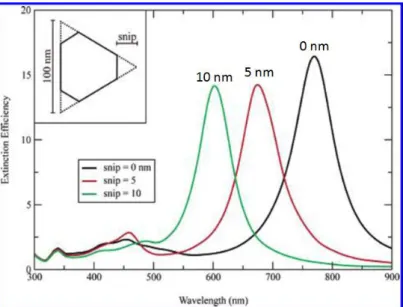
FIGURE 1.30DDA EXTINCTION SIMULATIONS OF TIP TRUNCATED TRIANGULAR PRISMS.INSET: THE SHAPE OF A SNIPPED PRISM.THE PRISM THICKNESS IS 16 NM.( REPRINTED FROM [169],
AMERICAN CHEMISTRY SOCIETY, THE JOURNAL OF PHYSICAL CHEMISTRY B). ... 39
FIGURE 1.31SIMULATIONS OF ELECTRIC-FIELD ENHANCEMENT CONTOURS EXTERNAL TO THE AG TRIANGULAR PRISM, LEFT IS IN-PLANE MAIN DIPOLE AND THE RIGHT IS IN-PLANE
QUADRUPOLE (REPRINTED FROM [169],AMERICAN CHEMISTRY SOCIETY, THE JOURNAL OF
PHYSICAL CHEMISTRY B) ... 40
FIGURE 1.32EXTINCTION SPECTRA OF A 2D ARRAY OF THE AU NANOPARTICLE PAIRS WITH THE INTERPARTICLE CENTER-TO-CENTER SPACING AS THE PARAMETER [182] ... 42
FIGURE 1.33DIFFERENT LIGHT TRAPPING MECHANISMS: LIGHT SCATTERING FROM LARGE DIAMETER (>50 NM) METAL NPS INTO HIGH ANGLES WITHIN THE PHOTOACTIVE LAYER,
CAUSING ELONGATED OPTICAL PATH LENGTHS; LIGHT CONCENTRATION INDUCED BY
LOCALIZED SURFACE PLASMON RESONANCE FROM SMALL DIAMETER (5–20 NM) METAL
PARTICLES. ... 43 FIGURE 1.34SCHEMATIC OF DIFFERENT CONFIGURATIONS OF OSCS INCORPORATED WITH
NANOPARTICLES (NPS) AT DIFFERENT POSITION.(A)NPS IN PHOTOACTIVE LAYER,(B)NPS IN HOLE TRANSPORT LAYER (HTL),(C)NPS AT ITO/HTL INTERFACE AND (D)NPS AT
x
FIGURE 2.1FILM THICKNESS AS A FUNCTION OF SPIN SPEED AND SPIN TIME [208] 49
FIGURE 2.2TYPICALLY REGULAR ARCHITECTURE OF A BULK HETEROJUNCTION ORGANIC SOLAR
CELL 50
FIGURE 2.3PHOTOGRAPH AND DIMENSIONS OF ITO-COATED GLASS SUBSTRATE 50
FIGURE 2.4SCHEMATIC OF AN INTEGRATING SPHERE 57
FIGURE 2.5PHOTOGRAGH OF OPTICAL BENCH AND ELECTRONIC CABINET OF REFLET 90 59 FIGURE 2.6ROTATION AXES OF GONIOPHOTOMETER (ΘD = ZENITH DETECTION ANGLE, ΦD=
AZIMUTH DETECTION ANGLE, ΘI= ILLUMINATION ZENITH ANGLE). 60
FIGURE 2.7BRDF PAGE OF REFLET OPERATING SOFTWARE 60
FIGURE 2.8BLOCK DIAGRAM OF ATOMIC FORCE MICROSCOPE USING BEAM DEFLECTION
DETECTION [218]. 61
FIGURE 2.9SCHEMATIC OF 4-POINT PROBE CONFIGURATION, S =1 MM FOR CASCADE
MICROTECHC4S-67PROBE 62
FIGURE 2.10THE EQUIVALENT CIRCUIT DIAGRAM OF A SOLAR CELL (THE PART INSIDE THE BLUE
DASH LINE) 63
FIGURE 2.11SCHEMATIC OF EXTERNAL QUANTUM EFFICIENCY MEASUREMENT 65
FIGURE 3.1TEM IMAGES OF AG NPSMS SYNTHESIZED FROM DIFFERENT VOLUMES OF SEED SOLUTION ... 71
FIGURE 3.2TEM IMAGE OF AG NPSMS SYNTHESIZED FROM 650 ΜL SEED SOLUTION BY THE
SAME PROCEDURE.THERE ARE NANOPRISMS STANDING VERTICALLY ON THEIR EDGES BY
WHICH WE MEASURED THE THICKNESS TO BE 4~5 NM. ... 72 FIGURE 3.3XRD PATTERN OF SILVER NANOPRISM, SHOWING STRONG BRAGG REFLECTIONS
CORRESPONDING TO FCC METALLIC SILVER ... 72 FIGURE 3.4LEFT FIGURE:HIGH RESOLUTION TEM IMAGE OF A FLAT-LYING AG NPSM.RIGHT
FIGURE:HIGH RESOLUTION TEM IMAGE OF AG NPSMS STANDING ON THEIR EDGES.INSETS:
xi
FIGURE 3.5NORMALIZED SOLUTION UV-VIS ABSORBANCE SPECTRA OF AG NPSMS
SYNTHESIZED FROM DIFFERENT VOLUMES OF SEED SOLUTION: BLACK SQUARE- SEEDS ONLY; RED CIRCLE-2 ML; BLUE UP TRIANGLE -1ML; DARK CYAN DOWN TRIANGLE -650L; PINK LEFT TRIANGLE -500L. THE USE OF DIFFERENT AMOUNT OF SEED SOLUTION LEADS TO DIFFERENT BATCHES OF AG NPSMS OF DIFFERENT EDGE-LENGTH/THICKNESS
ASPECT-RATIOS.INSET:TEM IMAGE OF FLAT-LYING AG NPSMS WHICH HAVE AN IN-PLANE
LSPR BAND AT 560 NM. ... 74 FIGURE 3.6ABSORPTION SPECTRA OF PURE AG NPSM FILM, PRISTINE AND HYBRID PEDOT:PSS
FILMS FABRICATED USING DIFFERENT AG NPSM CONCENTRATIONS.THE PURE AG NPSM
FILM WAS PREPARED USING THE METHOD REPORTED IN THE REFERENCE [270]. ... 75 FIGURE 3.7IN-PLANE (IN THE INCIDENT LIGHT PLANE, NAMED AS IN-PLANE)ΔBRDF(LEFT) AND
OUT-OF-PLANE (IN THE PLANE PERPENDICULAR TO THE INCIDENT PLANE)ΔBRDF(RIGHT) OBTAINED FROM HYBRID PEDOT:PSS FILMS WITH VARIOUS AG NPSM CONCENTRATIONS.
... 76 FIGURE 3.8AFM HEIGHT IMAGES (A, C, D, E) AND C-AFM RESISTANCE SIGNAL IMAGES (B, D, F, H)
FOR DIFFERENT AG NPSM CONCENTRATIONS IN PEDOT:PSS:(A, B)0 MG/ML;(C, D)0.6 MG/ML;(E, F)1.6 MG/ML; AND (G, H)2.6 MG/ML.ALL IMAGES HAVE A LATERAL SCALE OF 2 BY 2 MICRONS. ... 78
FIGURE 3.9SHEET RESISTANCE OF HYBRID AG NPSM-PEDOT:PSS FILMS AS A FUNCTION OF AG
NPSM CONCENTRATION. ... 79
FIGURE 4.1SHEET RESISTANCE OF PEDOT:PSS FILMS AS A FUNCTION OF ANNEALING
TEMPERATURE ... 83 FIGURE 4.2TRANSMITTANCE AS S FUNCTION OF PEDOT:PSSANNEALING TEMPERATURE .... 83 FIGURE 4.3PHOTOVOLTAIC J-V CURVES MEASURED FROM OSCS USING PEDOT:PSS FILMS
ANNEALED AT DIFFERENT TEMPERATURES UNDER ILLUMINATION ... 84 FIGURE 4.4POWER CONVERSION EFFICIENCY (PCE),JSC,VOC,FF AND SHEET RESISTANCES AS A
FUNCTION OF DIFFERENT PEDOT:PSS ANNEALING TEMPERATURES IN P3HT:PCBMBHJ
SOLAR CELLS. ... 85 FIGURE 4.5EQE VERSUS THE PEDOT:PSS ANNEALING TEMPERATURE ... 86
xii
FIGURE 4.6CONDUCTIVITY OF GLYCEROL MODIFIED PEDOT:PSS AS A FUNCTION OF GLYCROL VOLUME RATIO... 87
FIGURE 4.7CURRENT DENSITY (J)-VOLTAGE (V) CURVES OF ORGANIC SOLAR CELLS USING GLYCEROL DOPED AND NON-DOPED PEDOT:PSS FILMS... 87
FIGURE 4.8PHOTOVOLTAIC J-V CURVES OF OSCS WITH ACTIVE LAYER ANNEALED AT DIFFERENT TEMPERATURES, THE CURVES WERE OBTAINED UNDER ILLUMINATION ... 89 FIGURE 4.9PCE,JSC,VOC,FF AND RS,RSH AS A FUNCTION OF ACTIVE LAYER ANNEALING
TEMPERATURE ... 90 FIGURE 4.10CURRENT DENSITY – VOLTAGE CURVES VERSUS SOLVENT ANNEALING AND
ADDITIVE.SAMPLE NO.1 IS THE CONTROL OSC THAT WAS APPLIED ONLY THERMAL
ANNEALING, NO.2-SLOVETN ANNEALING AND SUBSEQUENTLY THERMAL ANNEALING,
NO.3-ADDTITION OF HEXANE, THEN SOLVENT ANNEALING SUBSEQUENTLY THERMAL
ANNEALING ... 91
FIGURE 4.11RESISTANCES AS A FUNCTION OF FABRICATION PROCESS OF ACTIVE LAYER.SAMPLE NO.1 IS THE CONTROL OSC THAT WAS APPLIED ONLY THERMAL ANNEALING, NO.2-SLOVETN ANNEALING AND SUBSEQUENTLY THERMAL ANNEALING, NO.3-ADDTITION OF HEXANE, THEN SOLVENT ANNEALING SUBSEQUENTLY THERMAL ANNEALING... 92
FIGURE 4.12EQE AS A FUNCTION OF FABRICATION PROCESS OF ACTIVE LAYER ... 92
FIGURE 4.13J-V CURVES OF THE OSCS USING PRISTINE PEDOT:PSS AND USING DIFFERENT AMOUNT OF AG NPSMS IN PEDOT:PSS ... 94
FIGURE 4.14PLOTS OF JSC,VOC,FF AND PCE AS A FUNCTION OF AG NPSMS CONCENTRATION IN PEDOT:PSS FILMS OF OSCS ... 95
FIGURE 4.15DARK J-V CHARACTERISTIC CURVES OF THE OSCS USING PRISTINE PEDOT:PSS
AND USING DIFFERENT AMOUNT OF AG NPSMS IN PEDOT:PSS.J IS IN LOG10 SCALE. .... 95 FIGURE 4.16AFM HEIGHT IMAGES FOR DIFFERENT AG NPSM CONCENTRATIONS IN PEDOT:PSS:
(A)0 MG/ML;(B)0.6 MG/ML;(C)1.6 MG/ML; AND (D)2.6 MG/ML.ALL IMAGES HAVE A LATERAL SCALE OF 2 BY 2 MICRONS. ... 97 FIGURE 4.17CORRESPONDING ROOT MEAN SQUARE ROUGHNESS IN FIGURE 4.16 AS A FUNCTION
OF AG NPSM CONCENTRATION IN PEDOT:PSS FILMS:0.649 NM,1.9 NM,2.06 NM AND 3.28
xiii
FIGURE 4.18EQE AS A FUNCTION OF AG NPSMS IN OSCS ... 100
FIGURE 4.19SHEET RESISTANCE AS A FUNCTION OF GLYCEROL CONCENTRATION IN HYBRID
PEDOT:PSS-AG NPSM FILMS... 101 FIGURE 4.20PHOTOVOLTAIC J-V CURVES OF CONTROL OSC AND G-PLASMONIC OSCS UNDER
ILLUMINATION ... 102 FIGURE 4.21J-V CURVES OF CONTROL OSC AND G-PLASMONIC OSCS UNDER DARK CONDITION. J IS IN LOG10 SCALE. ... 102 FIGURE 4.22JSC,VOC,FF AND PCE AS A FUNCTION GLYCEROL CONCENTRATION IN
G-PLASMONIC OSCS ... 103
FIGURE I.1SCHEMATIC OF PEG CAPPED SILVER NANOPARTICLES [AG(PEG)] [321]. ... 109
FIGURE I.2PHOTOGRAPHS OF RESULTING AG NP SOLUTIONS SYNTHESIZED AT 40°C FOR 10,15 AND 20 MINUTES (FROM LEFT TO RIGHT), RESPECTIVELY. ... 110
FIGURE I.3ABSORBANCE SPECTRA OF THE RESULTING AG NPS SYNTHESIZED AT 40°C FOR 10,15 AND 20 MINUTES, RESPECTIVELY ... 110
FIGURE II.1THE CONVERSION OF AG NANOPARTICLES TO AG NPSMS USING NABH4,H2O2,PVP
AND CITRATE 111
FIGURE II.2PHOTOGRAPHS OF RESULTING AG NPSM SOLUTION USING DIFFERENT
CONCENTRATION OF NABH4, FROM LEFT TO RIGHT:0.3 MM,0.4 MM,0.5 MM,0.6 MM,0.7
MM,0.8 MM AND 0.9 MM, RESPECTIVELY. 112
FIGURE II.3ABSORBANCE SPECTRA OF AG NPSM SOLUTIONS WITH VARIOUS NABH4
CONCENTRATIONS 112
FIGURE III.1PHOTOVOLTAIC J-V CHARACTERISTIC CURVES OF PTB7:PC70BMOSCS UNDER
ILLUMINATION (AM1.5) 114
xiv
FIGURE IV.2PHOTOGRAPHS OF AG NPSM SOLUTION AFTER PHASE TRANSFER USING DIFFERENT AMOUNT OF OLEYLAMINE, FROM LEFT TO RIGHT:0.2,0.4,0.6 AND 0.8 ML, RESPECTIVELY
117 FIGURE IV.3ABSORBANCE AND NORMALIZED ABSORBANCE SPECTRA OF AG NPSM SOLUTION
AFTER PHASE TRANSFER USING DIFFERENT AMOUNT OF OLEYLAMINE:0.2,0.4,0.6 AND 0.8
ML CORRESPONDS TO CURVE NUMBER 2,3,4 AND 5, RESPECTIVELY; THE CURVE NUMBER 1 IS
THE ABSORBANCE OF AS-PREPARED AG NPSM AQUEOUS SOLUTION. 117
FIGURE IV.4NORMALIZED ABSORBANCE SPECTRA OF AG NPSMS TRANSFERRED IN CF,DCB
AND CB30 MINUTES AND 1 DAY LATER, RESPECTIVELY; THE CURVE NUMBER 1 IS THE
ABSORBANCE OF AS-PREPARED AG NPSM AQUEOUS SOLUTION. 118
FIGURE IV.5NORMALIZED ABSORBANCE SPECTRA OF AG NPSMS IN ORGANIC SOLVENTS.THE
AG NPSMS WERE TRANSFERRED IN HEXANE AND SUBSEQUENTLY CENTRIFUGED USING
ETHANOL AND FINALLY DISPERSED IN CF,DCB AND CB, RESPECTIVELY; THE CURVE NUMBER 1 IS THE ABSORBANCE OF AS-PREPARED AG NPSM AQUEOUS SOLUTION. 119
FIGURE V.1J-V CURVES OF THE CONTROL OSC(DENOTED AS PRISTINE) AND PLASMONIC OSC
xv
List of Tables
TABLE 1.1INTERBAND TRANSITION REGIONS FOR AG,AU,CU AND AL (ADOPTED
FROM [147,149]) ... 34
TABLE 2.1MATERIALS USED TO SYNTHESIZE SILVER NANOPARTICLES ... 47
TABLE 2.2MAIN POLYMER MATERIALS USED IN THIS THESIS ... 48
TABLE 2.3FABRICATION CONDITIONS OF CONTROL OSC AND OSCS USING SOLVENT ANNEALING AND ADDITIVE ... 53
TABLE 2.4FABRICATION CONDITIONS OF PLASMONIC SOLAR CELLS ... 53
TABLE 2.5FABRICATION PARAMETERS OF G-PLASMONIC OSCS ... 54
TABLE 4.1DEVICE PARAMETERS OF THE RESULTING SOLAR CELLS PRESENT IN FIGURE 4.10 .. 91
TABLE 4.2PHOTOVOLTAIC PARAMETERS OF CONTROL OSC AND OSCS USING AG NPSMS.NOTE THAT THE SERIES RESISTANCES WERE DERIVED FROM REVERSE SLOPE OF J-V CURVES UNDER
ILLUMINATION AT VOC. ... 95
TABLE 4.3PHOTOVOLTAIC PARAMETERS OF CONTROL OSC AND G-PLASMONIC OSCS.NOTE THAT THE SERIES RESISTANCE IS EXTRACTED FROM J-V CURVES UNDER ILLUMINATION.. 102
1
General introduction
There has been a strong global demand for renewable and clean energy over the last decades due to the rapid consumption of non-renewable fossil fuels and the resulting greenhouse effects. Photovoltaics, which can convert the energy of sunlight into electricity, represent one of the most promising avenues to harvest clean and renewable energy. Among different photovoltaic technologies, the conjugated polymer/fullerene solar cells have been intensively investigated due to advantages such as property tunability through chemical modifications and the compatibility to low-cost manufacturing processes. Despite these advantages, the power conversion efficiency of organic photovoltaic (OPV) devices still has to be improved for them to be commercialized in large scale. Among different strategies, the incorporation of metallic nanoparticles with sub-wavelength size represents an important tool to improve the device performance through boosting the light harvest and the charge generation efficiency in optical thin OPV devices.
In this thesis, we synthesized silver nanoprisms (Ag NPSMs) through thermal reduction method and we incorporated them into the PEDOT:PSS layer of organic solar cell (OSC). PEDOT:PSS layer typically acts as a buffer layer between photoactive layer and anodic electrode in OPV devices. We studied the effects of such incorporation on the structural, optical and electrical properties of PEDOT:PSS films and the device performance of the resultant plasmonic solar cells.
Chapter I presents the background knowledge on OPV and plasmonic OPV devices. This knowledge includes the state-of-art of photovoltaic results, the operational mechanism of OPV devices, introduction on bulk heterojunction OPV devices using polymer and fullerene derivatives, bulk plasmons, surface plasmons, localized surface plasmon resonance (LSPR) and the applications of LSPR in OPV devices.
Chapter II introduces the experimental materials, general methods and techniques used in this thesis. These techniques and methods were used throughout this thesis to prepare thin film samples and OPV devices, to optimize OPV devices, to characterize the structural, optical and electrical properties of the film samples, and to determine the photovoltaic characteristics of the resulting OPV devices.
2
Chapter III presents the synthesis and characterizations of the Ag NPSMs and their effects on the structural, optical and electrical properties of resulting hybrid PEDOT:PSS-Ag NPSM films.
In Chapter IV, we firstly present the optimization of the regular P3HT:PCBM bulk heterojunction solar cells through an optimization of parameters including thermal annealing, solvent annealing and the incorporation of additives. Subsequently, the effects of incorporating Ag NPSMs into PEDOT:PSS layer on the device performance are studied.
Appendix I describes the synthesis method used for Ag nanospheres. Appendix II describes an alternative approach to synthesize Ag NPSMs by one-step thermal reduction. Appendix III presents photovoltaic characteristics of OSC using PTB7 as donor material and PC70BM as acceptor. Appendix IV presents the method used to obtain a phase transfer of Ag NPSMs from aqueous solution to organic solvents. Appendix V lists the experimental results of incorporating Ag NPSMs within the photoactive layer of OSCs and as well as the resulting photovoltaic characteristics of the plasmonic OSCs.
3
Chapter I
Introduction and Background Knowledge
1.1. Introduction
In 2013, the oil was still the world’s leading fuel and accounted for 32.9% of the global energy consumption, and the coal and natural gas took the second and third place, corresponding to 30.1% and 23.7% respectively. The renewable energy accounted for 2.7% of global energy consumption and 5.3% of global power generation [1]. In the field of renewable energy, photovoltaics (PV) represented at least 0.85% of the global electricity production in 2013 [2]. This is a very small proportion of the total global energy consumption. However, the solar energy reaching the earth per year is much more than the total energy consumed by humanity in one year (~ 10,000 times of the energy consumed in the year of 2004 [3]). This suggests that solar energy has a high potential capacity to contribute to our energy consumption.
For non-renewable energy source such as fossil fuels, they release huge amounts of greenhouse gas (CO2, CH4, etc.) and other air pollutants [4–6]. For example, the CO2 emission of coal can
be as high as 1000 g/kWh. Therefore, many governments form mutual agreements in the Kyoto Protocol to the United Nations Framework Convention on Climate Change to put an effort for the reduction of the emission of greenhouse gas. One promising choice to solve this problem is to utilize solar energy which is clean and renewable.
In brief, as solar energy has a high capacity to contribute to our ever growing needs of energy consumption, it is necessary to develop the photovoltaic technology to exploit this clean and renewable energy. Such technology, if able to replace entirely or partly those technologies based on fossil fuels, can lead to a significant reduction of greenhouse gas emissions.
1.2. State-of-art of photovoltaics
1.2.1.
History and development of photovoltaics
A.E. Becquerel is probably the first researcher who reported the photovoltaic effect in 1839 [7]. This effect allows the transformation of solar energy directly into electricity. Then Charles Fritts created the first working solar cell in 1883 with a power conversion efficiency of about
4
1%. In 1941, Russell Ohl developed the first silicon p/n junction and since then the research on solar cells has been developed very rapidly. Up to 1959, the company Hoffman Electronics has achieved a commercial solar cell showing 10% power conversion efficiency (PCE). Up to date, the best solar cell fabricated from research laboratory can reach over 40% in PCE by various techniques and materials (record 44.4%, Figure 1.1).
According to the time of their first appearance, solar cells can be mainly classified into three generations. The first-generation solar cells are based on silicon wafers mainly containing single crystalline or polycrystalline silicon. These types of solar cells dominate the market owning to their excellent and stable industrial performance. However, without government subsidy, the fabrication cost of crystalline silicon solar cells is relatively high. Their performance can be summarized as follows:
Single crystalline silicon solar cells: Today's best-performing crystalline silicon solar cells from laboratories achieve about 25% in PCE (Figure 1.1). Lower PCE of 15% ~ 18% can be achieved in cells fabricated by industry [8]. The market share of single crystalline solar cells to total worldwide PV production in 2012 was 40.3% [9].
Polycrystalline silicon solar cells: The polycrystalline silicon solar cells have a laboratory efficiency record of 20.4% (Figure 1.1), while the industrial average efficiency is about 13% to 16% [8]. The market share of polycrystalline solar cells in 2012 was 45.0% [9]. This relatively higher market share is due to their cheaper production process comparing to single crystalline solar cells despite of their lower efficiency.
The second-generation solar cells are usually called thin-film solar cells. These cells are made from layers of semiconductors of only a-few-micrometer-thick and exhibit a relatively lower efficiency than those of first-generation solar cells. However, the thin film solar cells are much cheaper to produce due to the reduction of material and less expensive manufacturing processes. This generation of solar cells mainly contains three types: amorphous silicon (a-Si), cadmium telluride (CdTe) and copper indium gallium diselenide (CIGS) solar cells.
a-Si solar cells typically have a thickness of a few microns which is much thinner than that of crystalline silicon solar cells (thickness ~ 180 microns).The efficiency of a-Si solar cells made from laboratories can be as high as 13.4% (Figure 1.1) while 10% of PCE can be achieved for commercial a-Si solar cells. In 2012, their market share was 4.5% [9]. CdTe solar cells have an ideal bandgap (1.44 eV) and thus their absorption show a good
5
(Figure 1.1) and an industrial efficiency of 11% with a market share of 6.3% in 2012 [9]. Their modest efficiency together with the use of scarce and toxic elements (i.e. tellurium and cadmium) limit their large-scale commercialization.
CIGS solar cells have a relatively high efficiency (laboratory efficiency 20.8%, Figure 1.1) but their mass production turns out to be relatively difficult at competitive prices. This is due to the vacuum processes and the high temperature treatments required in the manufacture as well as the scarcity of indium. Their industrial efficiency is 14% and they took 3.5% market share in 2012 [9].
Figure 1.1 Evolution of solar cells’ power conversion efficiency record for all types of photovoltaics [10]
The third-generation solar cells refer to a range of technologies, such as concentrator solar cells, tandem solar cells, dye-sensitive solar cells, organic solar cells, and quantum dots solar cells. There are also some other new-concept solar cells, for example, perovskite solar cells and CZTSSe cells. The goal of development here is to improve efficiency, to reduce production cost and to develop non-conventional products offering market diversity. Due to various reasons such as low efficiency, short lifetime and high production cost, most third-generation solar cells are still limited in the laboratory stage.
6
1.2.2.
Development of organic solar cells
Among the third-generation solar cells, there has been intensive interest on the development of organic solar cells. Compared to inorganic solar cells, they can enable low-cost manufacture such as roll-to-roll printing and large-scale applications.
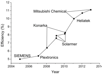
The organic solar cells are typically made from conducting and semiconducting organic materials including polymers and small molecules. The first highly conductive organic polymer, doped polyethylene, was discovered and developed by Hideki Shirakawa, Alan Heeger, and Alan MacDiarmid in 1977 for which they won the Nobel Prize in Chemistry in 2000 [11]. In 1986 C. Tang successfully made the first working heterojunction organic solar cell from copper phthalocyanine (CuPc) and a perylene tetracarboxylic derivative [12]. The device showed an efficiency of about 1% with bi-layer architecture. Then Sariciftci [13] reported the first polymer/buckminsterfullerene (C60) heterojunction device in 1993. In 1994, Yu [14] made the first polymer bulk heterojunction solar cell with poly[2-methoxy-5-(2-ethylhexyloxy)-1,4-phenylenevinylene] (MEH-PPV) and C60. In such a cell an acceptor (C60) and a donor (MEH-PPV) component were mixed and processed simultaneously to act as the active film. After this work, the bulk heterojunction configuration became an important device configuration in this research. Organic solar cells developed very rapidly during the last decade (Figure 1.2). Up to date, a laboratory efficiency record of 11.1% has been achieved by Mitsubishi Chem. (Figure 1.1 & Figure 1.2). However, compared to other technologies, the relatively low efficiency of organic solar cells, together with their short lifetime, limit their large-scale commercialization.
Figure 1.2 Evolution of power conversion efficiency of organic solar cells in the last decade
2004 2006 2008 2010 2012 2014 5 6 7 8 9 10 11 12 Heliatek Mitsubishi Chemical Solarmer Konarka Plextronics E ffi ci ency (% ) Year SIEMENS
7
1.3. Basic knowledge of organic solar cells
To better understand the operational mechanism of organic solar cells, the basic knowledge of organic chemistry and organic solar cells (OSCs) is introduced in this section.
1.3.1.
Organic semiconductors and their applications in solar cells
Conjugated semiconducting polymers are long-chain carbon-based large molecules. Some of them show good electrical and optical properties and have many applications in electronic and optoelectronic devices.
In 1958, Giulio Natta first synthesized the linear polyethylene, but the conductivity of this crystalline polyethylene was very low. Until 1977, the conductivity of polyethylene was improved remarkably by doping halogen elements [15]. It has been reported that the conductivity can be enhanced to be close to 560 Ω-1∙cm-1
when the polyethylene film is doped with halogen or arsenic pentafluoride ions [16]. Later in 1982, Weinberger et al. [17] investigated polyethylene as an active material in organic solar cells. The initial device performance was poor. Then different polythiophenes [18], poly(p-phenylene vinylene) (PPV) [19] and PPV derivatives (e.g., MEH-PPV (Figure 1. 3) [14]) were introduced into organic PV field. The highly regioregular poly(3-hexylthiophene) (P3HT) (Figure 1. 3) came to become the material of choice starting from 1990s. Since then extensive studies have been carried out on P3HT-based solar cells. Recently, low bandgap polymers, such as Poly[2,6-(4,4-bis-(2-ethylhexyl)-4H-cyclopenta
[2,1-b;3,4-b′]dithiophene)-alt-4,7(2,1,3-benzothiadiazole)] (PCPDTBT, Eg = 1.46 eV) and
Poly({4,8-bis[(2-ethylhexyl)oxy]benzo[1,2-b:4,5-b′]dithiophene-2,6-diyl}{3-fluoro-2-[(2-eth ylhexyl)carbonyl]thieno[3,4-b]thiophenediyl}) (PTB7, Eg = ~ 1.8 eV) (Figure 1. 3), are
intensively investigated as active materials in organic solar cells due to their ability to harvest more photons from the solar spectrum.
1.3.2.
The electronic structure of conjugated polymers
Conjugated polymers have long chains consisting of carbon atoms. These carbon atoms form alternating single (σ) and double bonds (π). Following the law of linear combination of atomic orbitals and the hybrid orbital theory, due to this conjugated structure, the electrons in double bonds can delocalize over several backbone carbon atoms and form a delocalized π electron system which gives the polymer semiconducting properties.
8
Figure 1. 4 illustrates the structure, electron cloud distribution and bonding π orbital/anti-bonding π* orbital of ethylene. This is the simplest conjugated molecule. The carbon atom has an electronic configuration of 1s22s22p2. When forming bonds with other atoms, the 1s2 electrons do not participate in bonding since these electrons are strongly bounded to the nucleus. For the 2s2 and 2p2 orbitals, in the case of ethylene, each carbon atom makes covalent σ bonds with two hydrogen atoms, a single and double bond with the other carbon atom. To achieve this goal, the 2s and the in-plane 2px and 2py orbitals overlap with the
adjacent carbon atom to form three degenerate sp2hybridized orbitals (termed sp2orbitals). These hybridized orbitals form three in-plane σ bonds with the other atoms. These hybridized orbitals form three in-plane σ bonds with the other atoms. These single bonds are strong and rigid. The electrons are localized over the two bonded atoms and they are associated with a large bonding energy.
Figure 1. 3 Some conjugated polymers investigated in PV cells. Top: Polyethylene, poly(p-phenylene vinylene) (PPV), poly(2-methoxy-5-(20-ethyl- hexyloxy)-1,4-phenylvinylene) (MEH-PPV), poly(3-hexylthiophene) (P3HT). Bottom:
PCPDTBT, PTB7.
9
The remaining 2pz orbitals of each carbon atom are extended out of the plane of sp2orbitals and
these pz orbitals interact with each other producing a π bond. Electrons forming such double
bonds are delocalized with distribution located above and below the plane of the single bonds. The π bond lowers its bonding energy through splitting bond into two molecular orbitals (the bonding π orbital and the anti-bonding π* orbital, Figure 1. 4). In the ground state, both electrons of the π bond lie in the bonding orbital since this orbital has lowest energy. The highest energy level occupied by electrons is bonding π orbital and referred to as the highest-occupied molecular orbital (HOMO). Similarly, the anti-bonding π* orbital is termed as the lowest unoccupied orbital (LUMO).
In the case of ethylene, each carbon atom donates one electron to the π system. When the conjugation length increases, more and more electrons and orbitals participate in bonding. The π molecular orbitals are delocalized over a longer and longer distance as the molecule gets larger. In the meanwhile, the gap between the HOMO and LUMO gets smaller and smaller. The evolution of π molecular orbitals in conjugated polymers with increasing conjugation length is shown in Figure 1. 5.
Figure 1. 5 Evolution of π molecular orbitals in conjugated polymers with increasing conjugation length
Theoretically, Hückel theory [20] predicts a continuous ladder of electronic states in an infinitely long conjugated polymer. But in practice, this continuous ladder splits into two bands associated with a lattice deformation to lower the total energy of the system, resulting in a gap opening up at the Fermi level. Hence, the highest-occupied molecular orbital of the lower band is the HOMO, the lowest unoccupied orbital is the LUMO and the energy difference between HOMO and LUMO is the bandgap (Figure 1. 5). Typically, the bandgap is in the order of 2 ~ 3
10
eV, e.g., ~ 2.1 eV for P3HT, or even smaller for low bandgap conjugated polymer, e.g., ~ 1.8 eV for PTB7 [21].
In fact, conjugated polymer backbones may consist of atoms of some other elements or fused rings, e.g., sulfur atoms, as shown in Figure 1. 3. This replacement can affect the electronic structures [22] of the polymers and thus their properties. In the meanwhile, the side-chains can alter the crystallinity, solubility and also the electronic structure of the polymers [23,24]. The hetero-atom together with the side-chains allow a great tunability of polymer properties.
1.3.3.
Excitons and polarons in organic semiconductors
An exciton is a quasiparticle formed by an electron and an electron hole which are attracted to each other by electrostatic Coulomb force. It exists extensively in insulators, semiconductors and in some liquids.
An exciton can be formed by photo-induced excitation in semiconductors, which excites an electron to conduction band from valence band. In semiconductors with large dielectric constants and small energy gaps, the electric field screening tends to reduce the coulomb attraction force between electrons and holes. This screened Coulomb interaction together with the small effective mass of electron, the binding energy of excitons is typically small and on the scale of 0.01 eV. Thus the excitons can extend over many molecular units [25]. This type of excitons are termed as Wannier-Mott exciton [26]. Whereas in organic semiconductors, the dielectric constants are relatively lower (~ 3 to 4) as compared to their inorganic counterparts, leading to a larger screening length and thus a larger binding energy. The binding energy of excitons is typically in the order of 0.4 ~ 0.5 eV [27], with a variation range from 0.1 eV to > 1 eV [28,29]. In this case, the term Frenkel exciton is applied [26]. Since the high binding energy, the Frenkel excitons usually reside on one molecule. Moreover, Frenkel excitons in organic semiconductors have a relatively short lifetime in the scale of nanoseconds and a short diffusion length (typically ~ 10 nm) [30,31]. If not dissociated, the excitons can relax to ground state by photon or phonon emission.
There are two kinds of excitons in organic semiconductors: singlet and triplet excitons. Singlet excitons have total spin S = 0. They are generated directly from photon absorption with spin conservation as they are in ground state. The triplet excitons have total spin S = 1 with three possible linear combinations of wavefunctions. They normally cannot be gained from direct photon absorption but can be converted from singlet by intersystem crossing (time scale ~ 10
11
ps) (Figure 1. 10). The triplet excitons have lower energy than singlet due to their larger electron-hole spatial overlap [32].
If the excitons are separated, for instance, by an energetic driving force originated from the difference in the electronic levels of the donor and acceptor materials in organic solar cells [33,34], a positive (hole) and a negative (electron) charge are generated. The presence of a hole or electron charge in organic semiconductors will lead to a local distortion of polymer chains; the coupling of charge and the induced structural relaxation is termed polarons. The presence of polarons creates two new states in the bandgap (since the lattice relaxation lowers the total energy) and thus introduces new absorption transitions (Figure 1. 6).
Figure 1. 6 Polaronic (positive and negative polaron) and excitonic (exciton) energy levels and the associated sub-bandgap transitions. Transitions (E2 & E4) in dash-line are symmetrically disallowed.
1.3.4.
Photo-conversion process
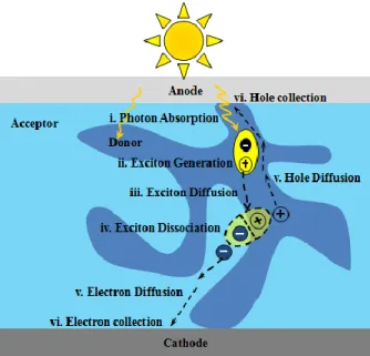
The complete photo-conversion process consists of six steps in organic solar cells. In bulk heterojunction organic solar cells these steps include: (i) absorption of photons, (ii) generation of excitons, (iii) diffusion of excitons, (iv) dissociation of excitons at the donor/acceptor interface, (v) charge transport to electrodes (holes to anode and electrons to cathode) and (vi) charge collection at the electrodes. These six steps are shown in Figure 1. 8. More details about the concept of bulk heterojunction organic solar cells will be given in Section 1.3.5 and 1.4.
1.3.4.1. Absorption of photons and generation of excitons
When sunlight reaches the earth, part of it is scattered by molecules, aerosols and dust particles in the atmosphere; other part of it is absorbed by different gases in the atmosphere, such as oxygen, O3, H2O, CO2. Hence, the intensity and spectrum of sunlight that reaches the Earth’s
surface significantly depend on the length of the light path through the Earth’s atmosphere, whereas this length varies during the day time and also depends on latitude and time of year. In practice, the term Air Mass (AM), ratio of any actual sunlight path length to the minimum
12
value (when the sun is directly overhead, i.e. at the zenith), is usually used to help characterize the spectral content and intensity of solar radiation after traveling through the Earth’s atmosphere. The AM value is given by Equation 1. 1 [35]:
cos 1
AM Equation 1. 1
Where θ is the angle of incident (θ = 0 when the sun is directly overhead) (Figure 1. 7). Hence, just outside the earth’s atmosphere, the solar energy intensity is about 1353 W/m2
[35], and the spectral distribution is referred to as Air Mass zero (AM 0) radiation spectrum. An AM 1.5 (θ = 48.2° [36]) which has an intensity of 1000 W/m2 is usually used as standard spectrum to characterize the photovoltaics. The AM 0 and AM 1.5 spectra are shown in Figure 1. 9.
Figure 1. 7 Illustration of AM 0, AM 1.5 and AM X. Note that at the zenith, the sun is directly overhead and θ = 0; AM 0 is the solar spectrum just above the atmosphere at θ = 0; AM 1.5 is the solar spectrum with an incident angle of 48.2° from the
zenith; X = 1/cosθ.
When sunlight reaches the Earth’s surface and strikes a solar cell, part of it will be scattered, reflected, and absorbed by the encapsulation materials and electrodes. Part of the remaining light, successfully reaching the active layer, will be absorbed by the active layer.
The efficiency of photon absorption depends on the thickness and absorption coefficient of the active materials. The absorption coefficient is determined by the components of the active layer. For poly(3-hexylthiophene) (P3HT) with a bandgap of about 2.1 eV, its absorption can cover the visible spectrum up to 660 nm (Figure 1. 9). Considering the absorption coefficient of a layer composing of a blend of P3HT and [6,6]-phenyl-C61-butyric acid methyl ester (PCBM) to be about 105 cm-1, ∼300 nm thick layers absorb most of the light [37], which is much thinner than silicon solar cells. But due to their modest charge transport properties (e.g., short exciton
13
diffusion length ~ 4 nm to 10 nm [38]), the optimal thickness of active layer for P3HT:PCBM blend is between 100 nm and 200 nm [38–40]. Developing new active materials such as low bandgap polymers (e.g., PTB7) is currently a promising approach to improve light absorption efficiency in organic solar cells.
Figure 1. 8 The six steps of photo-conversion process in bulk heterojunction cells
When a photon is absorbed, it will promote an electron from the ground state S0 into higher
lying unoccupied levels, such as S1 and Sn>1, creating a singlet exciton. The singlet excitons in
higher levels (Sn>1) then relax back to S1 through internal conversion by phonon emission. The
excitons in S1 can also relax to the ground S0 state either by radiative (via photon emission and
this phenomenon is termed fluorescence) or non-radiative (such as via phonon emission) recombination (Figure 1. 10).
Singlet excitons may convert to triplet excitons through intersystem crossing. Triplet excitons are most likely to relax to ground state through phonon emission. Triplet excitons can also decay to ground state radiatively but with a much longer lifetime (μs - ms) than singlet recombination. This triplet radiative process leads to photon emission termed phosphorescence.
14
Figure 1. 9 AM 0 and AM 1.5 solar spectra [41] and absorbance of P3HT
Figure 1. 10 Jablonski diagram of light absorption process in conjugated polymers
1.3.4.2. Diffusion of excitons
As shown in Figure 1. 11, we use Förster and Dexter mechanisms to interpret the exciton diffusion process, respectively [40,42]. According the Förster mechanism, it involves the long-range electrostatic coupling between the excitation transition dipoles located at the initial and final sites. In the case of triplet excitons, they diffuse following a short-range exchange (Dexter-type) mechanism relying on the orbital overlap between adjacent sites. As a result, singlet excitons diffuse more rapidly than triplets. But as mentioned in Section 1.3.3, the lifetime of singlet excitons is on the scale of nanosecond, while triplet excitons have a rather longer lifetime (μs - ms). The actual diffusion efficiency of singlets and triplets to the Donor/Acceptor (D/A) interface depends on the actual device system [40].
0 500 1000 1500 2000 2500 0.0 0.5 1.0 1.5 2.0 2.5 Normal iz ed absorbance of P 3HT ( A .U.) S pectr al irr adi acne (W m -2 nm -1 ) Wavelength (nm) AM 0 AM 1.5 Maximum absorption wavelength of P3HT: ~ 660 nm 0.0 0.4 0.8 1.2 1.6 2.0
15
Förster mechanism for singlet exciton (long-range electrostatic coupling ~ 30-100 Å)
Dexter mechanism for triplet excitons (short-range exchange ~ 6-20 Å)
Figure 1. 11 Förster and Dexter diffusion mechnaisms for singlet and triplet excitons, respectively (Adopted from [42])
1.3.4.3. Dissociation of excitons
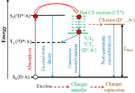
When the excitons reach the donor/acceptor (D/A) interface, if they do not recombine, they may be separated at this interface by an energetic driving force originated from the difference in the electronic levels of the donor and acceptor materials [33,34]. An exciton is a quasi-particle formed by a Coulomb-bound electron-hole pair which is initially located on one molecule. The dissociation of excitons at the D/A interface are generally considered to involve two steps [40,43–45] (Figure 1. 12). First, the exciton dissociates into a charge transfer (CT) state (D+/A-). In this state, the hole sits in the donor molecule and electron travels to the acceptor molecule by hopping. The next step is that the CT exciton separates into charge-separated (CS) states and finally free charge carriers. The final energy of CS state, Efinal
= ID + EA (ID is the ionization potential of donor, EA is the electron affinity of the acceptor and
Efinal is the energy level of completely unbound hole-electron pair (Figure 1. 12)) can be
approximately estimated from the energy difference between the LUMO of the acceptor and HOMO of donor [40]. That is to say, the dissociation occurs when the energy of exciton (energy difference of donor LUMO and donor HOMO) is larger than Efinal [45]. CT excitons
could recombine to the ground state, termed geminate recombination. The recombination of CS carriers is termed non-geminate recombination [46].
The mechanism of CT excitons is still under debate. A new excitation mechanism of CT excitons was proposed recently [44,47]. According to this new mechanism an excited CT exciton (also named hot CT excitons, with excess energy than the CT exciton lying in the lowest CT state) could be directly formed by photon absorption (Figure 1. 13).
16
Figure 1. 12 Schematic Jablonski diagram describing the photo-induced charge-carrier formation mechanism in an organic solar cell: S0 is the singlet ground state of the donor or the acceptor, S1 and T1 the first singlet and triplet excited state,
respectively; the left superior 1 and 3 denotes the singlet and triplet excitons; symbol * denotes the excited state; + and – represent the positive and negative charge, respectively.( Adopted from reference [40])
Figure 1. 13 Charge generation process in organic solar cells. Left: indirect formation of CT exciton; right: direct formation of CT exciton by photon absorption (Adopted from reference [44])
1.3.4.4. Transport of charge carriers
Once excitons are separated into free charge carriers, electrons will transport to cathode and holes to anode. Otherwise, non-geminate recombination will occur. Various recombination processes are involved during charge transport: (1) radiative recombination by photon emission; (2) non-radiative recombination by phonon emission; (3) recombination at the sub-bandgap trap states induced by the impurities or defects in the material (Shockley-Read-Hall recombination) [42].
If charges do not recombine, they will travel in the form of polarons (Section 1.3.3) in conjugated organic materials. Polarons moves intra- or inter-molecular by hopping. Compared to the high mobility (on the scale of 102 - 103 cm2 V-1 s-1) in inorganic semiconductors, the
17
mobilities in organic semiconductors are quite low (typically, 10-6-10-3 cm2 V-1 s-1) [40,48]. This modest mobility is owing to the weak electronic couplings, large electron-vibration couplings and disorder packing in polymers. As a result, the polymer morphology and crystallinity affect the transport mobilities significantly [40,48]. If the polymer is well crystallized, the mobility can reach over 1 cm2 V-1 s-1 [40,48].
1.3.4.5. Extraction of charges
Once arriving at the electrodes, polarons may be extracted into the external circuit. Metal conductors form two kinds of contacts with semiconductors: ohmic or Schottky contact, determined by the work function of the metal ΦM, work function (ΦSC)and electronic affinity
(χSC) of the semiconductors [49]. Here, the work function ΦM is the minimum energy needed to
remove an electron to vacuum from the Fermi level of the metal; ΦSC isthe minimum energy
needed to remove an electron to vacuum from the Fermi level of the semiconductor; the electronic affinity χSC is the energy required to promote an electron to the vacuum energy level
from the bottom of the conduction band. The formation conditions of these two contacts are shown in Figure 1. 14.
Figure 1. 14 Schematic of metal-semiconductor contacts. Note that the black dots at the metal-semiconductor interface represent electrons and circles represent holes; Ev is the energy level of the top of the valance band and Ec is the energy level
of the bottom of the conduction band; Evacuum is the energy level of vacuum while EF is the Fermi level.
In ohmic contact, there is no potential barrier for charges to travel across the contact; while for Schottky contact, there is a potential barrier Eb (given by Equation 1. 2) at the interface (Figure
18
SC M
b Φ χ
E Equation 1. 2
If highly doped, the semiconductors will have a narrow space-charge region width and a narrow Schottky barrier Eb. When the barrier is sufficiently narrow, the electrons can tunnel
from the metal to the semiconductor and from the semiconductor to the metal [50]. In this case, the Schottky contact becomes ohmic due to tunneling.
In the organic semiconductors, the metal-semiconductor contact is complex due to factors such as interfacial charge-density redistributions, geometry modifications, and/or chemical reactions occur at the interface. These factors significantly affect the charge collection efficiency [40,51].
1.3.5.
Architectures of organic solar cells
1.3.5.1. General architecture of organic solar cells
In general, the organic solar cells are composed of several thin layers (Figure 1. 15).
− The substrate can be typically a thin glass or a flexible and transparent substrate such as Polyethylene terephthalate (PET).
− The anode should be transparent since it locates before the active layer. Typically it is indium tin oxide (ITO) or fluorine doped tin oxide (FTO). ITO has bandgap of 3.7 eV, thus most photons can travel through it. For visible light the transmittance of commercial ITO is higher than 80% [52]. The back electrode does not need to be transparent and is typically a layer of aluminum or silver or gold.
− Generally speaking, a hole extraction layer (HEL) is inserted between the anode and the active layer. This layer is also thin and highly transparent. It typically has a work function very close to the ionization potential of the donor component in the active layer to facilitate hole extraction. The most common material for HEL is Poly(3,4-ethylenedioxythiophene):Polystyrene sulfonate (PEDOT:PSS). Similarly, there is an electron extraction layer (EEL) inserted between the active layer and cathode. Calcium and lithium fluoride are frequently used for this layer.
− The active layer is deposited onto the HEL layer. It is the layer responsible to absorb photons and it is the main part of the solar cell. It normally consists of a donor material and an acceptor material.
19
Depending on the variations within the active layer, there are four common architectures which will be described below.
1.3.5.2. Single layer cells
The active layer consists of just one semiconductor material. This layer forms a Schottky contact with an electrode. Due to the energy band bending of the Schottky contact excitons generated in the active layer will be spitted into electrons and holes and transported to the corresponding contact electrode. The drawback in such device structure lies in the serious charge recombination during transport.
1.3.5.3. Planar heterojunction cells
This structure is typically composed of two layers: one from the donor material and the other from the acceptor material. The excitons are transported to the donor/acceptor interface and then dissociated there. Solar cells with this device structure is limited by the small D/A interface since only a limited portion of excitons can reach the D/A interface and dissociate there.
1.3.5.4. Bulk heterojunction cells
In this structure, the donor and acceptor materials are well mixed in solution first. They are then deposited onto a substrate resulting in the formation of a number of small domains allowing a large interfacial area (Figure 1. 8). Due to the enlarged interfacial area, more excitons can reach the donor/acceptor (D/A) interface in organic solar cells. The morphology of active layer therefore affects the charge separation significantly. We used this architecture in this thesis and more details will give in the following Section 1.4.
1.3.5.5. Tandem solar cells
Because most organic materials have a limited absorption window, tandem architecture is introduced to combine solar cells based on different active materials to boost photon harvest efficiency. In such device structure two or more organic solar cells are deposited on each other to form a system in series. The component cells have different absorption window and the combination of them can thus achieve higher photon absorption efficiency. The short circuit current in a tandem cell is limited by the cell which has the lower/lowest short circuit current.
20
Figure 1. 15 General architecture of organic solar cell: HEL denotes the hole extraction layer, and EEL the electron extraction layer.
In addition, some new architectures for organic solar cells are currently being developed based on the above-mentioned four device structures. Examples of these structures include optical fiber based architecture and folded reflective architecture [30].
1.4. Organic bulk heterojunction solar cells using polymers and small
molecules
The organic bulk heterojunction solar cells (OSCs) using PEDOT:PSS as anodic buffer layer are used in this thesis. Thus the PEDOT:PSS and the photoactive layer for OSCs are introduced in this section.
1.4.1.
Hole extraction layer: PEDOT:PSS
The poly(3,4-ethylenedioxythiophene) (PEDOT) is an intrinsically conducting polymer built from 3,4-ethylenedioxythiophene (EDOT) monomers. PEDOT is insoluble in many common solvents and unstable in air in its neutral state. These disadvantages limit its industrial applications. Fortunately, these problems can be solved by incorporating oxidant sodium peroxodisulfate (Na2S2O8) and modifiable proportion of poly(styrene sulfonic acid) (PSS) into
the solution and resulting in an aqueous dispersion of PEDOT:PSS. In such solution PEDOT is in an oxidized state (Figure 1. 16) and it shows high stability when oxidized [53,54]. PSS is water soluble and acts as a template polymer in the dispersion and thus forms a PEDOT-PSS complex. It has two functions in the complex: (1) PSS acts as a charge balancing dopant which supplies counter ions and thus, accompanied with sodium peroxodisulfate (Na2S2O8), keeps the
PEDOT in an oxidized state [55]; (2) PSS can make the PEDOT segments (oligomers with about 6 to 18 repeating units) forming PEDOT-PSS complex and thus keep them dispersed in
21
the aqueous solution (Figure 1. 17) [55–58]. The PEDOT to PSS ratio can affect the film conductivity significantly, and to some extent, the conductivity decreases with increasing PSS content [56].
PEDOT:PSS is commonly used as the buffer layer of anodic electrode in OSCs [59–61]. Generally speaking, the work function of PEDOT:PSS (4.7-5.4 eV [62]) is normally higher than ITO (4-5 eV [63]) and thus leading to efficient hole extraction. In addition, the spin-coated PEDOT:PSS film can smoothen the rough ITO surface and reduces the chance of short-circuits [64,65]. The PEDOT:PSS layer located between the ITO and photoactive layer may also help to prevent oxygen diffusing into the photoactive layer. The migration of oxygen will oxidize the polymer like P3HT which is believed to be one of the device performance degradation mechanisms of OSCs [66,67].
Figure 1. 16 Structures of PEDOT and PSS, adopted from reference [53]
Figure 1. 17 Schematic of PEDOT:PSS complex, adopted from reference [55]
In PEDOT:PSS films, the PEDOT grains are surrounded by the excess PSS after spin-coating. Upon drying, a solid film will be obtained and the film is comprised of horizontal layers of flattened PEDOT-rich grains embedded in quasi-continuous PSS lamellas, forming a granular structure [56–58,68]. The average diameter of such grains is in the range of 20–80 nm [57,58]. The thickness of the PSS shells has been found to be about 35±5 Å [69–71]. Since PEDOT is a conducting component while PSS has only a weak conductivity, the PEDOT-rich core has a higher conductivity than the PEDOT-depleted PSS shell. Therefore, charges can transport more efficiently along the backbone in the grains than between them due to the charge transport barrier induced by the insulating PSS shell [56]. Hence in such a granular structure, the
22
electrical conductivity is controlled by the hole transport in the PEDOT oligomers, the hopping between PEDOT oligomers and between the PEDOT-rich gains with a PSS barrier [56,58]. Consequently, the conductivity of PEDOT:PSS film is rather low. For instance, pristine Clevios™ P – Heraeus PEDOT:PSS used in this work has the maximum conductivity of ~ 1 S/cm [72].
Many techniques have been applied to enhance the conductivity of PEDOT:PSS, such as applying post-deposition thermal annealing [73,74], adding high boiling solvents (e.g., glycerol or sorbitol [75–77]), modifying synthetic conditions [78,79], improving the wetting of ITO surface (e.g., silanes [80]), adding polar solvent (e.g., dimethylsulfoxide [81]), and varying the PEDOT to PSS ratio [80,82]. In this thesis we mainly apply the thermal annealing and high boiling additives to improve the conductivity of PEDOT:PSS films.
In addition, the thickness of PEDOT:PSS used in OSCs is typically in the scale of several tens of nanometers [45,83–85]. A PEDOT:PSS layer thicker than such thickness will reduce the transmission significantly [72] despite a decreased sheet resistance decreases [86].
1.4.2.
Bulk heterojunction
As mentioned in Section 1.3.1, various organic polymers and small molecules have been investigated for their application in organic solar cells. In particular, the conjugated polymer poly(3-hexylthiophene-2,5-diyl) (P3HT) and the small molecule derivatives of fullerene, [6,6]-Phenyl C61 butyric acid methyl ester (PCBM), form one of the most popular organic solar cell active layer components. Here, P3HT is used as a donor material while the PCBM are as the acceptor materials. During the device fabrication process, P3HT and PCBM are dissolved in an organic solvent, such as chlorobenzene and di-chlorobenzene. They blend of them is deposited as the active layer with a controlled morphology, in order to reach the highest device performance.
1.4.2.1. Donor material: P3HT
The polythiophene is a conjugated polymer made of thiophene monomers. P3HT is one derivative of polythiophene and it has hexyl groups attached at the position No. 3 of polythiophene (Figure 1. 18).
23
Figure 1. 18 Chemical structures of poly(3-hexylthiophene-2,5-diyl)
1.4.2.1.1. Regioregularity
When polymerizing 3-hexylthiophene monomers to synthesize P3HT, there are three possible asymmetric couplings, they are (Figure 1. 19):
1) 2, 5', or head-tail (HT) coupling. 2) 2, 2', or head-head (HH) coupling. 3) 5, 5', or tail-tail (TT) coupling.
As a result, the term regioregularity is used to describing repetition degree of couplings in a polymer. For example, 98% head-tail regioregular P3HT means that the ratio between the number of HT coupling and the sum of all these three types of couplings is 98%.
It is reported that regiorandom P3HT has low charge mobility due to the random sequence of HT, HH and TT building blocks and the resultant poor intermolecular orbital overlap [87–89]. Highly regioregular P3HT has a highly planar conformation [90] which favors a close intermolecular π-stacking in lamella fashion (Figure 1. 20) [89,91–94] and improves the charge mobility. It has been reported that, with a lamella packing, the mobility of P3HT can reach as high as 0.1 cm2 V-1 s-1 [91,95,96].
![Figure 1.1 Evolution of solar cells’ power conversion efficiency record for all types of photovoltaics [10]](https://thumb-eu.123doks.com/thumbv2/123doknet/14636225.734876/26.892.136.761.378.753/figure-evolution-solar-cells-conversion-efficiency-record-photovoltaics.webp)

![Figure 1. 9 AM 0 and AM 1.5 solar spectra [41] and absorbance of P3HT](https://thumb-eu.123doks.com/thumbv2/123doknet/14636225.734876/35.892.248.648.133.416/figure-solar-spectra-absorbance-p-ht.webp)
![Figure 1. 25 Effects of R s and R sh on fill factor, J sc and V oc [116].](https://thumb-eu.123doks.com/thumbv2/123doknet/14636225.734876/53.892.172.726.106.317/figure-effects-r-r-sh-factor-j-sc.webp)
![Figure 1. 32 Extinction spectra of a 2D array of the Au nanoparticle pairs with the interparticle center-to-center spacing as the parameter [182]](https://thumb-eu.123doks.com/thumbv2/123doknet/14636225.734876/63.892.112.735.103.316/figure-extinction-spectra-nanoparticle-interparticle-center-spacing-parameter.webp)