HAL Id: tel-01952831
https://tel.archives-ouvertes.fr/tel-01952831
Submitted on 12 Dec 2018HAL is a multi-disciplinary open access archive for the deposit and dissemination of sci-entific research documents, whether they are pub-lished or not. The documents may come from teaching and research institutions in France or abroad, or from public or private research centers.
L’archive ouverte pluridisciplinaire HAL, est destinée au dépôt et à la diffusion de documents scientifiques de niveau recherche, publiés ou non, émanant des établissements d’enseignement et de recherche français ou étrangers, des laboratoires publics ou privés.
Single-event effects from space and atmospheric
radiation in memory components
Alexandre Louis Bosser
To cite this version:
Alexandre Louis Bosser. Single-event effects from space and atmospheric radiation in memory com-ponents. Micro and nanotechnologies/Microelectronics. Université Montpellier; Jyväskylän yliopisto, 2017. English. �NNT : 2017MONTS085�. �tel-01952831�
DEPARTMENT OF PHYSICS, UNIVERSITY OF JYVÄSKYLÄ LIRMM, UNIVERSITY OF MONTPELLIER/CNRS
RESEARCH REPORT No. 10/2017
SINGLE-EVENT EFFECTS OF SPACE AND ATMOSPHERIC RADIATION
ON MEMORY COMPONENTS
by
Alexandre Louis BOSSER
Academic Dissertation for the Degree of Doctor of Philosophy
To be presented, by permission of the Faculty of Mathematics and Science of the University of Jyväskylä and the President of the University of Montpellier, for public examination in Auditorium FYS 1 of the
University of Jyväskylä on December 20th, 2017 at 12 noon.
Jyväskylä, Finland 2017
3 Alexandre Louis Bosser, 1991-
Single-event effects of space and atmospheric radiation on memory components Jyväskylä: University of Jyväskylä, 2017, 103 pages
Research report No. 10/2017, Department of Physics, University of Jyväskylä ISSN 0075-465X; 10/2017
ISBN paper copy: 978-951-39-7311-7 ISBN electronic: 978-951-39-7312-4
5
Preface
I would like to express my deepest gratitude to my supervisors, Prof. Ari Virtanen, Dr Luigi Dilillo and Dr Arto Javanainen, who showed great dedication at their task and were always available for fruitful discussions, useful advice and support; I know that adequate supervision and good morale are key to the success of doctoral studies. I was also fortunate to be given every possible opportunity to present my research in international conferences, which greatly improved my visibility and my expertise. I am very thankful for the exceptional work environment you have provided for me.
I would also like to thank my colleagues at RADEF and LIRMM, for the friendly work atmosphere and the support they offered. In particular, I want to acknowledge the major contribution of Dr Viyas Gupta, who started his PhD at LIRMM at the same time as I did; Viyas and I worked together on the topics presented in this manuscript, preparing and carrying out the test campaigns, processing and discussing the data, and writing the publications. It was a real pleasure working with you, and I hope we will collaborate again in the future!
I’m also grateful to my reviewers, Prof. Simone Gerardin and Prof. Ronald Schrimpf, and to my Opponent Prof. Fernanda Lima Kastensmidt, for the work they have accomplished and the useful comments they provided on my thesis on short notice. I would like to give special thanks to Prof. Lima Kastensmidt for travelling all the way to Finland for my defense.
This research was supported in part by the European Space Agency (ESA/ESTEC Contracts 4000111630/14/NL/PA and 4000111085/14/NL/PA), the European Commission (EU-HORIZON-2020/RIA/R2RAM, project ID 640073, 2015-2016) and the Academy of Finland under the Finnish Centre of Excellence Programme 2012-2017 (Project 2513553, Nuclear- and Accelerator-Based Physics).
Finally, I would like to thank my family, my friends, and most importantly my fiancée Anni Herranen, who were always there to support me and cheer me up when I needed it. Thank you for carrying me through five long, cold, dark Finnish winters!
6
Abstract
Electronic memories are ubiquitous components in electronic systems: they are used to store data, and can be found in all manner of industrial, automotive, aerospace, telecommunication and entertainment systems. Memory technology has seen a constant evolution since the first practical dynamic Random-Access Memories (dynamic RAMs) were created in the late 60's. The demand for ever-increasing performance and capacity and decrease in power consumption was met thanks to a steady miniaturization of the component features: modern memory devices include elements barely a few tens of atomic layers thick and a few hundred of atomic layers wide.
The side effect of this constant miniaturization was an increase in the sensitivity of these devices to radiation. Since the first radiation-induced single-event effects (SEEs) were identified in satellites in the late 70’s [1] and particle-induced memory upsets were replicated in laboratory tests [2], radiation hardness has been a concern for computer memory manufacturers and for systems designers as well. In the early days, the need for data storage in radiation-rich environments, e.g. nuclear facilities, particle accelerators and space, primarily for military use, created a market for radiation-hardened memory components, capable of withstanding the effects of radiation ; however, this market dwindled with the end of the Cold War and the loss of government interest [3]. In a matter of years, the shortage of available radiation-hard components led system designers to turn to so-called Commercial Off-The-Shelf (COTS) components, with the added benefit of higher performance at a lower cost.
Since COTS devices are not designed with radiation hardness in mind, each COTS component must be assessed before it can be included in a system where reliability is important – a process known as Radiation Hardness Assurance (RHA) [4]. This has led to the emergence of radiation testing as a standard practice in the industry (and in the space industry in particular). Irradiation tests with particle accelerators and radioactive sources are performed to estimate a component’s radiation-induced failure rate in a given radiation environment, and thus its suitability for a given mission.
The present work focuses on SEE testing of memory components. It presents the requirements, difficulties and shortcomings of radiation testing, and proposes methods for radiation test data processing; the detection and study of failure modes is used to gain insight on the tested components. This study is based on data obtained over four years on several irradiation campaigns, where memory devices of different technologies (static RAMs, ferroelectric RAM, magnetoresistive RAM, and flash) were irradiated with proton, heavy-ion, neutron and muon beams. The yielded data also supported the development of MTCube, a CubeSat picosatellite developed jointly by the Centre Spatial Universitaire (CSU) and LIRMM in Montpellier, whose mission is to carry out in-flight testing on the same memory devices. The underlying concepts regarding radiation, radiation environments, radiation-matter interactions, memory component architecture and radiation testing are introduced in the first chapters.
Keywords: Radiation effects, memory, COTS, RAM, SRAM, FRAM, MRAM, flash, single-event effect, radiation testing
7
Résumé
Les composants mémoires sont omniprésents en électronique : ils sont utilisés pour stocker des données, et sont présents dans tous les champs d’application - industriel, automobile, aérospatial, grand public et télécommunications, entre autres. Les technologies mémoires ont connu une évolution continue depuis la création de la première mémoire vive statique (Static Random-Access Memory, SRAM) à la fin des années 60. Les besoins toujours plus importants en termes de performance, de capacité et d’économie d’énergie poussent à une miniaturisation constante de ces composants : les mémoires modernes contiennent des circuits dont certaines dimensions sont de l’ordre du nanomètre.
L’un des inconvénients de cette miniaturisation fut un accroissement de la sensibilité de ces composants aux radiations. Depuis la détection des premiers effets singuliers (Single-Event Effects, SEE) sur un satellite à la fin des années 70 [1], et la reproduction du phénomène en laboratoire [2], les fabricants de composants mémoires et les ingénieurs en électronique se sont intéressés au durcissement aux radiations. Au début, les besoins en stockage pour applications civiles et militaires – comme le développement d’accélérateurs de particules, de réacteurs nucléaires et d’engins spatiaux – créèrent un marché pour les composants durcis aux radiations ; cependant, ce marché s’est considérablement réduit avec la fin de la Guerre Froide et la perte d’intérêt des gouvernements [3]. En quelques années, les ingénieurs durent se tourner vers des composants commerciaux (Commercial Off-The-Shelf Components, COTS), ce qui permit au passage des gains en performance et une réduction des coûts.
Les composants COTS n’étant pas conçus pour résister aux radiations, chaque composant doit être évalué avant d’être utilisé dans des systèmes dont la fiabilité est critique. Ce processus d’évaluation est appelé Radiation Hardness Assurance (RHA) [4]. Les tests aux radiations des composants commerciaux sont devenus une pratique standardisée (en particulier dans l’industrie aérospatiale). Ces composants sont irradiés à l’aide d’accélérateurs de particules et de sources radioactives, afin d’évaluer leur sensibilité, de prédire leur taux d’erreur dans un environnement radiatif donné, et ainsi de déterminer leur adéquation pour une mission donnée.
Cette étude porte sur le test de composants mémoires aux effets singuliers. Les objectifs, difficultés et limitations des tests aux radiations sont présentés, et des méthodes d’analyse de données sont proposées ; l’identification et l’étude des modes de défaillance sont utilisées pour approfondir les connaissances sur les composants testés. Cette étude est basée sur de nombreuses campagnes de test aux radiations, effectuées sur une période de quatre ans, pendant lesquelles des mémoires de différentes technologies – mémoires vives statiques (SRAM), ferroélectriques (FRAM), magnétorésistives (MRAM) et mémoires flash – furent irradiées avec des faisceaux de muons, neutrons, protons et ions lourds. Les données générées ont également servi au développement d’un CubeSat développé conjointement par le LIRMM et le Centre Spatial Universitaire de Montpellier, MTCube, dont la mission est l’irradiation de ces mêmes composants en milieu spatial. Les concepts sous-jacents liés aux radiations, aux environnements radiatifs, à l’architecture des composants mémoires et aux tests aux radiations sont introduits dans les premiers chapitres.
Mots-clés: Radiation effects, memory, COTS, RAM, SRAM, FRAM, MRAM, flash, single-event effect, radiation testing
8
Author Alexandre Louis Bosser
Department of Physics, University of Jyväskylä Jyväskylä, Finland
LIRMM, University of Montpellier/CNRS Montpellier, France
email: [email protected]
Supervisors Professor Ari Virtanen
Department of Physics, University of Jyväskylä Jyväskylä, Finland
Dr Arto Javanainen
Department of Physics, University of Jyväskylä Jyväskylä, Finland
School of Engineering, Vanderbilt University Nashville, TN, USA
Dr Luigi Dilillo
LIRMM, University of Montpellier/CNRS Montpellier, France
Reviewers Professor Ronald Schrimpf
Institute for Space and Defense Electronics, Vanderbilt University Nashville, TN, USA
Associate Professor Simone Gerardin
Department of Information Engineering, University of Padova Padova, Italy
Opponent Professor Fernanda Lima Kastensmidt
Institute of Informatics, Federal University of Rio Grande do Sul Porto Alegre, Brazil
9
List of peer-reviewed publications
This doctoral thesis is based in part on the following peer-reviewed publications:
I. A. L. Bosser, V. Gupta, A. Javanainen, G. Tsiligiannis, S. D. LaLumondiere, D. Brewe, V. Ferlet-Cavrois, H. Puchner, H. Kettunen, T. Gil, F. Wrobel, F. Saigné, A. Virtanen and L. Dilillo, “Single-Event Effects in the Peripheral Circuitry of a Commercial Ferroelectric Random-Access Memory” (presented at RADECS 2017, submitted for publication in IEEE Transactions on Nuclear Science)
Contribution: the author had a major role in the experiment’s software and hardware development, took part in the test campaigns, and did most of the data processing and writing. II. A. Bosser, V. Gupta, G. Tsiligiannis, A. Javanainen, H. Kettunen, H. Puchner, F. Saigné, A. Virtanen, F.
Wrobel and L. Dilillo, “Investigation on MCU Clustering Methodologies for Cross-Section Estimation of RAMs”, in IEEE Transactions on Nuclear Science, Vol. 62, no. 6, pp.2620-2626, 2015.
Contribution: the author had a major role in the experiment’s software and hardware development, took part in the test campaigns, and did most of the data processing and writing. III. A. L. Bosser, V. Gupta, G. Tsiligiannis, C. Frost, A. Zadeh, J. Jaatinen, A. Javanainen, H. Puchner, F.
Saigné, A. Virtanen, F. Wrobel, and L. Dilillo, “Methodologies for the Statistical Analysis of Memory Response to Radiation”, in IEEE Transactions on Nuclear Science, Vol. 63, no. 4, pp.2122-2128, 2016. Contribution: the author had a major role in the experiment’s software and hardware development, took part in the test campaigns, and did most of the data processing and writing. IV. L. Dilillo, G. Tsiligiannis, V. Gupta, A. Bosser, F. Saigné and F. Wrobel, “Soft errors in commercial
off-the-shelf static random-access memories”, in Semiconductor Science and Technology, vol. 32, no.1, 2016
Contribution: the author had a major role in the experiment’s software and hardware development, and took part in the test campaigns, data processing and writing.
V. V. Gupta, A. Bosser, G. Tsiligiannis, M. Rousselet, A. Zadeh, A. Javanainen, A. Virtanen, H. Puchner, F. Saigné, F. Wrobel and L. Dilillo, "SEE on Different Layers of Stacked-SRAMs", in IEEE Transactions on Nuclear Science, vol. 62, no. 6, pp. 2673-2678, 2015.
Contribution: the author had a major role in the experiment’s software and hardware development, and took part in the test campaigns and writing.
VI. V. Gupta, A. Bosser, G. Tsiligiannis, A. Zadeh, A. Javanainen, A. Virtanen, H. Puchner, F. Saigné, F. Wrobel and L. Dilillo, "Heavy-Ion Radiation Impact on a 4 Mb FRAM Under Different Test Modes and Conditions," in IEEE Transactions on Nuclear Science, vol. 63, no. 4, pp. 2010-2015, Aug. 2016.
Contribution: the author had a major role in the experiment’s software and hardware development, and took part in the test campaigns.
VII. G. Tsiligiannis, L. Dilillo, V. Gupta, A. Bosio, P. Girard, A. Virazel, H. Puchner, A. Bosser, A. Javanainen, A. Virtanen, C. Frost, F. Wrobel, L. Dusseau, and F. Saigné, "Dynamic Test Methods for COTS SRAMs," in IEEE Transactions on Nuclear Science, vol. 61, no. 6, pp. 3095-3102, 2014.
11
Table of Contents
Preface ... 5
Abstract ... 6
List of peer-reviewed publications... 9
Chapter I – Radiation Environments ... 12
A. Space radiation ... 12
B. Atmospheric radiation ... 15
C. Artificial radiation sources ... 17
Chapter II – Radiation-matter interactions ... 19
A. Photon-matter interactions ... 19
B. Particle-matter interactions ... 20
C. Consequences of irradiation ... 22
D. Useful concepts for radiation testing ... 24
Chapter III – Memory devices ... 27
A. General principles ... 27
B. Memory cell technologies ... 30
C. Device manufacturing ... 32
Chapter IV – Radiation effects on memory components ... 35
A. Total Ionizing Dose (TID) effects ... 35
B. Single-Event Effects (SEEs) ... 37
Chapter V – Radiation testing of memory components ... 45
A. Radiation Hardness Assurance ... 45
B. Testing standards and methodologies ... 46
C. Concepts and metrics for radiation testing ... 47
D. Algorithms for memory testing ... 48
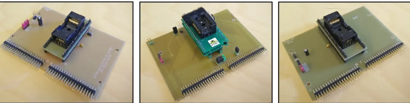
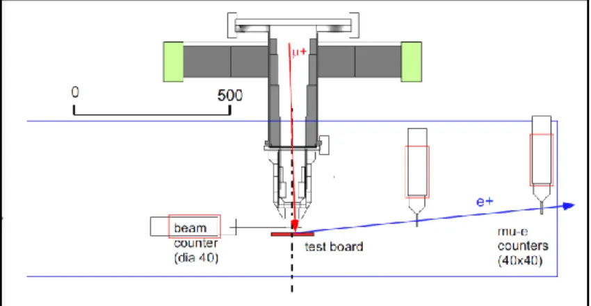
Chapter VI – Experimental setup ... 51
A. Test setups ... 51
B. Data processing ... 56
Chapter VII – Test results and discoveries ... 59
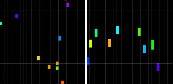
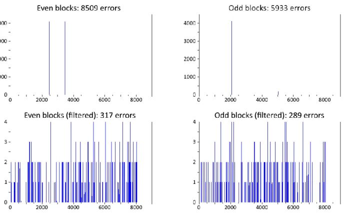
A. Clustering of bit errors in a 90 nm SRAM ... 59
B. Statistical analysis of the radiation response of a 65 nm SRAM ... 62
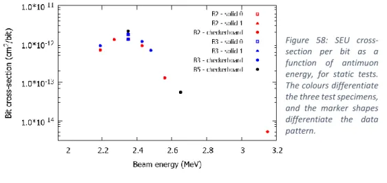
C. Muon-induced Single-Event Upsets in a 65 nm SRAM ... 69
D. Failure mode analysis of an FRAM... 74
E. Effects of heavy-ion radiation on a Single-Level Cell NAND flash memory ... 85
F. Single-Event Latch-ups in an MRAM ... 90
Chapter VIII – Summary ... 94
References ... 95
12
Chapter I – Radiation Environments
Radiation is a term used to designate the emission or transmission of energy, in the form of waves or particles. Although it can sometimes be used to designate acoustic radiation (the propagation of sound waves) or even gravitational radiation (the propagation of gravitational waves), its most commonly accepted meaning (and the one which will be retained in the present thesis) restricts it to electromagnetic radiation and particle radiation.
Electromagnetic radiation is the propagation of electromagnetic waves: this includes radio waves and microwaves, infrared, visible and UV light, X-rays and γ-rays. Particle radiation designates the propagation of energetic (ie. high-speed) particles, which includes (among other particles) electrons, neutrons, protons and heavier ions. These particles may or may not carry electric charge.
A distinction can be made between non-ionizing radiation and ionizing radiation, which has the power to ionize matter (remove electrons from target atoms). However, the boundary between the two is not sharply defined, because different target materials ionize at different energies.
The type, energy and flux of radiation which can be encountered at a given place is referred to as a radiation environment. In the following sections, various typical radiation environments will be described.
A. Space radiation
1) Interplanetary radiation environment
The main source of interplanetary radiation is the Sun, with the higher-energy tail of the spectrum coming from distant stars and supernovae.
The Sun emits electromagnetic radiation across most of the electromagnetic spectrum; while it does emit gamma rays, X-rays, microwaves and radio waves, most of its power output is emitted at wavelengths between 100 nm and 1 mm (which includes ultraviolet, visible and infrared light).
The Sun also emits (among other particles) a continuous stream of electrons, protons, and a few heavier particle species; this stream is known as the solar wind, and can be divided into two main components. The “slow” solar wind is composed almost entirely of electrons and protons, with particle speeds of about 400 km.s-1, while the “high speed” solar wind, which originates from the coronal holes (which are concentrated around the poles, but can be found throughout the Sun’s surface) has particle speeds of 500 to 800 km.s-1 and is slightly richer in heavier elements. Since the Sun’s equator rotates every 27 days, the faster streams emanating from coronal holes form a spiral of expanding high-density plasma traveling outwards into the Solar system (see Figure 1) [5].
13
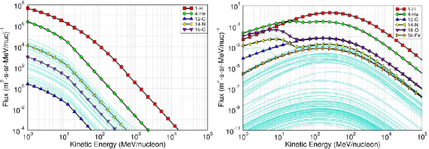
In addition to the continuous solar wind, the Sun occasionally emits massive bursts of plasma, in events known as solar flares and Coronal Mass Ejections (CME). These events originate in regions where the Sun’s magnetic field lines bundle up in to helical structures known as flux ropes [6]. The ejected plasma is mostly made up of protons and electrons, with a small fraction of helium ions (alpha particles) and trace amounts of heavier nuclei, and travels at speeds around 100 km.s-1 to around 3000 km.s-1 [7]. As it travels through interplanetary space, it interacts with the slower solar wind plasma, creating high-density particle “shockwaves”. Altogether, these high-energy particles coming from the Sun are called Solar Energetic Particles (SEP). Figure 2 illustrates the SEP spectrum obtained during the “worst week” starting on 19th October 1989 (a week of unusually high solar activity) [8].
Another source of radiation in interplanetary space are the Galactic Cosmic Rays (GCRs), which are high-energy nuclei, ranging from hydrogen (most common, 89% of the flux) to uranium (traces only). While their origin is being debated, they are known to come from outside of the Solar System, with distant supernovae thought to be a major contributor to the GCR flux. These nuclei have been stripped of all their electrons because of their high energy, hence they carry a high electric charge and can be deflected by magnetic fields [9]. Several models have been developed, which allow the computation of the GCR spectrum and flux near the Earth, outside of the Earth’s magnetosphere [10]–[12]. Figure 3 illustrates the GCR energetic spectrum for some of the most common ion species.
The Sun goes through phases of high and low activity, with a period of around 11 years, called solar cycles. The activity of the Sun influences its radiated power, as well as the number of active regions and coronal holes on its surface, which in turn affect the frequency and magnitude of solar flares and CMEs, and ultimately the SEP spectrum and flux. The GCR spectrum is also affected: during high solar activity, the larger quantity of solar plasma diffusing through the Solar System increases the magnitude of the Heliospheric Magnetic Field (HMF). This means that lower-rigidity (lower-energy) GCR particles (which are coming from outside the Solar System) undergo more deflection by interacting with the HMF when the Sun is at its peak activity: the periods of high solar activity lead to periods of low GCR fluxes, and periods of low solar activity allow for higher GCR fluxes [13].
Figure 2: Maximal differential SEP flux vs kinetic energy per nucleon as a function of atomic number (in near-Earth interplanetary space). The curves for some of the most common ion species are identified. Source: CREME-MC [8], using the CREME 96 SEP model.
Figure 3: Maximal differential GCR flux vs. kinetic energy per nucleon as a function of atomic number (in near-Earth interplanetary space). The curves for some of the most common ion species are identified. Source: CREME-MC [8], using the CREME 96 GCR model.
14
2) Near-Earth radiation environment
The Earth generates a dipole-like magnetic field, with its centre slightly offset from the Earth’s centre, and tilted about 11° with respect to its rotational axis. The origin of this magnetic field is thought to be the motion of electrically conductive liquid iron alloys in the Earth’s outer core, driven by thermal convection and Coriolis forces caused by the rotation of the Earth – an origin theory known as the “dynamo theory” [14]. As they encounter the Earth’s magnetic field, charged particles (such as solar wind plasma, SEPs and GCRs) are deflected by a force known as the Lorentz force, which is proportional to their speed and to the magnitude of the magnetic field. This phenomenon has a two-fold impact on the near-Earth radiation environment.
The particles of low magnetic rigidity1 (i.e. GCRs and high-energy SEP) can be deflected away from the Earth: this geomagnetic shielding effect prevents them from reaching areas where the geomagnetic field is stronger (at low altitudes and high latitudes). Figure 4 illustrates the effect of the geomagnetic shielding on the particle spectrum as a function of magnetic latitude and ion species (which, for fully-stripped GCRs, determines their rigidity).
The trajectories of the lowest-energy, least rigid particles (protons and electrons) are bent so much that they can be trapped in a broad region, extending from a few hundred kilometres to about 60.000 km of altitude, called the Van Allen radiation belts (Figure 5). The belts have a roughly toroidal shape, centered around the Earth’s magnetic centre and aligned with its magnetic equator. Inside the belts, individual trapped particles drift around the Earth, depending on their electrical charge (eastward for electrons, and westward for protons);
additionally, they move along a helicoidal path around the Earth’s magnetic field lines, “bouncing” back and forth between the two magnetic poles [15]-p.22. As the magnetic field lines get closer to the Earth near the poles, these trapped particles may interact with atoms in the upper atmosphere, resulting in the generation of low-energy, “cold” plasma. This phenomenon is also the source of auroral displays.
The particles trapped in the Earth’s magnetic field tend to concentrate at different altitudes depending on their mass and velocity. Traditionally, the Van Allen belts are considered to consist of a smaller inner belt, and a larger outer belt. The inner belt is made of protons (at energies up to 400 MeV) and electrons (at energies up to 5 MeV), while the outer belt is exclusively made up of electrons (at energies up to 7
1 Magnetic rigidity is a quantity amounting to a particle’s momentum divided by its electrical charge, which specifies
its curvature radius when subjected to a given magnetic field.
Figure 5: Illustration of the structure of the Van Allen radiation belts. Image from the public domain (credit: NASA)
Figure 4: Effect of the geomagnetic shielding on the cosmic ray spectrum as a function of magnetic latitude and ion species. The spectrum is calculated behind 2,54 mm of aluminium. Data source: Petersen et al. [15]-p.35
15
MeV) [16]. However, the structure and particle fluxes of these radiation belts are influenced by solar activity, and can change dramatically when plasma from a solar flare or CME encounters the Earth [17]. Several models have been developed over the years to describe the characteristics of the Earth’s trapped radiation field, a recent example being the AE9/AP9/SPM model [18].
Because the centre of the Earth’s magnetosphere is slightly offset with the centre of the Earth, the lower boundary of the inner belt comes closer to the upper atmosphere (from 1000 km down to about 200 km of altitude) in a region roughly located above South America and the southern Atlantic Ocean. This region of higher radiation levels at low altitudes, called the South Atlantic Anomaly (SAA), represents a threat to electronic devices; in Low Earth Orbit (LEO), the SAA accounts for virtually all of the proton fluence (at energies above 30 MeV) received by a spacecraft [15]-p.44.
Other planets than the Earth (most notably Jupiter and Saturn) possess a magnetic field strong enough to interact significantly with charged energetic particles; phenomena and structures similar to these described in this section can be found around these planets.
B. Atmospheric radiation
As mentioned in the previous section, the geomagnetic field can deflect low-rigidity Earth-bound charged particles. However, with the right angle of incidence and high enough rigidity (high enough energy), charged particles may penetrate the Earth’s magnetic field and enter the upper atmosphere. These high-energy ions eventually undergo nuclear interactions with the atmosphere, generating high-energy reaction products (e.g. muons, pions, gamma photons, lighter nuclei…) which in turn trigger nuclear reactions with the atmosphere (or decay into other products). After several steps, a cascade of secondary particles has taken form, called a “cosmic ray shower”. These cosmic ray showers are more abundant at higher magnetic latitudes, because the geomagnetic shielding effect is weaker near the poles.
Nuclear interactions degrade the cosmic ray spectrum until about 15 km of altitude, at which point virtually all primary cosmic rays have interacted and turned into secondary particles (although the proton spectrum remains significant) [19]. These secondary particles,
which carry part of the original cosmic ray momentum, generally follow a downwards trajectory, losing energy through nuclear scattering, electronic stopping and light emission, until they decay into other particles, are captured, or come to a rest in matter. Figure 6 illustrates the vertical flux of cosmic ray
Figure 6: Vertical fluxes of atmospheric cosmic ray shower particles with E > 1 GeV. The data points represent different measurements for negative muon flux. Source: Patrignani et al. [20].
16
shower particles in the atmosphere [20]. Among these secondary particles, neutrons and muons/antimuons are the most numerous below 20 km of altitude; indeed, their lifetime spans more than a few microseconds, and they are not easily stopped by air. This makes them the most significant threat to electronic component reliability.
1) Atmospheric neutrons
Atmospheric neutrons are one of the types of secondary particles which are produced in cosmic ray showers. Neutron production starts at very high altitudes (> 150 km), and as the atmosphere gets denser and the cosmic ray interactions increase, so does the neutron flux, until it reaches a peak called the Pfotzer maximum around 20 km of altitude. Considering only neutrons with an energy > 1 MeV, the flux at the Pfotzer maximum is at least 3.5*10-1 neutrons.cm-2.s-1 at 42° magnetic latitude [21]. Below 20 km, the thickening of the atmosphere effectively reduces the flux: at ground level, it is two to three orders of magnitude lower than its peak value. Since the atmospheric neutron flux is a consequence of the incident high-energy cosmic ray flux, it is strongly influenced by geomagnetic shielding: the neutron flux can be six times higher at the poles than at the equator [22].
Eventually, after several collisions causing gradual energy loss, if they are not captured by encountered nuclei, these neutrons reach thermal equilibrium. Their kinetic energy stabilizes around an energy of about 0.025 eV, which is the most probable energy for a free particle at room temperature. These thermal neutrons generally interact more easily with matter [23], in particular with elements such as cadmium-113 and boron-10; hence, electronic parts containing these elements (for example, boron-10 in borophosphosilicate glass insulating layers) are more likely to be disturbed by thermalized neutrons.
2) Atmospheric muons and antimuons
Muons are one of the decay product of pions, which are very short-lived subatomic particles released in high-energy nuclear collisions such as those taking place in a cosmic ray shower. Muons (and their antiparticles, antimuons) are unstable elementary particles, with a half-life of 1.52 μs. They eventually decay in an electron (or positron) and two neutrinos. They carry one negative elementary charge (or, in the case of antimuons, one positive charge) and have a mass about 207 times greater than that of an electron (or about 1/9th the mass of a proton).
Cosmic ray showers release large amounts of relativistic muons: they undergo a significant time dilation effect because of their high velocities, which allows them to live long enough to travel for several kilometres. Additionally, at these high energies (atmospheric muons generally have energies > 1 GeV) muons only lose energy at a very low rate (as low as 2*10-3 MeV.cm-2.mg-1 [24]), which gives them a high penetration capacity. Muons can go through the atmosphere, and may even travel several kilometres underground before decaying or stopping.
3) Naturally-occurring radionuclides
Part of the natural radiation background at ground level originates from naturally occurring radionuclides. Among these elements, radon-222 is a major contributor. It is a short-lived radioactive noble gas, which is continually produced as one of elements in the radium, uranium and thorium decay chains. Being a very dense gas, it tends to accumulate in caves, and poorly-ventilated buildings and cellars near bedrock. It decays into polonium-218 by emitting a 5.59 MeV alpha particle; the range of these particles in common plastics and ceramics doesn’t exceed a few micrometres, hence these are not a concern for most packaged electronics. However, in some specific cases where electronics operate with bare dies, the alpha radiation from naturally-occurring radon can cause malfunctions and must be considered.
17
Naturally-occurring radionuclides can also contaminate the materials used in component manufacturing (e.g. silicon, lead…) and packaging at part-per-trillion to part-per-million levels. When such contaminants decay, they release radiation which can be detrimental to the component’s reliability. The presence of alpha-emitting contaminants, such as uranium-238, thorium-232, and their decay products, was already a concern in the late 70’s [25] and is still a reliability issue to this day [26].
C. Artificial radiation sources
A wide range of technical scenarios require electronic components to operate in radiative environment where the main radiation source is artificial. These radiation sources can be antennae, lasers, man-made radioactive sources (radionuclides), particle accelerators, nuclear reactors, and nuclear weapons. These artificial sources cover a very wide range of particle species, energy and flux levels, with a wide range of possible consequences on electronic systems.
1) Man-made radioactive sources
Certain industrial applications require the use of radiation sources. One good example is the use of gamma-ray sterilization units, where the gamma rays produced by the decay of a mass of cobalt-60 are used to sterilize a wide variety of pharmaceutical, agricultural and food products, for the purpose of disinfection, shelf life extension, or sprout inhibition [27]. Another example is the use of gamma-ray, x-ray and, more rarely, neutron imagers for cargo, luggage, and passenger inspection at transit centres, harbours and airports [28].
In the electronics industry, automated X-ray inspection (AXI) of printed circuit boards (PCBs) has become a standard procedure for quality control, in particular to inspect the quality of solder connections. AXI techniques allow the observation of solder joints which are not directly visible, such as those under ball grid array (BGA) packages [29]. This raises the concern of the sensitivity of these components to accumulated dose.
2) Particle accelerators and nuclear power plants
Particle accelerators are facilities where charged particles are accelerated using electric and magnetic fields. The resulting particle beams are valuable tools to perform fundamental and applied research in many scientific disciplines. They represent a serious radiation hazard: the largest particle accelerators are generally designed to reach high particle fluxes and energies, and generate particle beams which can activate (generate radioactivity in) the materials they touch. High-energy ions straying away from the beam will generate so-called “hadronic cascades” of secondary particles such as protons, neutrons, pions and kaons akin to cosmic ray showers. Since such extremely complex machines require complex electronic control systems to operate, the effects of stray radiation on these systems are a major concern and a subject of investigation [30]. Small accelerators are also used for medical applications: x-rays are used in radiology to image internal organs, and x-rays, gamma rays, and proton or carbon beams are used to treat cancer (radiation oncology). The devices used for these applications may generate high enough fluxes of secondary radiation [31] to pose a threat to surrounding electronic devices.
Nuclear power plant operation also generates a considerable amount of radiation – gamma rays, X-rays, protons, neutrons, alpha particles and electrons. One of the main challenges of nuclear power plant
18
radiation safety is to shield equipment (and personnel) from gamma and neutron radiation, because they are highly penetrating.
3) Nuclear weapons
Upon detonation, nuclear weapons release heavy radioactive particles known as nuclear fallout, as well as a burst of high-energy gamma rays and neutrons. This gamma-ray burst generates a wave of scattered Compton electrons as the gamma rays interact with the air; these energetic electrons are deflected by the geomagnetic field, which leads to the emission of synchrotron radiation in the general direction of the electrons’ trajectories. Since the initial gamma burst propagates at the speed of light, the synchrotron radiation from the secondary Compton electrons adds coherently, leading to the formation of an electromagnetic pulse (EMP). These pulses are capable of inducing very high voltages in ground-level conductors [32], which makes EMPs a major concern for military electronics designers [33].
19
Chapter II – Radiation-matter interactions
When radiation encounters matter, several different interaction processes may ensue, which depend on the encountered material, and on the energy and type of the incoming radiation. Two broad categories can be defined: ionizing and non-ionizing radiation. In this chapter, the physical processes which are the most relevant for the study of radiation effects on electronics will be introduced. In the following chapter, the material encountered by the radiation will be designed as the “target material” or “target”.
The concept of cross-section is commonly used to quantify the probability of a certain type of radiation-matter interaction to occur. The cross-section of a reaction represents the area (as measured on a plane orthogonal to their relative motion) within which these particles must meet for the reaction to occur: the larger the cross-section, the more likely the reaction is.
A. Photon-matter interactions
Photons can interact with matter via several physical processes. In the scope of this study, we will only consider the processes by which the interaction leads to an energy loss for the photon:
• the photoelectric effect, where an electron captures a photon with an energy higher than its own binding energy, and as a result is ejected from its atom;
• Compton scattering, the inelastic interaction between a photon and an electron of a target atom – part of the energy of the photon being transferred to the ejected electron;
• pair production, a process whereby a high-energy photon interacts with the nucleus of a target atom, and is converted into an electron-positron pair [34];
• triplet production, a process whereby a high-energy photon interacts with an electron of a target atom and is converted into an electron-positron pair, knocking off the target electron in the process [34].
For these processes to take place, the incident photon must carry an energy higher or equal to the first ionization energy of the target atom. The photoelectric effect is the dominant interaction mechanism for low-energy photons (a few eV up to a few keV), while pair and triplet production must involve photons carrying an energy superior to the rest mass of an electron and a positron (1.022 MeV). The predominance of these mechanisms in photon absorption in a lead target is plotted on Figure 7 [35]. As a result of these interactions, part or all of the initial photon energy is transferred to
a recoiling electron (or positron) which then deposits this energy in the surrounding material. This is done via other physical processes, which are described in the following section.
Figure 7: Predominance of photoelectric, Compton and pair production interactions in a lead target as a function of incident photon energy. Source: Joshua Hikes, using the ENDF/B-VII.0 database, under CC BY-SA 3.0 license.
20
B. Particle-matter interactions
Particle radiation can interact with matter via several physical processes, depending on the type of particle. The most relevant for the scope of this study are electronic stopping, elastic and inelastic nuclear interactions, and capture. This excludes radiative losses, which are the dominant energy loss mechanism for very high-energy particles.
1) Electronic stopping
Coulomb’s law states that charged particles exert a force on each other, which is proportional to the magnitude of their charges and inversely proportional to the square of the distance between them. Particles carrying charges of the same sign will repel each other, while opposite charges will attract each other. As a charged particle travels through matter, the electrons of the surrounding atoms exert an electrostatic force on the travelling particle and slow it down. This phenomenon is called electronic stopping. In return, the charged particle will exert an electrostatic force on the surrounding electrons, which can be sufficient to remove them from their atoms – thus leaving an ionized track along its trajectory.
The maximum amount of energy which can be transferred to an electron in a single non-relativistic collision, Wmax, is given by the following formula:
𝑊𝑚𝑎𝑥= 2𝑚𝑒𝑣2 1 + (𝑚𝑒
𝑀 )
2 Equation 1
In this formula, 𝑚𝑒 is the mass of an electron, 𝑐 is the speed of light, 𝑣 the velocity of the incident particle, and 𝑀 the mass of the incident particle. In the case of low-energy charged ions, 𝑚𝑒≪ 𝑀 , so we can make the approximation 𝑊𝑚𝑎𝑥 = 2𝑚𝑒𝑣2.
The average rate of energy loss through electronic stopping for the incident particle is given by the following formula [36]: −𝑑𝐸 𝑑𝑥 𝑒𝑙𝑒𝑐 = 1 4𝜋𝜖02 𝑍12𝑒4 𝑚𝑒𝑣2𝑁𝑍2𝐿 Equation 2
with 𝑍1 the charge number of the incident particle, 𝑍2 the atomic number of the target atoms, N the atomic density of the target material, 𝜀0 the vacuum permittivity, 𝑒 the elementary charge, and L is a dimensionless quantity called the stopping number. Different theories give different expressions for the value of L. Bohr’s stopping theory gives the following expression:
𝐿𝐵𝑜ℎ𝑟= 1 2ln [1 + (𝐶 𝑚𝑒𝑣3 𝑍1𝐼𝛼𝑐) 2 ] Equation 3
In this equation, 𝐼 = ℏ𝜔0 is the material-dependent mean excitation energy, with ℏ the Planck constant and 𝜔0 the associated photon angular frequency, and 𝛼 is the fine-structure constant. This equation has been introduced in Ref. [37], and is based on Ref. [38].
21 𝐿𝐵𝑒𝑡ℎ𝑒 = ln2𝑚𝑒𝑣
2 𝐼
Equation 4
This formula, which was introduced in Refs. [37] and [39], is only valid when 2𝑚𝑒𝑣2≫ 𝐼.
These formulae demonstrate the dependency of the electronic stopping force on the charge number of the incoming particle (i.e. its atomic number if it is an ion), its velocity, and the atomic number and mass of the target material. The equation shows that heavy particles (𝑀 ≫ 𝑚𝑒) travelling at the same velocity and with a similar charge 𝑍1 (e.g. an antimuon and a proton) will experience the same electronic stopping power.
2) Nuclear stopping
In addition to interacting with the electrons of the target atoms, incoming ions may also pass near and interact with the nuclei of the target atoms (see Figure 8). If the incident particle energy is below the energy necessary to overcome the Coulomb barrier2, the two particles will undergo elastic nuclear scattering (also called Rutherford scattering). The incoming particle will be deflected of an angle θ (which depends on the impact parameter b, the electric charges of the incoming particle and target nucleus, and their relative velocity) and transfer part of its kinetic energy to the target atom; if this energy transfer is larger than its lattice binding energy, the target atom will be knocked free and will recoil. The differential cross-section 𝑑𝜎 for an incident particle to be deflected into a solid angle 𝑑𝛺 = 2𝜋 𝑠𝑖𝑛𝜃 𝑑𝜃 through nuclear scattering is given by the following equation (Ref. [40]):
𝑑𝜎 𝑑𝛺= ( 𝑧𝑍ℏ𝑐 4 ) 2 (𝛼 𝐸) 2 1 𝑠𝑖𝑛4𝜃 2 Equation 2
where 𝑧 and 𝑍 are the respective atomic numbers of the incident ion and target atom, ℏ is the Planck constant and 𝛼 is the fine-structure constant. This cross-section increases with decreasing incident particle energy 𝐸; this means that the scattering events are more common, hence that the average nuclear stopping force is higher for lower-energy incident particles.
3) Nuclear reactions
If the energy of an incident ion is equal to - or higher than - the Coulomb barrier (or if the incident particle carries no charge, in the case of a neutron) and its trajectory brings it close enough to the nucleus of a target atom, then nuclear reactions may take place. An ion may exchange energy, momentum, even nucleons with the target nucleus; a neutron may scatter elastically or inelastically off the target nucleus, or be captured. Inelastic reactions and neutron captures leave one or both nuclei in an excited state, which
2 The Coulomb barrier is the energy necessary to bring two nuclei from infinity to a distance r of each other, which
is small enough for the nuclei to undergo a nuclear reaction. Its formula is 𝑈𝑐𝑜𝑢𝑙=4𝜋𝜀1
0
𝑞1𝑞2
𝑟 , with 𝜀0 the vacuum permittivity, and 𝑞1 and 𝑞2 their respective charges.
Figure 8: Illustration of the elastic nuclear scattering at an angle θ of a positively-charged incoming particle. b is the impact parameter.
22
eventually undergo de-excitation via one or several possible modes, including gamma-ray emission, and alpha and beta decay. The interaction can also lead to the release of reaction products (lighter nuclei and neutrons) via nuclear fission, neutron evaporation and neutron spallation, or radioactive decay (if the reaction products are unstable); these daughter particles can in turn generate follow-up nuclear reactions and ionization in the target [41].
For charged ions, these processes are much more likely to take place at high incident particle energies, because of the electrostatic forces which tend to separate the two nuclei. Conversely, for nuclear reactions involving neutrons, the cross-section is heavily dependent on the target isotope and on the energy of the incident neutron: at certain energies (called “resonant energies”) the cross-section may exhibit narrow peaks of several orders of magnitude in amplitude [42]. Certain isotopes, such as boron-10 and cadmium-113, have remarkably high low-energy (so-called “thermal”) neutron capture cross-sections, which means that their presence in a target material, even in small quantities, can drastically influence the amount of nuclear reactions which will take place in the target if it is exposed to thermal neutrons. This can have consequences for electronic components, as will be discussed in the next chapters.
4) Coming to rest, capture, annihilation
After they have lost their kinetic energy to the surrounding material, ions come to a stop within the target. Light ions (protons, alpha particles) may escape solid targets in gaseous form [43], but heavier ions will remain in the target.
When they reach a sufficiently low velocity (comparable to that of the target atoms’ electrons), light particles such as electrons and muons (μ-) may end up being captured by a nearby atom. Captured muons rapidly decay to the lowest muonic orbital state, where they may either decay into an electron, neutrino and antineutrino, or be captured by the nucleus. The nuclear capture leads to the fragmentation of the nucleus, releasing recoiling heavy ions and light particles (neutrons, protons, α-particles, etc…) [44], [45]. Conversely, antimuons (μ+) may capture an electron from the target material and form an unstable pseudoatom called muonium [46]. Eventually, antimuons, being unstable particles, undergo decay into a positron, a neutrino and an antineutrino.
Positrons eventually encounter an electron, and the electron-positron pair annihilates, releasing a pair of 511 keV gamma ray photons.
C. Consequences of irradiation
1) Consequences of ionization
As discussed previously, through different physical processes, much of the energy lost by the incident particle eventually goes to ionizing (ripping electrons off) the atoms of the target material, either directly via electronic stopping, or indirectly from electronic stopping of recoiling nuclei or nuclear reaction products. The most energetic electrons set free in this manner, which can travel over significant distances, are commonly referred to as “delta rays” in the literature.
Electrons and holes
The electrons which are ripped from their original atoms leave a hole behind – a position where an electron could exist in a bound state. Since the ripped electrons do not participate in screening the charge
23
of the nuclei of their original atom, the holes they leave behind appear to carry a positive charge. Holes can be filled by bound electrons from the nearby atoms, which in turn leave a hole behind; this displacement of positively-charged electron holes can be studied by assimilating each hole to a virtual particle, carrying one positive elemental electric charge. Free electrons (electrons present in the material, which are not bound to an atom) and holes can annihilate each other in a process known as recombination [47]. Ionizing radiation thus has the effect of creating electron-hole pairs, in excess of the naturally-occurring equilibrium concentrations. Depending on the target material, this ionization may have different consequences.
Effects of ionization on different materials
Electrical conductors naturally present large concentrations of “free” conduction electrons, so ionization has virtually no impact; however, if a conductor is insulated from its surroundings, delta rays escaping the conductor can lead to positive charge buildup.
In electrical insulators, free charge carrier concentrations are naturally extremely low, and so are charge carrier mobilities (in particular hole mobility [48]). In the absence of an electric field, electron-hole pairs created by ionizing radiation are likely to recombine. However, if an electric field is present in the insulator, the electrons will be able to drift (and eventually be collected by a conductor) much faster than the holes; additionally, holes are easily trapped in defects in oxides [49]. Over time, this leads to a buildup of positive charge in the insulator, which will modify the electric field across the insulator and may disturb nearby circuits. This category of effects, called Total Ionizing Dose (TID) effects, will be discussed in further detail in a following chapter. With increasing temperature, the carrier mobility increases; trapped holes are more likely to escape their trapping sites and drift out of the insulator, thereby partly neutralizing TID effects – a phenomenon known as annealing.
In semiconductors, the creation of electron-hole pairs by radiation can have a wide range of consequences, depending on the function of the target material. In off-state transistors and reverse-biased diodes, the applied bias concentrates across a region of the semiconductor crystal, known as the depletion region, which is devoid of free charge carriers. When a single particle strikes the depletion region and generates charge carriers, the intense electric field separates the electron-hole pairs; the holes are collected at the negative electrode while the electrons are collected at the positive electrode, which results in the generation of a current pulse. The occurrence of these current pulses through off-state components can lead to a category of errors called Single-Event Effects (SEE) [50], which will be discussed in further detail in a following chapter.
2) Consequences of atomic displacement
Bombardment of a target by heavy ions, protons, neutrons, high-energy electrons, and even gamma rays (which can produce high-energy secondary electrons) will create displacement damage [51]. Some of the target atoms will be displaced from their original locations through nuclear scattering (and depending on the type and energy of the incoming radiation, some of the target atoms may even undergo fission or decay due to nuclear reactions). This displacement damage may have consequences on the properties of the target material. In semiconductors, displacement damage to the crystal lattice will create defects which will increase charge carrier recombination and trapping, which degrades the performance of the component [52]. In insulators, displacement damage by incident particles may create low-resistivity paths of defects; under high bias (e.g. in transistors and capacitors), this can lead to leakage currents and catastrophic dielectric breakdowns [53]. Displacement damage tends to increase the transmission losses
24
through common optical materials, which is a concern for electro-optical components, fibre optics, and protective glass covers such as those found on solar panels.
The present study focuses mostly on SEEs caused by ionizing radiation on memory components, hence effects related to displacement damage will not be discussed in detail. However, one must keep in mind the effects of displacement damage on the characteristics of electronic components, because component failure can arise as a result of synergistic degradation due to displacement damage and total ionizing dose.
D. Useful concepts for radiation testing
1) Linear Energy Transfer
To describe the deposition of energy by a particle in a target, the community (studying the effects of radiation on electronics) frequently uses a metric known as the Linear Energy Transfer (LET) [50]:
𝐿𝐸𝑇 = −1 𝜌〈
𝑑𝐸
𝑑𝑥〉𝑒𝑙𝑒𝑐 Equation 2
where ρ is the target material density, and 〈𝑑𝐸𝑑𝑥〉𝑒𝑙𝑒𝑐 is the energy lost per unit path length via electronic stopping. The units are in MeV.cm-2.mg-1; this is useful to correlate energy deposition in targets of similar composition but different densities, or made of different materials (with different densities). The stopping force can be multiplied by the density of the target material to find the energy loss per unit path length. The LET of a particle varies as it travels within a target and loses energy. Typically, high-energy particles have a low LET, which increases as they decelerate. At a very low energy, the LET reaches a maximum value called the Bragg peak, after which the particle quickly comes to a standstill. As an example, Figure 9 exhibits the LET vs. energy curve of a proton and a helium nucleus (alpha particle) in a silicon target [54].
The concept of LET is useful to simplify the study of SEEs, by associating a particle’s potential for ionization with a single figure. However, the LET is only an average value; it does not account for the discrete nature of electronic stopping, nor does it reflect the small-scale variations of the electronic stopping force. Additionally, care has to be taken when applying the concept of LET to targets with very small charge
Figure 9: LET vs Energy plot for a proton (red curve) and an alpha particle (black curve) in a silicon target. The two plots present the same data in semilog and log/log format. Source: ASTAR – PSTAR.
25
collection volumes (of dimensions comparable to, or smaller than the ionization track). Too small volumes cannot efficiently collect the charges generated along a wide track; in this case, the LET metric does not adequately reflect the maximum amount of charge which can be collected by a circuit.
A variety of software tools have been developed by the community to simulate the transport and stopping of ions in various targets. Among these is the SRIM & TRIM suite [55], which uses a semi-empirical model for simulation. TRIM allows easy energy deposition simulations in simple volumes (layered targets) via a user-friendly graphical interface. The University of Jyväskylä developed its own semi-empirical tool for heavy-ion LET estimation in silicon targets, called the European Component Irradiation Facilities Cocktail Calculator [56], to assist beam users planning their experiments. Simulations involving more complex volumes can be made using custom scripts for the Geant4 physics toolkit [57], or specialized software based on Geant4, such as Vanderbilt University’s Monte-Carlo Radiative Energy Deposition tool (MRED) [58].
2) Range straggling and Bragg curve
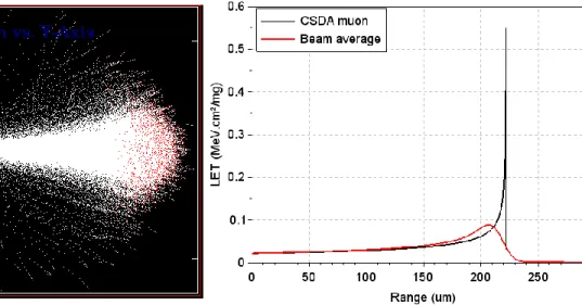
Radiation-matter interactions are stochastic in nature; two charged particles from the same accelerated beam, at the same initial energy and hitting the same target, will be affected differently by the target atoms. In particular, at low energy, nuclear scattering with different impact parameters (or off target atoms of different species) leads to a significant dispersion in the path of the incident particles. This dispersion in the particle paths creates a dispersion in their range (the depth at which a particle will stop in a target) called range straggling, which particularly affects light particles such as protons, muons and electrons. This means that different individual particles from a monoenergetic beam will likely experience their Bragg peak at different depths; the result is that the mean ionization created by a particle beam follows a curve with a smoother peak, called the Bragg curve [50]. Figure 10 shows the dispersion of a monoenergetic 2 MeV antimuon beam in a silicon target. Figure 11 compares the average ionization generated by a 2 MeV antimuon beam to the ionization generated by an antimuon which would behave according to the Continuous Slowing-Down Approximation (CSDA). This model assumes that the particle
Figure 10: Illustration of the lateral and longitudinal dispersion of a 2 MeV antimuon beam inside a silicon target. The beam enters the target from the left edge; trails of white dots indicate the paths of individual muons, and red dots indicate their final resting positions. The target is 260 μm deep. Source: SRIM.
Figure 11: Ionization generated / stopping force experienced by a CSDA antimuon (black curve), and average ionization generated by an antimuon beam (red curve). The CSDA antimuon curve illustrates that while individual particles may have a narrow Bragg peak, a beam has a smooth Bragg curve because of straggling. Source: Geant4, using the MRED code.
26
always experiences the average stopping force theoretically matching its energy, and travels along a straight path. Figure 11 illustrates the fact that the LET of a particle can vary by more than an order of magnitude over distances of a few micrometres, as it decelerates in a target.
Knowing the Bragg curve of a particle beam and its range dispersion in the target as a function of the beam energy is important when planning an irradiation campaign, to ensure an appropriate interpretation of the test results.
27
Chapter III – Memory devices
A. General principles
1) History
Memory components are ubiquitous in computer systems, where their function is to store data. Several different technologies may be used to manufacture memory components; in the early days of the computer, data storage was implemented with macroscopic devices which sometimes relied on mechanical action for their operation, such as core memories, delay line memories, magnetic tapes and hard drives. While the latter two technologies are still in use nowadays, the use of fragile mechanical parts creates reliability and performance issues, and for this reason they are progressively coming to obsolescence.
In the late 1960’s, new types of memory devices were developed, which do not rely on any mechanical parts for their operation, but instead are implemented on a single integrated circuit. These are called solid-state memories. Depending on their storage mechanism, solid-state memories can be divided into two categories:
• Volatile memories, which do not retain information if their power supply is disconnected. Volatile memory technologies generally produce fast and low-latency data storage, which makes them ideal as data caches and buffers in fast computer systems. However, this comes at the expense of high power consumption, and sometimes more complex operation and lower storage density/capacity. Examples of volatile memory technologies are Static Random-Access Memory3 (SRAM) and Dynamic Random-Access Memory (DRAM).
• Non-volatile memories, which retain the data if their power supply is disconnected. If the environmental conditions are right (temperature, electric and magnetic fields, etc.), the data can be retained over at least several decades; for this reason, they are often included in computer designs to be used as storage memory. Non-volatile memory technologies generally offer low (or zero) standby power consumption, high storage density and capacity at low costs per bit, while their common drawbacks are slow operation, high latency and relatively poor read/write endurance. Examples of non-volatile memory technologies are Electrically-Erasable Programmable Read-Only Memory (EEPROM) and flash memory.
The present study aims at studying the effects of radiation on solid-state memories exclusively. For convenience, in the rest of this document, the expressions “memory component”, “memory device” or “memory” will be used to refer to solid-state memories.
2) Memory architecture
Most solid-state memories share a similar architecture: they present a series of external connectors (called “leads”, “pins” or “pads” depending on their shape) which are used to operate it – typically an address bus, a data bus, control signals for read/write signalling, and sometimes a clock signal. At the heart of the component, connected to the external pins via bonding wires, is a piece of silicon called the
3 In Random-Access Memories (RAMs), the access latency does not depend on the order in which data are accessed.
This is the case for most solid-state memories, and is in contrast with electromechanical storage technologies such as hard disk drives or magnetic tapes, where a reading head must be positioned at the correct physical position on the storage medium to read the data.
28
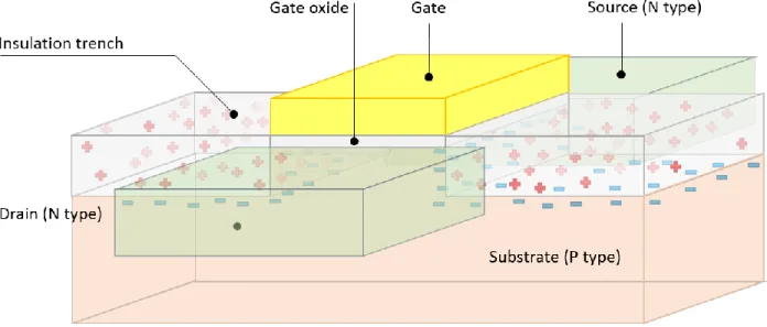
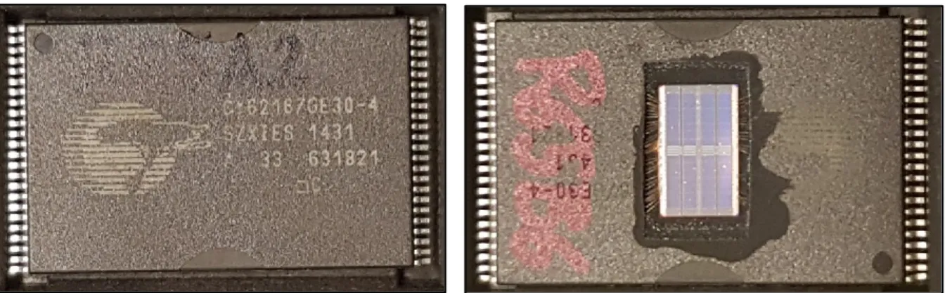
memory die, which is cut in a single silicon crystal. The connectors, bonding wires and memory die are encapsulated in a plastic or ceramic package. Embedded in the memory die is an integrated circuit, on which two regions can be defined:
• The memory array, in which the data is stored in a multitude of simple individual circuits called memory cells (generally only one bit is stored per cell). Each memory cell is made of one or more transistors, and sometimes other elements (e.g. a capacitor) depending on the technology. The cells are organized in rows and columns, along which run power supply, ground, control and data lines which connect the cells in parallel.
Traditionally, the term “word line” is used to designate the control lines running “horizontally” along the rows of the array, which are used to “select” the cells, while “bit line” is used to designate the control/data lines running “vertically” along the columns and connected to the cells’ inputs and outputs. However, these terms may vary from one technology to the other.
• The peripheral circuitry (or more simply, “the periphery”), which is located around the memory array and is used to access, write to and read from it. The periphery also regulates the memory array’s supply voltage. It is always implemented using CMOS technology4.
Depending on the technology, the output of a memory cell may be either a voltage level or a current level, which amplitude will depend on the cell’s logic state. To correctly evaluate this logic state, the output must be compared to a reference value. One possible solution is to embed reference voltage (or current) sources in the chip; this has the advantage of minimising the silicon area, but makes the system vulnerable to possible drifts in the output of the reference source (caused e.g. by temperature variations, accumulated dose, etc…). The system robustness to parametric shifts can be greatly enhanced by adopting a differential architecture, at the expense of doubling the area required by the memory array. In differential architectures, each single bit is stored in two separate half-cells, with one holding the actual bit and the other holding its complement; to read one bit, the two half-cells are read and their outputs are compared.
The physical storage location of a bit within the memory array depends on two factors:
• The address scrambling scheme, which attributes an address bit to each stage of the address decoder. There is no “standard” address scrambling scheme, and the information is typically not readily released by the manufacturer. This means that two words whose addresses are related (differ only by a few bits) might effectively be stored in very different regions of the die.
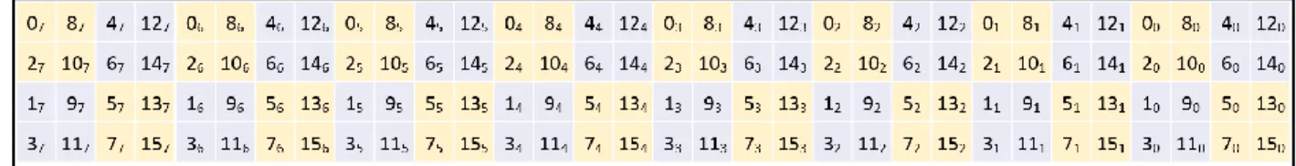
• The bit interleaving scheme. It is common for several words to be stored on the same row, in such a way that each word’s bits are distant from each other. Figure 12 illustrates how the bits (weights 7 to 0) of words A, B, C, D, E, F, G and H could be interleaved on a single row. Bit interleaving allows bits of similar weight to be placed next to each
4 Complementary Metal-Oxide-Semiconductor technology, or CMOS, refers to the practice of implementing logical
functions using both P-type and N-type field-effect transistors (MOSFETs), to form logically complementary structures. CMOS technology is the most popular technology for integrated circuit design, mainly because of its low static power consumption.
Figure 12: Illustration of an arbitrary bit interleaving scheme (bottom row) involving eight words A to H (color code on the top row).
29
other; this makes it easier to multiplex their associated bit lines into a single sense amplifier. Interleaving also brings a higher immunity to Multiple-Bit Upsets (MBU, see next chapter); a single particle is less likely to affect several bits of the same word if their memory cells are distant from each other.
3) Operation
To perform an operation on the memory, a command must be sent by setting its control inputs at specific values according to a pre-established timing. An access is made to the memory location designated on the component’s address bus: the periphery sets several transmission gates5 to electrically connect the control and data lines of the relevant memory cells to the periphery’s. The periphery decodes the command (typically “read” or “write”) and accordingly readies subsystems for the operation to come:
• for a “read” operation, the states of the accessed memory cells are determined. For example, in SRAMs, this is done by pre-charging all bit lines to a certain voltage, then selecting the row containing the relevant cells. The cells containing e.g. a logic ‘0’ will discharge their bit lines faster than the cells containing a logic ‘1’; after a short period, the voltages of the bit lines are evaluated by very sensitive analog circuits called sense amplifiers. This evaluation gives
the information stored in the memory cells; this information is stored in an output buffer, and output on the memory’s data bus.
• for a “write” operation, the bit lines are each set at ‘1’ or ‘0’ depending on the data to be written; then, the word containing the relevant memory cells is selected, and the data in these cells will be overwritten by the information stored on their bit lines.
The exact sequence of operations carried out on the control lines depends on the technology used to manufacture the memory cells, some of which will be reviewed in the next section.
5 A transmission gate is a CMOS circuit used to electrically connect or disconnect two signal lines. The transmission
gate has one control input, one data input and one data output. It is made of two transistors (one NMOS and one PMOS) connected in parallel to the two data terminals; both of their gates are connected to the control input, but one (e.g. the PMOS’ gate) is complemented by an inverter. When the control gate is at ‘1’, the PMOS can transmit high voltage levels to from the data input to the output, while the NMOS can transmit low voltage levels. If the control gate is at ‘0’, no voltage transmission can occur through either the PMOS or the NMOS, so the input and output are effectively disconnected.
Figure 13: Organization of an SRAM memory block's cells and peripheral circuitry. The same principles apply to most other memory technologies, although the number of bit lines and control lines may differ. Power supply and ground lines are omitted for clarity.