HAL Id: tel-00624418
https://tel.archives-ouvertes.fr/tel-00624418
Submitted on 16 Sep 2011HAL is a multi-disciplinary open access archive for the deposit and dissemination of sci-entific research documents, whether they are pub-lished or not. The documents may come from teaching and research institutions in France or abroad, or from public or private research centers.
L’archive ouverte pluridisciplinaire HAL, est destinée au dépôt et à la diffusion de documents scientifiques de niveau recherche, publiés ou non, émanant des établissements d’enseignement et de recherche français ou étrangers, des laboratoires publics ou privés.
eFPGAs : Architectural Explorations, System
Integration & a Visionary Industrial Survey of
Programmable Technologies
Syed Zahid Ahmed
To cite this version:
Syed Zahid Ahmed. eFPGAs : Architectural Explorations, System Integration & a Visionary Indus-trial Survey of Programmable Technologies. Micro and nanotechnologies/Microelectronics. Université Montpellier II - Sciences et Techniques du Languedoc, 2011. English. �tel-00624418�
- 1 -
Université Montpellier 2 (UM2)
École Doctorale I2S
LIRMM
(Laboratoire d'Informatique, de Robotique et de Microélectronique de Montpellier)Domain: Microelectronics
PhD thesis report for partial fulfillment of requirements of Doctorate degree of UM2
Thesis conducted in French Industrial PhD (CIFRE) framework between: Menta & LIRMM lab (Dec.2007 – Feb. 2011) in Montpellier, FRANCE
“
eFPGAs: Architectural Explorations, System Integration & a
Visionary Industrial Survey of Programmable Technologies
”
eFPGAs: Explorations architecturales, integration système, et une enquête visionnaire
industriel des technologies programmable
by
Syed Zahid AHMED
Presented and defended publically on: 22 June 2011
Jury:
Mr. Guy GOGNIAT Prof. at STICC/UBS (Lorient, FRANCE) President
Mr. Habib MEHREZ Prof. at LIP6/UPMC (Paris, FRANCE) Reviewer
Mr. Jürgen BECKER Prof. & CHEO at KIT (Karlsruhe, GERMANY) Reviewer Mr. Michael HÜBNER Senior Scientist at KIT (Karlsruhe, GERMANY) Examiner Mr. Laurent ROUGÉ Founder & CEO Menta (Montpellier, FRANCE)
Examiner/Co-Advisor Mr. Gilles SASSATELLI Research Director at LIRMM/CNRS FRANCE) (Montpellier, Co-Advisor Mr. Lionel TORRES Prof. at LIRMM/UM2 (Montpellier, FRANCE) Advisor
- 3 -
Short Abstracts in French & English as per requirements of UM2.
RÉSUMÉ
La thèse s'articule autour du thème des FPGA embarqués (eFPGAs). Ce manuscrit analyse les solutions existantes actuellement et discute les challenges et opportunités de ces technologies; une analyse en profondeur des échecs des tentatives passées est également donnée. Sur la base des solutions existantes dans la littérature, une structure de eFPGA à topologie de type grille est proposée, décrite en langage VHDL RTL. Cette solution comporte également les outils de programmation associés. Sur la base de cette proposition, des explorations sont menées quant à la pertinence des solutions proposées au sens de métriques d’actualité tells que densité logique, performance et consommation. Une des contributions notables de cette thèse repose sur la proposition d’une architecture de switch unifiée éliminant les blocs de connexions ainsi que l’interconnexion locale typique des FPGA actuels (telles que ceux modélisables dans le logiciel VPR) tout en autorisant une bonne routabilité. Toutes les expérimentations ont été menées sur une technologie CMOS 65nm faible puissance du fondeur STMicroelectronics, qui permet de fait d’obtenir des évaluations pertinentes. Une seconde contribution notable repose sur l’exploration de l’intégration de eFPGA dans un contexte système sur puce (SoC). Cette approche repose sur l’adjonction d’un eFPGA au sein d’un système intégré, au côté d’un processeur de type LEON3, la programmation s’effectuant sur la base d’une approche de type ESL. Deux explorations sont ainsi déclinées, comme unité intégrée au sein du processeur et comme coprocesseur. Les résultats présentés permettent ainsi d’analyser sous plusieurs angles les compromis possibles ainsi que les perspectives et limitations de ce type d’approches. Finalement, un cas d’étude est également présenté quant à l’intégration de mémoires de type magnétique (MRAM) au sein-même de l’architecture du eFPGA.
Mots-clés: architecture eFPGA, outils CAO pour eFPGAs, enquête industrielle, accélération reconfigurable, ESL, MRAM
ABSTRACT
The thesis extensively revolves around embedded FPGAs (eFPGAs). It conducts detailed survey focused on programmable technologies to investigate potentials and challenges of eFPGAs and probable failure reasons of several past attempts of different kinds. Based on the survey knowledge, technology independent soft eFPGAs of FPGA-like mesh-based classical architecture with standard RTL programming flow are investigated. Detailed eFPGA architectural explorations (including CAD tools) are conducted to explore silicon-efficient (logic density, power, performance etc.)eFPGA architectures. Among notable innovations achieved is unified switch block with complete removal of connection block and local interconnect of classical mesh-based FPGAs (VPR-like) while maintaining good routing efficiency. All experiments are conducted on 65nm CMOS low powerSTMicroelectronics process to get practical silicon values and perspectives. Finally eFPGAs in systems (SoCs) potentials and challenges are addressed. A reconfigurable acceleration scenario with ESL exploitation (for programming ease) and full silicon tradeoffs visualization is presented with integration of eFPGA with LEON3 processor (as a functional and co-processor unit, with also highlighting potential flaws of functional unit in industrial perspectives). An interesting case study for perspectives of emerging MRAM memories for eFPGAs is also presented.
Keywords: eFPGA architectures, CAD tools for eFPGAs, industrial survey, reconfigurable acceleration, ESL, MRAMs
- 4 -
ABSTRACT
(Extended)
Rising design complexities and high manufacturing costs of System on Chip (SoCs) in deep submicron nodes (beyond 90nm) have reached levels where dedicated SoCs can no longer be designed for every application. They must have some post manufacturing flexibility to amortize the high development costs to several end markets. The Field Programmable Gate Arrays (FPGAs) are well known for their flexibility and ease of design modification. With the continuous architectural innovations and Moore’s law they have become programmable platforms and in many cases provide a good alternative to implement SoCs directly on them. Unfortunately FPGAs suffer from large silicon gap compared to ASICs/ASSPs. This restricts their use in many high volume applications, and despite enormous benefits of flexibility FPGAs still represent a small niche in industry from revenues stand point compared to ASICs/ASSPs. An obvious choice that comes in mind in such scenario is embedded FPGAs (eFPGAs) to bring benefits of FPGAs right inside SoCs, bridging their challenges for flexibility, product differentiation, time to market etc. However concept of eFPGAs is not new to industry and is historically well known for never succeeding, despite undeniable benefits and potentials.
The thesis work extensively revolves around eFPGAs in three major themes. (i) Survey and analysis of programmable technologies to investigate scope, potential, challenges of eFPGAs. (ii) eFPGAs architectural explorations and tools infrastructure to create efficient customized eFPGAs. (iii) eFPGAs in SoCs investigations and perspectives (including beyond classical technologies/techniques). The general flow and aspects of discussions are as follows.
The thesis presents detailed investigations of FPGAs and eFPGAs research challenges by analyzing state of the art in industrial and academic research. It conducts detailed survey focused on programmable technologies to address potentials and challenges of eFPGAs and probable failure reasons of several past attempts of programmable solutions of different kinds. Based on the knowledge gained from detailed investigations, motivations and potentials of FPGA-like technology independent soft eFPGAs are presented. The CAD tools and graphical infrastructure to create and explore customized eFPGAs with standard RTL programming flow is presented. Detailed eFPGA architectural explorations are conducted to create efficient soft eFPGA architectures with attractive silicon properties (logic density, power, performance etc.). Among notable innovations achieved is complete removal of connection block and local interconnect of classical mesh-based FPGAs (VPR-like) while maintaining good routing efficiency by investigating unified switch block architecture with specialized diverse connectivity of logic block to unidirectional routing network. All experiments are conducted on CMOS 65nm low power STMicroelectronics (ST) process to get practical silicon values and perspectives. Finally eFPGAs in Systems (SoCs) potentials and challenges are addressed in detail. A case study of reconfigurable acceleration is presented with integration of eFPGA with LEON3 processor (as a functional unit and co-processor, with also highlighting flaws of functional unit from commercial stand point). Use of ESL is investigated for programming ease of eFPGA while maintaining standard RTL flow and complete silicon tradeoffs of the conducted experiments are investigated. To further enhance the potentials of eFPGAs for systems, investigations and perspectives of beyond classics emerging Magnetoresistive Random Access Memories (MRAMs) is also briefly discussed as an interesting case study.
Keywords:eFPGAs, FPGAs, CAD tools for eFPGAs, silicon analysis, survey of programmable technologies, FPGAs patents survey, SoC, reconfigurable computing, eFPGAs as co-processors, ESL, MRAMs for FPGAs
- 5 -
Acknowledgements
Finishing a PhD is a great moment of heterogeneous excitements. I thank God for helping me achieve this (my precious!) milestone in such serendipitous and adventurous ways that I have no doubt that treasure is indeed the journey itself. Acknowledgements are the easiest and hardest part of the thesis to write, one can easily write the whole acknowledgements section for almost all theses in just one simple sentence “I would like to thank my parents/family and above all the usual suspects (those of skill will understand anyways)”. But I prefer going the other way to well address and exploit the market share of acknowledgements for theses, so I begin my quest.
Parents: First and foremost my parents for their endless love. It’s been more than 7 years since I embarked on MS+PhD wonders to foreign lands (reminds me of 7 years of that infamous wizard boy of novels/movies, who ironically also finishes his quest on big screen in July 2011). Sometimes I visited my parents after up to two years of delay due to schedules/visa issues etc. They are my greatest asset. They will hardly understand my thesis at all, but indeed will have the highest joy knowing I did it, whatever it was!
Advisors: I like to thank my mentor Dr. Gilles Sassatelli: the man who brought me to France from Germany, perhaps the primary reason I did my PhD from LIRMM, donated me to Menta/Industry. Indeed he deserves the highest market share of credit for this thesis. My acquaintance with him stretches back to late 2004 when I attended his visiting block-lecture in TU-Darmstadt during my masters; it was there I got severely infected with virus of reconfigurable technologies in all forms (later was partly vaccinated by the industry) and was also the first time I programmed an FPGA. I would like to extend my deep regards to Prof. Lionel Torres: the supreme commander of this thesis, a born leader with multitude of research interests and strong eye on industry too. During a significant part of my thesis he was also serving as director of microelectronics department of LIRMM and I used to be fascinated observing his exceptional email skills to steer things. His continuous influence and advice to do stuff like: present this whole concept in 10 slides; explain this entire scenario in few lines etc. helped me practice such skills that were invaluable in making fine publications and also this thesis report. I will also like to deeply thank both Gilles and Lionel for: their everlasting patience for/to my industry vs academia hysteria (due to industrial PhD), my life time absence award presence in the lab, reviewing of my research papers to correct/transform their industrial sauce language to a form digestible by peer scientific reviewers (and they were, we almost never lost!). They also provided me opportunity to occasionally take part in conferences program committees that further helped me understand back-end of conferences, review process and also psychology of reviewers.
Menta: I would like to express my gratitude to Mr. Laurent Rougé, primarily for founding Menta or none of this would have happened! (see prologue). My stay at Menta was full of heterogeneous experiences, challenges and opportunities making my industrial PhD a true industrial PhD, helping me get trained as a student of industry (see epilogue). Being almost of my age Laurent was always more a close friend than boss. Other than our countless hours of technical/business discussions, he shared with me his enormous general knowledge and also provided me substantial knowledge about France. My research work would never had been possible without the help of my colleagues (and also several master thesis students that came along the way) at Menta (co-authors of my papers). I will always remember the wonderful time spent with Jean-Baptise Cuelle, Julien Eydoux and Alexandre Martheley, particularly our quest of eFPGA Creator. Finally I thank Menta as a whole; it was a pleasure to see/have my thesis a foundation part of it and hope it will help partly guide future strategies.
Jury: I would like to express deep regards to my distinguished jury members. Firstly thanks to Prof. Guy Gogniat for accepting being president of the jury, giving memorable final remarks on the thesis work on behalf of jury and announcing me Dr. I would like to thank Prof. Habib Mehrez for accepting to be reviewer of my thesis. Being a well renowned authority and one of the very few professors in France/Europe deeply involved in FPGA architecture research domain his presence in jury was like a LUT in FPGA. I am thankful for his wonderful remarks on architectural explorations but perhaps will especially cherish forever his appreciating remark on my relatively unusual chapter 2 in the light of CIFRE PhDs [5.11]. It was a privilege to get such remarks from a very senior professor like him with decades of experience. I will like to express my heartiest regards to Prof. Jürgen Becker: a world renowned authority on industrial-driven FPGA-based reconfigurable systems, premier conferences chair etc. for accepting to be the 2nd reviewer of the thesis on a very short notice and despite
his enormously busy schedule due to his additional admin responsibilities. I will always remember his enchanted mail from Washington DC to Frankfurt flight in which he sent confirmation to jury members that he will be delighted to serve as reviewer. I am thankful for his wonderful remarks on thesis report and appreciations of this thesis’s understanding of industrial scenarios and challenges. I like to express my gratitude to Dr. Michael Hübner (the infamous apprentice & colleague of J. Becker): an iconic expert of Xilinx FPGAs, reconfigurable systems, peer conferences chair etc. to accept serving as examiner in the jury. Together Jürgen and Michael in addition to making my jury international brought Germany in it, the country where I fell in love with microelectronics and programmable technologies. Finally I will like to express my regards to the jury for their admiration of the multidisciplinary contributions and efforts of this thesis.
- 6 - Academia: Perhaps the most interesting part of PhD training is conferences, providing chance to meet leading experts from around the world. It is indeed hard to go in the long list but I like to mention few with whom I had quite interesting discussions on FPGAs/broad spectrum of programmable technologies/academia etc. which were very helpful in my research. In alphabetical order: A. Agarwal
(MIT), K. Benkrid (U. Edinburgh), E. Cota (UFRGS), O.
Hammami (ENSTA), L. Lagadec (UBO), G. Lemieux (UBC), R.
Leupers (RWTH Aachen), F. Moraes (PUCRS), F. Morgan (NUIG),
M. Lubaszewski (UFRGS), K. Torki (CMP). I like to thank
Prof. R. Tessier (UMASS); detailed informal discussions on
his summer 2009 visit to LIRMM were highly interesting. He gave several details about FPGA research, USA academia, general tips about PhDs and publications & my infinite questions about J. Rose. I will also like to express gratitude to Prof. M. Robert (LIRMM), master of my masters!
for his general tips (particularly his remark ―too many slides kill slides‖) on making nice presentations and art of extra slides. I will also like to re-thank Prof. M. Glesner (TUD); I
could not have done this PhD without the foundation knowledge of microelectronics that I learned in his institute during my Masters. Finally I like to express my deepest regards to the two great professors who mesmerized me the most (technically and their visionary unconventional styles) in my PhD. Unfortunately I only electronically met them: Prof. Jonathan Rose (U. Toronto) & Prof. Reiner Hartenstein (U. Kaiserslautern). I can write an entire chapter on them but
have limited silicon budget for acknowledgements and indeed cannot exploit Moore’s law on font size for obvious
reasons! In short: immense thanks to J. Rose for his vision
of sharing his publications online with the community & the infamous VPR book. Countless thanks to R. Hartenstein for his amazing keynotes (drove me crazy), contributions to education, Linkedin relationship and not killing me for stealing ―visionary‖ from his keynotes and put it in my thesis title. I dedicate my FPL10 survey presentation [S-3b] (slides were fortunately published! as part of FPL’s 20th
birthday initiative) to them both in general and in particular slide 26 (education crisis) to R. Hartenstein.
Industry: The story of my PhD is incomplete without the hypothetical Director-X (Semiconductor Industry). Looking back now to my PhD in some ways I have to admit that my biggest challenges and troubles came from the industry and were also partly solved by the industry (and story still goes on I guess). Just on the mere 2nd day of my PhD I had to directly encounter the industry [S-2], it was a strange and sudden shock, things were too different than much softer academia and perhaps like a fairytale story I was instantly in a new world I had no idea of. However in that strange world I came across counterparts of our academian world, on the top of which is UBM (United Business Media) empire (owner of EEtimes and several other EEtimes-like electronic media) and also similar efforts of companies for teaching consumers, physical technology and business experts etc. It took a while before I reluctantly shook hand with this strange master as a student of industry and it took me to a free! magic carpet ride to this strange new world ―so hard to live in, so hard to leave‖. I guess now I have partly realized why we call it real-world. I am highly thankful to Director-X for all the trainings and skills, they were priceless to deal challenges of my PhD; I owe in particular my chapter 2.3 to him. Coming from hypothetical to real (the musketeers of Director-X), I would like to express my regards to some of the fascinating people from technology/business I came across in scientific/industrial conferences, discussions with them were highly rewarding in my thesis. In alphabetical order: V. Betz
(Altera), M. Dickinson (Altera), V. Kathail (Synfora), H. Kim (Samsung), H. Krupnova (ST), P. Kundu (Intel), P. Lysaght (Xilinx), G. Martin (Tensilica), M. Muller (ARM), HN.Nguyen (Bull), I.Phillips (ARM), G. Saucier (D&R), C. Schmitt (eSilicon), J.Tully
(Gartner)., H. Wildt (fenix-da). I will also like to express gratitude to the infamous industry bloggers in related domain, to name just few (in alphabetical order): P. Clarke (EEtimes), E. Esteve (SemiWiki), D. McGrath (EEtimes), D. Manners (EltectronicsWeekly), R. Merritt (EEtimes), C. Maxfield (EEtimes), D. Nenni (SemiWiki), R. Wilson (EDN), J. Yoshida (EEtimes). Their wonderful articles taught me a lot. Finally I thank EEtimes as a whole for its open and social structure, webinars, virtual conferences etc. I wish one day there is UBM-like UAM (United Academics Media).
Friends: There is nothing like friendship in the world. In the usual darkness, stress, frustrating moments during thesis it’s the loving friendships that come to rescue. It is near impossible for me to go in the details of all the friends in/out of Montpellier, France, Euorpe, World (haven’t met any alien yet!) and I am afraid I will hardly be able to do justice in mentioning names so I use a trick partly borrowed from what we do in research papers for author names. My dearest @facebook, @linkedin et al, you mean more to me than dead silicon and there is indeed lot more to life than research.
ANRT: Finally I like to thank ANRT/CIFRE [5.11] for providing me strong motivations and revenue for this phenomenal complex adventure to get trained for research and industry, which I frequently used to dub during my PhD as ―Industry vs Academics (|\/|): the inside story of my PhD (see epilogue!)‖. The ANRT’s ROI hopefully will be highly justified in years to come & I wish to be/remain a close friend of academia in industry.
- 7 -
“Ph deDicated to … Dreams of Grad Students”
Family
:In loving memory of my late grandfather, Syed M. Sami Ahmed (died in 2002) who always wished of me to become a Dr. of medicine (often termed the real Dr.), when I preferred and took Engineering he wondered if I become the other Dr. Now I guess/hope I shall be providing treatments to/for Sick-SoCs.
- 8 -
Table of Contents
ABSTRACT ... 4
PROLOGUE ... 17
CHAPTER 1: INTRODUCTION ... 18
1.1 Motivation & Objectives ... 18
1.2 Contributions ... 19
Survey & Analysis [R] ... 19
eFPGA Architectural Explorations [B] ... 20
eFPGA in Systems [G] ... 20
1.3 Thesis Organization ... 21
CHAPTER 2: SURVEY & INVESTIGATION OF OBJECTIVES [R] ... 23
2.1 FPGAs State of Art ... 23
2.1.1 FPGAs Fundamentals ... 24
2.1.2 FPGA vendors ... 27
1 The Logic Block ... 27
2 Routing Architecture ... 31
3 Architectural Heterogeneity ... 33
4 Post 90nm Challenges of Power vs. Performance ... 34
2.1.3 Academics ... 38
1 FPGA CAD ... 38
2 Architectural Research ... 42
2.1.4 Beyond Classics emerging works ... 44
Architecture ... 45
Configuration ... 45
2.2 Systems with embedded FPGAs (eFPGAs) ... 46
2.2.1 Industry ... 46
1 General overview ... 46
2 FPGAs2010 with Hard Processors (FPGA or eFPGA!) ... 48
2.2.2 Academics ... 49
1 FPGAlike embedded FPGAs ... 49
2 CoarseGrain Reconfigurable Architectures ... 51
2.3 The Semiconductor Industry ... 52
2.3.1 Understanding Industry in general ... 52
1 Industrial articles and press news (From IEEEtimes to EEtimes) ... 52
2 Patents study of State of the Art ... 52
2.3.2 Global overview of Industry ... 53
1 Semiconductor Industry markets and market leaders ... 53
-- 9 --
3 Challenges of Power Consumption ... 55
2.3.3 Types of Programmable Hardware ... 55
1 Highend MPSoCs ... 55
2 Heterogeneous MPSoC Platforms ... 55
3 FPGAs ... 55
4 Versus (vs) FPGAs (MPPAs, CoarseGrain, Structured ASICs etc.) ... 57
2.3.4 FPGAs and vs FPGAs ... 58
1 History of PLD startups ... 58
2 Dominance of FPGAs: Fundamental Pros & Cons ... 58
3 Survey of vs FPGAs companies ... 61
4 Why vs FPGAs mostly failed/fail ... 61
5 New FPGA startups, their differentiation ... 62
6 New Trends among top FPGA vendors ... 63
2.3.5 Industry is heading for Platform Collision ... 64
1 Cloudy Future ... 64
2 Is eFPGA a missing IP ... 65
2.4 Summary... 66
CHAPTER 3: CAD INFRASTRUCTURE OF EFPGA... 67
3.1 Architecture Fundamentals of eFPGA ... 68
3.1.1 Island style unidirectional routing Architecture... 68
3.1.2 Building Blocks of eFPGA ... 70
3.1.3 eFPGA Core... 71
3.2 eFPGA Programmer™: eFPGA Programming tools suite ... 71
3.2.1 Frontend ... 72
3.2.2 Backend ... 72
3.3 eFPGA Creator™: eFPGA Creation GUI tools suite ... 73
3.3.1 Motivations & General Overview ... 73
1 Two objectives: Creation of eFPGA, Exploration of eFPGA ... 73
2 Inspiration from VPR: ease of “whatif” experiments ... 73
3 Inspiration for GUI based tools: added user friendliness dimension ... 74
4 Global Overview of the tools suite ... 74
3.3.2 Library Manager (eFPGA components creation) ... 76
1 GUI Wizards & Editors ... 77
2 Hardware Generation ... 78
3.3.3 Architecture Manager (eFPGA Core creation) ... 80
1 GUI wizards & Editors ... 80
2 Hardware Generation ... 81
3 Architecture files generation ... 81
3.3.4 Analyzer (Design Space exploration) ... 83
1 Mapping, Clustering & Placement ... 84
2 SB & eLB ... 85
3 Global Routing ... 85
4 Silicon ... 87
-- 10 --
CHAPTER 4: EFPGA ARCHITECTURAL EXPLORATIONS [B] ... 89
4.1 Basic Explorations for General Overview ... 89
4.1.1 Experimentation Methodology ... 90
1 Experimentation flow and Benchmarks ... 90
2 Adaptable HDL of eFPGA: Silicon exploration ease ... 91
3 Basic GUI exploration tools ... 92
4.1.2 LUT Size ... 93
1 Mapping efficiency vs LUT Size ... 93
2 Silicon Exploration ... 95
4.1.3 Cluster and Channel ... 96
1 Channel width vs Cluster size ... 97
2 Silicon Exploration ... 97
3 Clustering Feedback analysis ... 99
4.1.4 Routing Analysis ... 100
1 Channel size challenges ... 100
2 Routing efficiency analysis ... 101
3 Tile traffic analysis ... 101
4 Hop Analysis ... 102
4.1.5 Challenges of Power Consumption ... 103
1 Area, Power, Speed comparison at 90, 65, 45nm nodes ... 103
2 Power vs Speed: effect of threshold voltage ... 104
4.1.6 Comparison with State of Art ... 105
4.2 Explorations with Tile Customization (eFPGA Creator) ... 107
4.2.1 Experimentation motivations and methodology ... 107
1 General motivations ... 107
2 Exploration objectives ... 108
3 CAD flow and Benchmarks ... 109
4.2.2 SBRouting Multiplexers optimization... 110
1 Custom Architecture types ... 110
2 Silicon Properties ... 111
3 Architectural analysis (benchmarks mapping) ... 111
4.2.3 SBeLB Interconnect Multiplexers optimization ... 117
1 Custom Architecture types ... 117
2 Silicon Properties ... 118
3 Architectural analysis (benchmarks mapping) ... 118
4.2.4 Combined optimizations and explorations ... 123
1 General Comparison with classical architecture ... 123
2 Combined experiments for SBR+SBeLB joint best cases ... 123
3 Effect of threshold and process node type (power vs speed) ... 125
4.2.5 Miscellaneous Experiments Perspectives ... 126
1 Feedbacks optimization ... 126
2 SB Topology (Diversity) and Flexibility ... 127
3 Effect of LUT and Cluster size ... 127
4 Explorations with Architectural Heterogeneity ... 127
-- 11 --
CHAPTER 5: EFPGA IN SYSTEMS [G] ... 129
5.1 General Motivations ... 129
5.1.1 eFPGAs potentials in SoCs ... 129
1 Product Differentiation, Time to market ... 129
2 SoC prototyping (testing new ideas) ... 129
3 Multiple possibilities (differentiation, experimentation, reconf. acceleration etc.) ... 130
4 Soft eFPGAs (technology independence) ... 131
5.1.2 eFPGAs as reconfigurable accelerators ... 131
1 Not new concept, mostly failed, why again ... 131
2 Standard RTL flow and rise of ESL tools ... 131
3 Out of Box thinking: use weakness as strength ... 132
4 Basic Experiments done with Two Processors (Plasma & LEON3) ... 132
5.2 eFPGA with LEON3 Processor ... 133
5.2.1 eFPGALEON3 System Integration ... 133
1 As a Functional Unit (processor pipeline) ... 133
2 As a CoProcessor Unit ... 133
5.2.2 Experimentation Flow ... 134
1 Application Profiling (HW/SW partitioning)... 134
2 Application mapping (use of ESL) ... 134
3 Analyze Silicon tradeoffs (Area, Power, Speed) ... 134
5.2.3 Experiment with AES algorithm... 136
1 Profiling AES ... 136
2 Mapping HW/SW partitioned portions on LEON3+eFPGA ... 136
3 Analyzing Silicon Tradeoffs at 65nm (Area, Power, Speed) ... 138
5.2.4 Benefits of ESL vs Optimal Hand coded HDL ... 141
5.3 System Integration Challenges ... 142
5.3.1 General overview ... 142
5.3.2 Basic experiments with AMBA ... 143
5.3.3 Processor inside FPGA vs FPGA inside Processor perspectives ... 143
5.4 MRAM based eFPGAs case study ... 145
5.4.1 MRAMs fundamentals ... 145
1 Working principle and Hybrid CMOS hardware ... 145
2 Types and Properties ... 146
5.4.2 Perspectives for eFPGAs ... 147
1 ReProgrammable NonVolatility ... 147
2 Radiation Hardness ... 147
3 Shadowed Dynamic Reconfiguration ... 147
4 MultiContext (with low silicon overhead) ... 148
5 Integration and Fabrication ease with conventional CMOS ... 148
Test Chips (MRAMs, Latch/SRAM based configuration) ... 150
MRAM based configuration Test Chips (ST130nm) ... 150
Latch/SRAM based configuration Test Chip (ST65nm) ... 151
-- 12 --
CHAPTER 6: CONCLUSIONS & FUTURE LINES OF RESEARCH ... 153
6.1 Conclusions ... 153 6.1.1 Summary of Contributions ... 153 6.1.2 Knowledge Gained ... 154 6.2 Future Directions ... 156 6.3 Concluding Remarks ... 157
EPILOGUE ... 158
APPENDIX... 159
A1: General overview/survey of FPGA vendors Patents ... 159
A2: Extended tables and discussions of Chapter 4 ... 165
A3: NoC+MRAM Perspectives for eFPGAs/eFPGAsbasedSystems ... 170
A4: Document Statistics ... 172
ABBREVIATIONS ... 173
PHD CONTRIBUTIONS ... 174
Panels ... 174
International Conferences ... 174
International Publications ... 174
BRIEF CV & CONTACT ... 175
REFERENCES ... 176
1 FPGA Vendors ... 176
2 Industry (General) ... 178
3 Patents of FPGA Vendors ... 180
4 Academics ... 185
5 Books & Others ... 190
-- 13 --
List of Figures
Fig. 1: Research Blocks Graph of thesis contributions 19
Fig. 2.1a: FPGA architecture fundamentals: Island Style Architecture [Betz&Rose99, 4.1] 26
Fig. 2.1b: FPGA architecture fundamentals: Uni/Bi directional routing [Lemieux04, 4.19] 26
Fig. 2.2: The logic blocks (equivalent) of Stratix III and Virtex 5 [Altera, 1.15] 28
Fig. 2.3: The SLICEM of Xilinx Virtex6 [Xilinx, 1.3] 28
Fig. 2.4: Building a LUT [Altera, 1.20] 29
Fig. 2.5: DelayCost Tradeoff with LUT Size [Altera, 1.20] 29
Fig. 2.6: The mapping efficiency of LUT6 [Altera, 1.20] 29
Fig. 2.7: The Detail of Altera StratixIV ALM [Altera, 1.14] 30
Fig. 2.8: Implementing 5 and 3 input functions on Altera ALM and Xilinx LUT6 [Altera, 1.20] 30
Fig 2.9: Global Architecture of Xilinx VirtexII [Xilinx, 1.8] 31
Fig. 2.10: Routing Architecture sides Altera (left), Xilinx (right) [Altera, 1.18] 31
Fig. 2.11: Hierarchical Routing Resources of VirtexII [Xilinx, 1.8] 32
Fig. 2.12: Logic Array Block (LAB) structure of Altera Stratix IV [Altera, 1.14] 33
Fig. 2.13: The routing HOP [Altera, 1.23]; {Note: source image is blurry!} 33
Fig. 2.14: Altera StratixIV block diagram [Altera, 1.14] 34
Fig. 2.15: Stratix IV architectural elements with columns of hard blocks [Altera, 1.14] 34
Fig. 2.16: Static & Dynamic Power vs Tech. Node [Xilinx, 1.7] 35
Fig. 2.17: The Components of leakage current [Altera, 1.16] 35
Fig. 2.18: The Leakage current Impact, sensitivity and Design techniques [Altera, 1.16] 35
Fig. 2.19: The transistor density scale factor [Xilinx, 1.4] 35
Fig. 2.20: Leakage Power vs Temperature in 90nm Virtex4 [Xilinx, 1.7] 36
Fig. 2.21: Programmable Power Technology of Altera through Quartus II [Altera, 1.16] 36
Fig. 2.22: Transistor type distribution in Virtex6 FPGAs for combating power [Xilinx, 1.4] 37
Fig. 2.23: The relative power consumption of Virtex FPGAs on different nodes [Xilinx, 1.4] 37
Fig. 2.24: Performance and Density Improvement in Stratix FPGAs on different nodes [Altera, 1.23] 37
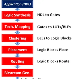
Fig. 2.25: Generic FPGA CAD flow [Betz&Rose99, 4.1] 38
Fig. 2.26: Fully Connected Clustered Logic Block [Betz&Rose99, 4.1] 39
Fig. 2.27: Modeling FPGA routing as a directed graph [4.10] 41
Fig. 2.28: Theme concept of eFPGA IP in SoC/ASIC/ASSP 46
Fig. 2.29: 90nm Morpheus Chip with eFPGA of Abound Logic/M2000 [2.28] 47
Fig. 2.30: Atmel CAP Microcontrollers with Metal Programmed (MP) embedded fabric [2.34] 47
Fig. 2.31: FPGAs with Hard ARM: Xilinx 28nm EPP and Actel 130nm Smart Fusion (source: web) 49
Fig. 2.32: Hardware comparison between standard custom FPGA (left) and Soft FPGA (right) [4.31] 50
Fig. 2.33: Directional (left) and Gradual (right) [4.31] 50
Fig. 2.34: Semiconductor industry 2009 (230 B$) markets and market leaders [S3b][2.1][2.15] 54
Fig. 2.35: Top FPGA/PLD vendors market share and revenues [2.14][2.20] 54
Fig. 2.36: Makimoto’s Wave: Cyclic nature of Industry (Source: open web) 54
Fig. 2.37: OMAP4 platform of TI (source: TI web) 56
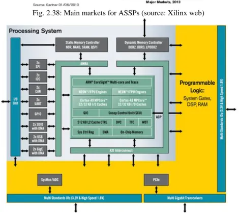
Fig. 2.38: Main markets for ASSPs (source: Xilinx web) 56
Fig. 2.39: Xilinx 28nm ZynqEPP devices (source: Xilinx web), {Note: source image is blurry!} 56
Fig. 2.40: MPPAs and Coarse Grain architecture styles 57
Fig. 2.41: History of Programmable Logic Device (PLD) startups 60
Fig. 2.42: Industrial survey of MPPAs and Coarse Grain companies [2.13] 61
Fig. 2.43: Industry is heading towards Platform Collision [S3b] 65
Fig. 3.1: Fundamentals of eFPGA Architecture 69
Fig. 3.2: Details of eFPGA architecture fundamentals 69
Fig. 3.3: Fundamentals of a classical Mesh architecture ([Betz&Rose99, 4.1]) for comparison 69
Fig. 3.4: Building blocks of eFPGA Architecture 70
-- 14 --
Fig. 3.6: eFPGA Creator Tools suite global overview 74
Fig. 3.7: Library Manager flow/overview 76
Fig. 3.8: Library Manager: library tree, components explorer 77
Fig. 3.9: Library Manager: some snapshots of editor GUIs 78
Fig. 3.10: Library Manager: Scripts generator 79
Fig. 3.11: Architecture Manager flow/overview 80
Fig. 3.12: Architecture manager 81
Fig. 3.13: eFPGA Creator Architecture Manager Snapshots 82
Fig. 3.14: eFPGA Creator Arch. Files generator 82
Fig. 3.15: eFPGA Creator Analyzer 83
Fig. 3.16: eFPGA Creator Analyzer GUI cockpit 84
Fig. 3.17: LUT mapping analyzer 84
Fig. 3.18: Clustering efficiency analyzer 85
Fig. 3.19: Placement analyzer 85
Fig. 3.20: SBeLB traffic analyzer 86
Fig. 3.21: Global routing analysis 86
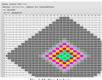
Fig. 3.22: Hop Analysis 87
Fig. 3.23: Tile Area distribution analysis 87
Fig 4.1a: Experimentation flow for basic explorations 90
Fig 4.1: Basic Hardware (Tile) of eFPGA Architecture 92
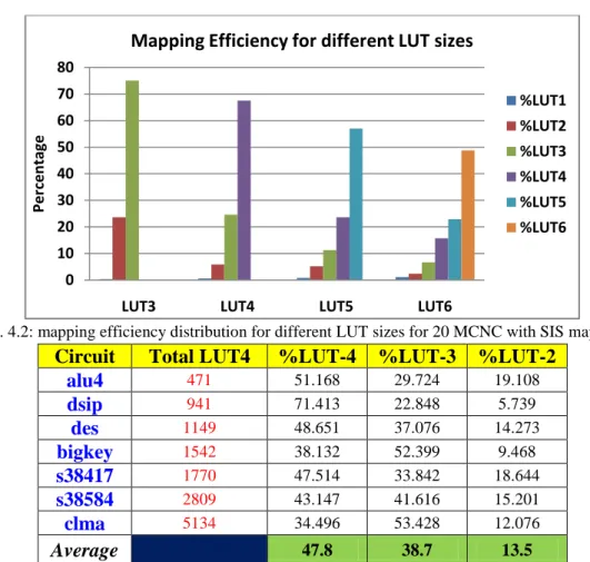
Fig. 4.2: mapping efficiency distribution for different LUT sizes for 20 MCNC with SIS mapping 94
Fig. 4.3: Total LUTs needed by 20 MCNC mapping for different LUT sizes, normalized to LUT4 95
Fig. 4.4: LUT size comparison for area efficiency 96
Fig. 4.5: Average Channel width (max) vs Cluster size for 20 MCNC 97
Fig. 4.6: Area comparisons for different cluster sizes 98
Fig. 4.7: Power comparisons for different cluster sizes and relative to cluster size 4 99
Fig. 4.8: Timing comparisons for different cluster sizes 99
Fig. 4.9: Average feedback statistics for different cluster sizes for 20 MCNC benchmarks 100
Fig. 4.10: Min. channel width requirement for different cluster sizes for benchmarks 101
Fig. 4.11: Routing efficiency analysis statistics 102
Fig. 4.12: Tile traffic analysis 102
Fig. 4.13: Routing Hop 103
Fig. 4.14: Hop Analysis 103
Fig. 4.15: Comparative Area, Power and Timing comparison on 90, 65 and 45nm 104
Fig. 4.16: Power vs Speed with different threshold voltages 104
Fig. 4.17: Hop Comparison of Virtex5 and StratixIII for inspiration 105
Fig. 4.18: The equivalent comparison of classical soft and soft eFPGA architecture 107
Fig. 4.19: The investigation objectives of SB customization 109
Fig. 4.20: The series of SBRouting mux customization 112
Fig. 4.21: Area breakdown for different SBR customizations 113
Fig. 4.22: Logic Density for different SBR customized architectures 113
Fig. 4.23: Average critical path delay of benchmarks for different SBR customizations 116
Fig. 4.24: Average routing statistics of benchmarks for different SBR customizations 116
Fig. 4.25: Silicon tradeoffs for different SBR customizations (*pessimistic power) 116
Fig. 4.26: The SBeLB multiplexers optimizations experiment custom architectures 119
Fig. 4.27: Area breakdown for different SBeLB customizations 120
Fig. 4.28: Logic Density for different SBeLB customized architectures 120
Fig. 4.29: Average critical path delay of benchmarks for different SBR customizations 122
Fig. 4.30: Average routing statistics of benchmarks for different SBeLB customizations 122
Fig. 4.31: Silicon tradeoffs for different SBeLB customizations (*pessimistic power) 122
Fig. 4.32: Architectural results comparison between classical (CB+LI) and unified SB eFPGA 123
-- 15 --
Fig. 4.34: Effect of threshold voltage and process type of same node on power 126
Fig. 4.35: Relative speedup for benchmarks for different ST65nm process node types 126
Fig. 5.1: Concept SoC scenario with eFPGAs 130
Fig. 5.2: eFPGA integration with LEON3 as functional unit and coprocessor 133
Fig. 5.3: Experimentation flow 135
Fig. 5.4: Profiling AES Application Critical function 135
Fig. 5.5: Profiling AES Application Critical function 137
Fig. 5.6: eFPGA resources for ESL vs Hand Coded VHDL 138
Fig. 5.7: LEON3+eFPGA silicon tradeoffs for different implementations 140
Fig. 5.8: Benefits of ESL compared to Hand coded HDL (Snapshots of Mentor’s Catapult) 141
Fig. 5.9: Basic experiments for eFPGA communicating with AMBA (AHB and APB) 143
Fig. 5.10: The trilogy of Reconfigurable Accelerators (problem of reconfigurable functional unit) 144
Fig. 5.11: Step sequences of TAS write operation in MTJ 146
Fig. 5.12: MRAM transistor level Hybrid CMOS circuit 146
Fig. 5.13: Basic Properties and types of MRAMs 146
Fig. 5.14: Perspectives of MRAMs for eFPGAs (the 5ive stars) 149
Fig. 5.15: MRAM based Shadowed Dynamic Reconfiguration 149
Fig. 5.16: MRAM based MultiContext configuration cell vs classical MultiContext cell 150
Fig. 5.17: MRAM integration and Fabrication with standard tools and standard CMOS 150
Fig. 5.18: MRAM 130nm small 4 LUT4 Test Chip (ST CMOS + Crocus MRAM) 151
Fig. 5.19: MRAM 130nm 1444 LUT4 FPGA Test Chip (ST CMOS + Crocus MRAM) 151
Fig. 5.20: ST65nm eFPGA Test Chip of Menta (64 LUT6) 151
Fig. 6.1: Innovation wheel for future research ideas 156
Fig. A2.1: Relative comparison of different LUT sizes with respect to LUT4 169
Fig. A3.1: Beyond Classics Routing Architecture potentials in/for eFPGA 171
-- 16 --
List of Tables
Table 4.1: 20 MCNC benchmarks, statistics with LUT4 mapping using SIS 91
Table 4.2: Mapping efficiency of different LUT sizes for 20 MCNC with SIS mapping 94
Table 4.3: Mapping efficiency of benchmarks on Virtex II Pro with Synplicity synthesis tool 94
Table 4.4: Percentage of LUTs area in total Tile area and mapping considerations 96
Table 4.5: Pessimistic Power of 150000 LUT6 eFPGA at different threshold voltages 106
Table 4.6: Selected benchmarks for tile customization experiments, mapped with eFPGA Programmer 109
Table 4.7: Silicon properties of 7 custom routing mux tiles for channel size 48 (*pessimistic power) 113
Table 4.8: PAR results for tile tsr_4448_F 114
Table 4.9: mapping results of tsr_4448 theme1 tiles 114
Table 4.10: mapping results of tsr_4448 theme2 tiles 114
Table 4.11: PAR results for tile tsr_4436_F 115
Table 4.12: mapping results of tsr_4436 theme1 tiles 115
Table 4.13: mapping results of tsr_4436 theme2 tiles 115
Table 4.14: Silicon properties of 7 custom SBeLB mux tiles for channel size 48 (*pessimistic power) 120
Table 4.15: PAR results for tile tse_4448_F 121
Table 4.16: mapping results of tse_4448 theme1 tiles 121
Table 4.17: mapping results of tse_4448 theme2 tiles 121
Table 4.18: Silicon statistics of best tile (*pessimistic power) 125
Table 5.1: Profiling of AES application 137
Table 5.2: Profiling of all C instructions in AES Code 137
Table 5.3: Different LEON3+eFPGA Implementation Steps 138
Table 5.4: eFPGA hardware resources for each step with ESL & Manual VHDL 138
Table 5.5: Area and Power consumption of LEON3 processor at 100MHz 139
Table 5.6: Pessimistic Power Statistics of 484 LUT6 eFPGA 139
Table 5.7: Performance gains with Silicon Tradeoffs 139
Table A2.1: Silicon statistics of SBR experimented tiles at LUT4, Cl4, Ch36 (*pessimistic) 166
Table A2.2: PAR statistics of base tile (_F topology) for decreasing channel width 166
Table A2.3: Silicon statistics of best case (SBR + SBeLB) hybrid tiles (*pessimistic) 166
Table A2.4: benchmarks PAR statistics for SBR+SBeLB theme 2 tiles 167
Table A2.5: benchmarks PAR statistics for SBR+SBeLB theme 3 tiles 167
Table A2.6: Silicon statistics of base tile for different LUT sizes (*pessimistic) 168
Table A2.7: benchmarks PAR statistics for base tile architecture (LUT6, LUT4) 168
Table A2.8: benchmarks PAR statistics for base tile architecture (LUT3, LUT5) 168
Table A2.9: Relative comparison of different LUT sizes 169
-Table A2.10: benchmarks PAR statistics of best SB-R+SB-eLB architecture for varied 65nm process types - 169 Table A4.1: Approximate Statistics of Thesis report 172
-- 17 --
Prologue
The origins of this thesis stretch back to the official founding of Menta in July 2007. When this thesis was created between Menta and LIRMM (University of Montpellier) under the umbrella of the CIFRE (in English: Industrial Contracts for training through Research) process of French Ministry of Higher Education and Research run by ANRT [5.11], the work started from December 2007. This created the first contracted employee/scientist for Menta and made the company from one man to the famous industry term ―two men in garage‖. Menta has matured and expanded over the years and at present (calendar Q2 2011) is the only known existing soft-eFPGA provider company.
The motivations and origins of this thesis work were very exciting and challenging. The long-term road map unknown, directions unknown, partners unknown, markets unknown, competitors almost unknown (in terms of existence), Industry soon entered into 2008-2009 global economic crisis. The almost known tagline was to make embedded FPGAs and ―everyone who tried to do this died or left the business‖. This thesis is not a Holy Grail for Menta, but indeed has tried to answer several questions and created some solutions. The startup nature of Menta, the economic crisis philosophical influence, the research knowledge of LIRMM, help from hypothetical Director-X (Semiconductor Industry, see acknowledgements section) with articles/blogs/press news/industrial events etc. along with several other factors (intent is providing perspective not autobiography) combined and created an almost ideal CIFRE PhD scenario which has theme motivation ―You will become a doctor once you
have defended your thesis, proving that you are capable of undertaking a substantial R&D project. You will be recognized for your participation in research and innovation, your keen capacity for tackling the problems facing a company, interaction with partners from different cultures. You will learn how to deal with the real-life situations your company faces, and acquire behavioral and interpersonal skills in the process‖ [5.11]. This
thesis report is the connection of dots looking backwards to the knowledge gained.
- 18 -
Chapter 1: Introduction
This chapter presents the global overview, motivations and contributions of this thesis work. Section 1.1 provides the challenges that are currently faced by industry in scenario of this thesis and what observations can be drawn from them for research motivations and objectives. Section 1.2 describes the major contributions of the thesis work and finally section 1.3 provides the outline of the thesis report.
1.1 Motivation & Objectives
Rising design complexities and high manufacturing costs of System on Chip (SoCs) have reached levels where dedicated SoCs can no longer be designed for every application. They must have some post manufacturing flexibility to amortize the high development costs to several end markets [S-1]. The Field Programmable Gate Arrays (FPGAs) are well known for their flexibility and ease of design modification. With the continuous architectural innovations and Moore’s law they have become programmable platforms and in many cases provide a good alternative to implement SoCs directly on them. However FPGAs suffer from large silicon gap in terms of Area, Power and Speed [Kuon&Rose09, 5.2] compared to ASICs (Application Specific Integrated Circuits), ASSPs (Application Specific Standard Products). This restricts their use in many high volume applications despite enormous benefits of flexibility. Although FPGAs being a steadily growing market, still represents just about only 2% of the semiconductor industry and as of 2009 represents around 4 billion dollars market compared to more than 80 billion dollars market of ASICs and ASSPs [2.1][S-3b].
However as stated above, it is becoming more and more essential for SoCs to have some post manufacturing flexibility for addressing key issues like product differentiation, time to market etc. With an added challenge of power consumption, that has become most crucial issue in industry and forcing the SoC designs to be more and more heterogeneous and customized to be optimal in power budgets. This gives dual challenge to SoC designers. On one side the flexibility is required to meet tough market challenges and on the other side solutions should be as custom and non-flexible as possible to meet silicon budgets.
An obvious choice that comes in mind in such scenario is embedded FPGAs (eFPGAs). eFPGAs allow bringing the well known FPGA benefits right inside the SoCs. However immediate question regarding eFPGAs is, how sound that idea is from technological and commercial perspective as the concept of eFPGAs is not new and well known in industry for never succeeding. What are the challenges and reasons that might have been the reasons of failures in the past and what can be learned from them as inspiration to avoid doing same mistakes. The goal and challenge for the SoCs is to seek some flexibility by having some programmable portions or IPs. FPGAs are most famous and dominant symbol of programmable devices but are not the only programmable devices. These challenges and observations lead to different questions and investigation motivations for eFPGA research, for instance.
What is the semiconductor industry landscape and how different technologies fit in it?
What are different types of competing programmable logic solutions? How they compare, what is their status and what are ongoing trends in industry and academic research?
Are FPGAs dominant in programmable logic space, if yes what makes them dominant?
Several efforts and innovative solutions in terms of programmable logic and reconfigurable computing have failed in past, what could be the reason and what can be learned from that?
Should eFPGAs follow FPGA-like conventional architecture, if yes what are the pros and cons? How to create eFPGAs effectively? What lessons and motivations can be learned from the past? How sound eFPGAs concept is for SoCs? What are the challenges, opportunities and perspectives? Can some beyond classics emerging works/technologies help to solve/improve some classical
- 19 -
Based on such diverse rough motivations and challenges the thesis contributed in several topics, which finally led to three main axes of contribution that are discussed below.
1.2 Contributions
The contributions of thesis are graphically illustrated in figure 1. The thesis extensively revolves around eFPGAs, to investigate and address the objectives of the thesis; the research done can be divided into three major blocks or axes. They are represented as Red [R], Blue [B] and Green [G] in the figure. Brief details of contribution areas of figure 1 are explained below.
Fig. 1: Research Blocks Graph of thesis contributions
Survey & Analysis [R]
The R axis acts as an umbrella covering the motivations and research directions, helping make well informed research decisions in the light of survey knowledge. It fundamentally addresses following aspects.
Study of state of art FPGAs in detail (literature, patents etc.) to find research challenges
Study of changing technological trends and challenges in industry (state of state of art) to get informed and trained for real-life challenges
Analyze potentials of different programmable technologies, inspect how/where eFPGAs fit in the spectrum and investigate the causes of failures of several past solutions in research and industry
This axis partly covers the obligatory part of almost all theses (analyzing basics of the state of the art in that area), with additional emphasis on survey of industrial solutions to well categorize and understand real-life challenges of/for eFPGAs and other programmable technologies in a broad spectrum.
Key Contributions:
In depth study of literature of leading FPGA vendors (research/commercial articles, patents etc.). Detailed study of academic research on FPGAs
Investigation of eFPGA/eFPGA-like efforts, solutions from industry and academics, visualizing probable reasons of past failures
Comprehensive survey of semiconductor industry, focused on programmable technologies with investigation of strengths and weaknesses (including failures of past) of different solutions
- 20 -
eFPGA Architectural Explorations [B]
The B axis extensively deals for the research of eFPGA architecture to create efficient customized eFPGAs, it is the biggest contribution axis of this thesis work in terms of efforts done and time spent. It fundamentally addresses.
Architectural explorations and innovations using FPGA CAD and silicon investigations to create efficient FPGA-like (LUT-based) technology independent soft eFPGAs
Focus on beyond CMOS 90nm nodes (65nm was mostly used) to visualize static power challenges Compare and tune architectures to be more area, power, timing efficient for benchmarks applications Create tools infrastructure to facilitate and accelerate research investigations
This axis is similar to classical FPGA architectural research. It deals with architectural innovations with the CAD and silicon visualizations of the architectures on advanced nodes (beyond 90nm for judging issues of leakage etc.) of real silicon process by implementing the architecture and analyzing the silicon properties of those architectures in terms of area, power and performance. Numerous tools were created to facilitate the exploration research. This axis performs combined CAD and silicon investigation for understanding the pros and cons of the under investigation architectures in terms of architectural efficiency (mapping benchmark applications) and silicon efficiency (logic density, speed, power). Qualifying both is essential; architecture must succeed implementing benchmarks to qualify for the chosen architectural parameters (LUT size, cluster size, channel size, routing architecture etc.) to be appropriate for the target domain for which eFPGA is being created, and on the other hand the proposed architecture must have attractive silicon properties in terms of area, power and performance to be value added proposition for the end product (SoC, ASSP, ASIC etc).
Key Contributions:
Exploration of unified SB (switch block) based architecture with eliminated local interconnect (LI) of logic block which is found in CB (connection block) based VPR-like architectures [4.1] Soft technology independent architecture (multiplexer based routing, latch/flip-flop based
configuration) with unidirectional/single-driver routing architecture
eFPGA Creator™: tools suite to create and explore customized eFPGAs. This thesis contributed
Motivations for advanced GUI based tools infrastructure for exploration
Full/partial design of several portions of the tools suite for custom architectures exploration Automatic hardware generation (VHDL and scripts) of custom architectures
Detailed analysis of fundamental architectural parameters (LUT size, cluster size, channel size etc.) on STMicroelectronics CMOS 65nmLP process for benchmark applications (MCNC [4.1]) for general overview
Exploration of connection of logic block to the routing architecture (through unified SB) in depopulated diverse ways to highly enhance silicon efficiency (rivals past published results) Exploring power vs speed issues and challenges with change of threshold voltage (LVT, SVT,
HVT) and process node type (LP, GP) on STMicroelectronics CMOS 65nm
eFPGA in Systems [G]
Since the thesis work is focused on embedded FPGAs, the G axis investigates the challenges and opportunities (from knowledge of R axis) of eFPGAs in systems scenario. It fundamentally addresses. eFPGAs in SoC scenario as an IP
eFPGAs as reconfigurable accelerator
System integration challenges (in terms of physical integration, and value addition vs silicon tradeoff) Investigation of perspectives of beyond classics technologies/methods for enhancing eFPGAs
- 21 -
The work and knowledge of B and G axes are highly interlinked. B quests for creating efficient eFPGAs and G visualizes how efficient they will be in some real scenarios. The philosophy behind the eFPGA of Menta is to create soft target independent customized eFPGAs programmable by standard flows for everybody and suitable for multiple potentials as seen in the concept system diagram with eFPGAs in figure 1. This axis investigates the potentials and challenges related to that in general and in detail the potentials of reconfigurable acceleration. It also highlights and investigates the perspectives of beyond classics emerging technologies to help solve some conventional problems and enhance eFPGAs potentials.
Key Contributions:
General discussions for potentials of eFPGAs for industry, reconfigurable computing (reconfigurable acceleration with standard RTL programming flow with ESL exploitation)
eFPGA interfacing with processors (as functional unit and co-processor unit), perform experiments (HW/SW co-design) with full silicon tradeoffs visualization on ST 65nmLP
Highlighting in industrial scenario: ESL benefits, potential flaws of reconfigurable functional unit, system integration challenges and issues for eFPGAs
A real and innovative case study for the potentials of beyond classics emerging MRAMs for enhancing eFPGAs capabilities (non-volatility, dynamic reconfiguration, multi-context, fabrication ease etc.), an interesting compliment for the eFPGA research work of this thesis
1.3 Thesis Organization
The thesis is organized in a suitable way to address the ideas, contributions and easier for the reader to understand. In addition the chapters are clusters of mini chapters to further elaborate the exact distinct objective of the chapter based on figure 1, which leads to three distinct chapters (with CAD infrastructure presented as separate chapter for ease of discussions). Furthermore all sections and subsections of the chapters in most cases are further characterized to effectively present the center ideas immediately for the reader. The outline of the chapters is as follows.
Chapter2 details the contribution R of the thesis work. The chapter itself is composed of the three fundamental axes of the thesis [RBG] divided in three core sections. Section 2.1 outlines research challenges of FPGAs, as eFPGA has a classical LUT based architecture so understanding the FPGA challenges is obligatory. This section covers these aspects in detail in both industrial and academic scenario. Section 2.2 addresses the issues and work done with embedded FPGAs, which is essential for this thesis as it deals with embedded FPGAs so additional challenges regarding eFPGAs must be understood. Finally section 2.3 details the industrial survey and will address the major findings of the commercial research. It presents general overview of industry and its markets; survey focused on programmable technologies highlighting their strengths and weaknesses and finally investigates how/where eFPGAs fit in the spectrum of current changing trends in the industry.
Chapter3 is an overview chapter of the CAD infrastructure of eFPGAs (partly and closely related to axis B
contribution). It provides the fundamentals of eFPGA architecture, its programming flow and tools which program it and then in detail the eFPGA Creator with its user friendly graphical tools suite which helps to create customized eFPGA architectures. It will provide a comprehensive overview of the motivations, differentiations of the tool and its capabilities to create, analyze and implement customized eFPGAs, and contributions of this thesis work in that regard.
Chapter4 addresses the research contribution B in detail which is the largest contribution of this thesis work in terms of time spent and experiments conducted. It describes the detailed experiments conducted for eFPGA architectural exploration in the light of knowledge gained from chapter 2 and with the help of eFPGA Creator (chapter 3). Section 4.1 presents general experiments to understand and investigate several
- 22 -
fundamental research challenges with FPGAs. Later sections detail architectural research done using eFPGA Creator for creating complex customized architectures which have higher density, higher speed and lower power compared to basic customized architectures of section 4.1 while still being capable of efficiently routing benchmark applications. All experiments are fully analyzed on ST65nm low power process for area, power and speed tradeoffs.
Chapter5 presents the research contribution G. Section 5.1 provides general motivations and potentials of eFPGAs for SoCs, in particular as a reconfigurable accelerator. Section 5.2 presents detailed experiments conducted with eFPGAs and LEON3 integration. Section 5.3 outlines the system integration challenges in the light of industrial survey and experiments knowledge of the thesis. Finally the chapter presents the case study of using MRAMs (Magnetoresistive RAM) based eFPGAs in SoCs. It also briefly outlines the test chips that were taped out based on eFPGA architecture explored by this thesis (130nm MRAM based configuration test chip, 65nm latch/SRAM based configuration test chip).
Chapter6 provides the conclusions and future outlook.
References section is characterized and partitioned, it can also serve as a partial standalone chapter role. The citation of references in text is done with numerical reference (section.ref number) and sometimes additional information is augmented with the numerical reference for added ease of reading in context. The form used in general is [AuthorYear, ref.] or [Company_AuthorYear, ref.]. Self citations have the form [S- number]. This creates a customized domain specific solution, combining benefits of several styles often used in citations.
Disclaimer/Notice
Tools created in the thesis work are property of Menta. The name of the tools (eFPGA Programmer, eFPGA Creator, FPGA Designer, Niagara etc.), the design flows, name of eFPGA components (eCB, eLB, eAB, ePB, eMB etc.) are copyrights of Menta. This report must not be considered or treated as any current, future product/plan or business strategy, roadmap of Menta.
- 23 -
Chapter 2: Survey & Investigation
of Objectives [
R
]
The first step of research is to analyze the state of the art in that area and the contributions done by other researchers. This chapter discusses deeper investigations of the three foundation axes (RBG) of this thesis work explained in chapter 1.
Section 2.1 explains the fundamentals of FPGA architectures and
challenges. First it explains the architecture fundamentals and explain them in the light of advances in the state of the art including the post 90nm silicon challenges that are becoming the biggest challenge to all semiconductor industry in general so understanding these challenges is obligatory as wrong research conclusions or directions can easily be made if not effectively considering them. The research of FPGAs is virtually impossible without FPGA CAD tools, so understanding the fundamentals of them is essential. In this regard FPGA CAD research done by highest cited academics is discussed along with architectural challenges addressed by several academic works. Recent trends have shown that to meet the FPGA challenges research has also been conducted in beyond classics technologies, a brief overview of these approaches will be discussed and among them MRAMs and their potentials in bit more detail in this regard, which is one of complimentary contributing part of this thesis work in terms of beyond classics perspectives.
Section 2.2 discusses the embedded FPGA/embedded FPGA like solutions. In this regard very few success stories exist in industry, it will try to identify those approaches with their pros and cons. In principle more efforts are done in this area by academics than industry in different dimensions, it will present brief overview of these efforts in general and more relevant to this thesis work area in particular to find research motivations.
Section 2.3 addresses a differentiating part of this thesis work which serves as the foundation basis of the research directions and motivations. It will briefly discuss the efforts for understanding and integrating in industry, a survey of patents study of FPGA vendors, a comprehensive overview of semiconductor industry markets and a survey of programmable technologies in technical and especially commercial scenario.
2.1 FPGAs State of Art
The section first provides the almost vendor independent basic fundamentals of FPGA architecture and then comprehensively surveys the architectural enhancements and challenges addressed by state of art FPGA vendors and academics research (separately addressed for more clearly identifying their contributions) to find research challenges and motivations. Finally it also addresses an overview of some beyond classics researches underway in industry and academics (like MEMS, NoCs, MRAMs etc.) to investigate their potentials for solving some FPGA challenges. The outline is as follows.
Section 2.1.1 provides the fundamentals of FPGA architecture and terminologies which are not standard (all vendors use their own commercial names) but quite well known and recognized among research community to identify the research target. This section will help to understand later more advanced sections and also the research work conducted in this thesis.
Section 2.1.2 addresses the key advancements of the state of the art FPGAs through the years and latest new challenges in addition to fundamental ones due to growing issues of power consumption in beyond
- 24 -
90nm era. The thesis has considered mostly Xilinx and Altera in discussions as they are the market leaders with more than 80% market share [Coudert09, 2.10] and are most advanced in technology.
Section 2.1.3 will present several well recognized/cited research efforts from academics to address several key challenges of FPGAs architecture, in particular FPGA CAD. This further gives the insight to research challenges in addition to general overview from the state of the art research from section 2.1.2.
Section 2.1.4 will briefly address research efforts in industry and academics to use beyond classic technologies (MEMS, MRAMs, NoC etc.) to address some of the key challenges of FPGAs. We will concentrate bit more on MRAMs which have been used in close partnership in this work to conduct some beyond classics experiments. They will be further addressed in more detail in chapter 5.
2.1.1 FPGAs Fundamentals
Field Programmable Gate Arrays (FPGAs) have greatly evolved since their invention and commercialization in late 1980s ([Xilinx_Freeman89, 3.1]) and have become complex programmable platforms. However the fundamentals have remained similar. This section provides a brief overview of the fundamentals of FPGA architecture in vendor independent manner to highlight the key issues of architecture and terminologies that are widely common among scientific literature. They will help to grasp the main ideas quickly and will help in later discussions of other researches (industrial and academic) and explanations of this thesis work in later chapters. All FPGA vendors have their own commercial names for these fundamental elements and architecture styles that differentiate one from the other.
In a nutshell the foundation of FPGA can be described as a composition of three elements. First a logic block which has the Look-Up Table (LUT) to implement Boolean functions, paired with a Flip-Flop (FF) providing sequential behavior. The logic block is often composed of multiple LUT-FF pairs (logic elements) and usually referred as cluster in scientific literature. Second the programmable interconnect/routing architecture connects these clusters to route data. The third element is programmable I/Os which provide access to outside world.. The programming of FPGAs is mostly done by HDLs like standard ASIC flows of synthesis, place & route (PAR), and final step of bit/configuration generation makes FPGAs different than ASICs (CAD flow will be addressed in detail in section 2.1.3). The details of above mentioned architectural fundamentals along with some additional details are described below with the help of figure 2.1a and 2.1b.
Island Style/Mesh based Architecture
Figure 2.1a shows the generic block diagram of mesh based FPGA architecture [Betz&Rose99, 4.1]. The topology is often referred as ―Island Style‖ architecture in the literature where the logic blocks are surrounded by a sea of routing resources (connection block, switch block and routing channels) as shown in figure. The Island Style topology is the most widely used FPGA topology and is common among all leading FPGA vendors. The other less common topology is Hierarchical/Tree based (will be briefly addressed in section 2.1.3). This thesis work is also based on Island Style architecture. A brief detail of building blocks of the architecture is discussed below.
Logic Block/Cluster
The logic block (LB) is the main computational element of an FPGA that provides the fine-grained reconfigurable flexibility of an FPGA. In principle it is a Look-Up Table (LUT) + Flip-Flop (FF) block that implements combinational/sequential Boolean logic of the mapped application. The LUT + FF pair is frequently referred as a logic element (LE) or a basic logic element (BLE) in the literature. The logic block can be a single BLE, but in practice is often composed of multiple BLEs and is called a cluster in literature and cluster size is an important architectural parameter which describes how many BLEs are in a logic
![Fig. 2.8: Implementing 5 and 3 input functions on Altera ALM and Xilinx LUT6 [Altera, 1.20]](https://thumb-eu.123doks.com/thumbv2/123doknet/7700455.245523/31.893.201.691.734.1072/fig-implementing-input-functions-altera-alm-xilinx-altera.webp)
![Fig. 2.15: Stratix IV architectural elements with columns of hard blocks [Altera, 1.14]](https://thumb-eu.123doks.com/thumbv2/123doknet/7700455.245523/35.893.139.757.538.794/fig-stratix-architectural-elements-columns-hard-blocks-altera.webp)
![Fig. 2.22: Transistor type distribution in Virtex-6 FPGAs for combating power [Xilinx, 1.4]](https://thumb-eu.123doks.com/thumbv2/123doknet/7700455.245523/38.893.257.639.107.357/fig-transistor-distribution-virtex-fpgas-combating-power-xilinx.webp)
![Fig. 2.29: 90nm Morpheus Chip with eFPGA of Abound Logic/M2000 [2.28]](https://thumb-eu.123doks.com/thumbv2/123doknet/7700455.245523/48.893.127.767.108.331/fig-nm-morpheus-chip-efpga-abound-logic-m.webp)