HAL Id: tel-01807927
https://tel.archives-ouvertes.fr/tel-01807927
Submitted on 5 Jun 2018
HAL is a multi-disciplinary open access archive for the deposit and dissemination of sci-entific research documents, whether they are pub-lished or not. The documents may come from teaching and research institutions in France or abroad, or from public or private research centers.
L’archive ouverte pluridisciplinaire HAL, est destinée au dépôt et à la diffusion de documents scientifiques de niveau recherche, publiés ou non, émanant des établissements d’enseignement et de recherche français ou étrangers, des laboratoires publics ou privés.
Imran Wali
To cite this version:
Imran Wali. Circuit and system fault tolerance techniques. Electronics. Université Montpellier, 2016. English. �NNT : 2016MONTT313�. �tel-01807927�
Délivré par l’Université de Montpellier
Préparée au sein de l’école doctorale I2S
Et de l’unité de recherche LIRMM
Spécialité: SYAM
Présentée par Imran WALI
Circuit and System
Fault Tolerance Techniques
Soutenue le 30 Mars 2016, devant le jury composé de:
M. Fabrice MONTEIRO, Professeur, Université de Lorraine Rapporteur Mme. Lirida NAVINER, Professeur, Telecom ParisTech Rapporteur M. Matteo SONZA REORDA, Professeur, Politecnico di Torino Examinateur M. Alberto BOSIO, MCF HDR, Université de Montpellier Examinateur M. Arnaud VIRAZEL, MCF HDR, Université de Montpellier Directeur de thèse M. Patrick GIRARD, DR CNRS, LIRMM CoDirecteur de thèse
Acknowledgements
First and foremost, I would like to thank my Lord, the Almighty, for being close and responsive throughout the course of my thesis. Only due to His countless gifts of sense, intellect, patience, health, family and many more, I could complete this task.
I would like to express my deepest gratitude to my thesis director, Prof. Arnaud Virazel. With his encouraging and supporting attitude, meeting him has always been a work-stress reliever for me. His profound guidance and invaluable advises helped keeping my research well directed and my progress on schedule while maintaining my autonomy.
My sincere thanks also goes to my co-director, Prof Patrick Girard, for his immense knowledge, motivation and support throughout the research. Also for his thought-provoking ideas and helpful criticism in improving the quality of this manuscript and other publications. I also appreciate Prof. Alberto Bosio’s insightful comments and advises which helped me solve various problems during my research.
My grateful thanks are also extended to Prof. Matteo Sonza Reorda for his generous support and effort to actively maintain the collaborative partnership, LAFISI, and his valuable and constructive suggestions that helped me enrich my ideas.
I am also thankful to him for carefully reviewing my work at different stages of my thesis. I would like to thank the rest of my thesis committee members, Prof. Lirida Naviner and Prof. Fabrice Monteiro for reviewing this manuscript and providing positive feedback.
I would also like to acknowledge all my master students who provided me an opportunity to enrich my understanding through sharing my knowledge about the subject and also for their valuable contribution to my work. I wish to acknowledge the support received form my friends at LIRMM for the various discussions and brain storming sessions. Also for making the last three years memorable.
Finally, none of this would have been possible without the love and patience of my family. Their constant support and strength has aided and encouraged me throughout this endeavor.
Abstract
Semiconductor is one of the most reliable inventions when engineered and used with longevity in mind. However, the increasing demand of fast and highly featured products has drastically changed the reliability realm in the recent years. The means of improving the reliability of nano-metric technology circuits encompass techniques that tackle reliability issues at the level of technology, design and manufacturing. Absolutely necessary but these techniques are almost inevitably imperfect. Therefore, it becomes essential to reduce the consequence of the "remaining" faults using fault tolerance techniques.
This thesis focuses on improving and developing new low-power fault tolerance techniques that combine the attractive features of different types of redundancies to tackle permanent and transient faults and addresses the problem of error detection and confinement in modern microprocessor cores. Our case study implementation results show that a power saving of up to 20% can be achieved in comparison with fault tolerance techniques that use only one type of redundancy, and offer lifetime reliability improvement.
With the objective to further improve the efficiency in terms of cost and fault tolerance ca-pability we present a design space exploration and an efficient cost-reliability trade-off analysis methodology to selectively harden logic circuits using hybrid fault tolerant techniques. The outcome of the two studies establish that hybrid fault tolerant approaches provide a good foun-dation for building low-power reliable circuits and systems from future technologies, and our experimental results set a good starting point for further innovative research in this area.
List of Acronyms
TMR Triple Modular Redundancy . . . xii
DMR Dual Modular Redundancy . . . 31
DVS Dynamic Voltage Scaling . . . 29
DFS Dynamic Frequency Scaling . . . 29
HyFT Hybrid Fault Tolerant . . . xiii
PHyFT Pipelined Hybrid Fault Tolerant . . . 51
HyTFT Hybrid Transient Fault Tolerant . . . xii
HyTPFT Hybrid Transient and Permanent Fault Tolerant . . . xii
BL Baseline . . . xii
PaS Pair-and-A-Spare . . . xv
FD Fault-Detection . . . 28
CL Combinational Logic . . . xii
SET Single Event Transient . . . 1
SEU Single Event Upset . . . 1
ID Instruction Decode . . . 64
IF Instruction Fetch . . . 64
EXE Execution . . . 64
MEM Memory . . . 64
WB Write-back . . . 64
STA Static Timing Analysis . . . 45
RTL Register Transfer Level . . . 67
HyFT-1a Original HyFT . . . xiii
HyFT-1b Hybrid Fault Tolerant (HyFT) Architecture with short DC . . . xiii
HyFT-2a Hybrid Fault Tolerant (HyFT) Architecture with CLK enclosed DC . . . xiii
HyFT-2b Hybrid Fault Tolerant (HyFT) Architecture with DC across CLK edge . . . xiii
ATPG Automatic Test Pattern Generator . . . 88
CMOS Complementary Metal-Oxide-Semiconductor . . . 9
SER Soft Error Rate . . . 1
SDF Standard Delay Format . . . 38
ix
DOR Dynamic OR . . . xv
FSM Finite State Machine . . . xvii
PaS Pair-and-A-Spare . . . xv
SoC System on Chip . . . 20
MTF Multiple Transient Fault MET Multiple Event Transient SPRA Signal Probability Reliability Analysis MEPP Multiple Event Probability Propagation BDD Binary Decision Diagram . . . 102
VF Vulnerability Factor SEE Single Event Effect . . . 1
FPGA Field-Programmable Gate Array . . . 120
Table of contents
List of figures xv
List of tables xix
Introduction 1
1 Context and Motivation 5
1.1 Semiconductor Technology Evolution . . . 5
1.2 Reliability threats in nano-metric technologies . . . 7
1.2.1 Variability . . . 7
1.2.2 Manufacturing Defects . . . 8
1.2.3 Wear-out . . . 8
1.2.4 Interference . . . 8
1.3 Errors in Integrated Circuits . . . 9
1.3.1 Soft Errors . . . 9
1.3.2 Hard Errors . . . 12
1.3.3 Timing Errors . . . 13
1.4 Reliability Improvement Approaches . . . 13
1.4.1 Fault Avoidance . . . 13
1.4.2 Fault Removal . . . 14
1.4.3 Fault Tolerance . . . 14
1.4.4 Fault Evasion . . . 15
1.5 Research Objectives . . . 16
2 Fault Tolerant Architectures and Assessment Techniques 19 2.1 Fault-Tolerance Techniques . . . 20
2.1.1 Concurrent Error Detection . . . 20
2.2 Fault tolerant Architectures . . . 28 2.2.1 Pair-and-A-Spare . . . 28 2.2.2 Razor . . . 28 2.2.3 STEM . . . 29 2.2.4 CPipe . . . 30 2.2.5 TMR . . . 30 2.2.6 DARA-TMR . . . 31
2.2.7 Hybrid Fault-Tolerant Architecture . . . 32
2.3 Robustness Assessment Techniques . . . 35
2.3.1 Axiomatic Methods . . . 35
2.3.2 Empirical Methods . . . 37
2.3.3 A Gate-Level Fault Injection Framework . . . 38
2.4 Experimental Comparative Study . . . 42
2.4.1 Experimental Methodology . . . 42
2.4.2 Comparative Analysis . . . 43
2.5 Summary . . . 48
3 Pipelined Hybrid Fault Tolerant Architecture 51 3.1 Error Propagation in Pipelined Circuits . . . 51
3.1.1 Linear Pipeline . . . 52
3.1.2 Nonlinear Pipeline . . . 53
3.1.3 Pipeline with Memory Interface . . . 53
3.2 Extension of HyFT Architecture to Pipelined Structures . . . 54
3.2.1 Basic Pipeline Cascading . . . 54
3.2.2 Stage/Combinational Logic (CL) Classification and Partitioning . . . 56
3.2.3 Dealing with Error Propagation in Nonlinear Pipeline . . . 59
3.2.4 Error detection in Pipeline stages with memory interface . . . 59
3.3 Case Study: Fault Tolerant Microprocessor . . . 63
3.3.1 Baseline (BL) Microprocessor . . . 64
3.3.2 Hybrid Transient Fault Tolerant (HyTFT) Microprocessor . . . 65
3.3.3 Hybrid Transient and Permanent Fault Tolerant (HyTPFT) Microprocessor 66 3.3.4 Triple Modular Redundancy (TMR)-b Microprocessor . . . 67
3.3.5 TMR-w Microprocessor . . . 67
3.3.6 Experimental Results . . . 67
3.3.7 Discussion . . . 78
Table of contents xiii
4 Design Space Exploration and Optimization of HyFT Architecture 81
4.1 Limitations of Hybrid Fault Tolerant (HyFT) Architecture . . . 81
4.1.1 Contamination delay constraints . . . 81
4.1.2 Asymmetric clock duty-cycle . . . 82
4.2 Design and Timing Optimization . . . 82
4.2.1 Original HyFT (HyFT-1a) Architecture . . . 83
4.2.2 Hybrid Fault Tolerant (HyFT) Architecture with short DC (HyFT-1b) . . 83
4.2.3 Hybrid Fault Tolerant (HyFT) Architecture with CLK enclosed DC (HyFT-2a) . . . 83
4.2.4 Hybrid Fault Tolerant (HyFT) Architecture with DC across CLK edge (HyFT-2b) . . . 85
4.3 Experimental Assessment of Improvements . . . 86
4.3.1 Experimental Setup . . . 86
4.3.2 Experimental Results . . . 92
4.3.3 Discussion . . . 97
4.4 Impact of circuit size on the evaluated metrics . . . 98
4.5 Summary . . . 99
5 Selective Hybrid Fault Tolerance 101 5.1 Previous work . . . 102
5.2 A low-cost output susceptibility analysis . . . 104
5.2.1 Results . . . 106
5.3 Validation of the approach . . . 107
5.3.1 Fault injection based output susceptibility analysis . . . 107
5.3.2 Discussion . . . 108
5.4 Selective HyTFT Architecture . . . 108
5.4.1 A low-cost HyTFT architectural reliability estimation . . . 110
5.5 Experimental Validation and Results . . . 112
5.5.1 Experimental Setup . . . 112 5.5.2 Experimental Results . . . 115 5.5.3 Discussion . . . 116 5.6 Summary . . . 116 Conclusion 119 Scientific Contributions 123
References 125
Appendix A HyFT Control Logic 133
Appendix B Workload Program 137
List of figures
1.1 Feature size and operating voltage scaling trend over years [22] . . . 6
1.2 Transistor count and clock frequency scaling trend over years [77] . . . 6
1.3 Single Event Effect Mechanism [9] . . . 10
1.4 Reliability improvement approaches across fault-failure life cycle [17] . . . 14
1.5 Error occurrences in combinational logic and storage elements . . . 16
2.1 Duplication with Comparison . . . 21
2.2 Duplication with Comparison in sequential logic circuits . . . 22
2.3 An static comparator with Error Latching mechanism moved upstream . . . 23
2.4 Pseudo-dynamic Comparator [93] . . . 24
2.5 4-input Dynamic OR (DOR) gate [93] . . . 25
2.6 Error detection architecture using the pseudo-dynamic comparator [93] . . . 25
2.7 General architecture of Error Detection with Codes [63] . . . 26
2.8 Examples of Rollback recovery schemes . . . 27
2.9 Principle of Pair-and-A-Spare (PaS) redundancy . . . 29
2.10 RAZOR Architecture [29] . . . 29
2.11 STEM Architecture [5] . . . 30
2.12 CPipe Architecture [89] . . . 31
2.13 Triple Modular Redundancy . . . 31
2.14 DARA-TMR [108] . . . 32
2.15 HyFT Architecture and associated timing constraints . . . 33
2.16 Error detection and correction in HyFT Architecture . . . 36
2.17 Fault Injection Flow . . . 38
2.18 Timeline illustration of Fault Injection Campaigns . . . 41
2.19 Impact of CL blocks size on area and power overheads . . . 45
3.1 Example transient error propagation in Linear Pipeline . . . 52
3.3 Example transient error propagation in Pipeline with Memory Interface . . . 55
3.4 Pipelined HyFT Architecture . . . 56
3.5 False error flagging . . . 57
3.6 Additional logic to prevent false error flagging . . . 57
3.7 False error flagging problem solved . . . 58
3.8 CL Classification and Partitioning . . . 58
3.9 Error detection and reconfiguration scheme in non-linear pipeline . . . 60
3.10 HyFT hardening of pipeline stage with asynchronous non-concurrent read-write access memory. . . 61
3.11 HyFT hardening of pipeline stage with synchronous simultaneous read-write access memory. . . 63
3.12 Baseline Microprocessor . . . 65
3.13 HyTFT Microprocessor . . . 65
3.14 HyTPFT Microprocessor . . . 67
3.15 TMR-b and TMR-w Microprocessor . . . 68
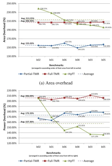
3.16 Area overhead results summary . . . 72
3.17 Power overhead results summary . . . 74
3.18 Transient fault injection results . . . 75
3.19 Permanent fault injection results . . . 76
3.20 Timing fault injection results . . . 76
4.1 Comparison-windowGeneration Circuits and delays . . . 84
4.2 Comparison-windowTiming Simulation Graph . . . 85
4.3 Modified Hybrid Fault Tolerant (HyFT) . . . 86
4.4 HyFT-1b Control Logic submodule1 . . . 89
4.5 HyFT-1b Control Logic submodule1 simulation . . . 89
4.6 HyFT-2a Control Logic submodule1 . . . 90
4.7 HyFT-2a Control Logic submodule1 simulation . . . 90
4.8 HyFT-2b Control Logic submodule1 . . . 91
4.9 HyFT-2b Control Logic submodule1 simulation . . . 91
4.10 Spatial distribution of Fail-silent faults . . . 95
4.11 Design metrics improvement summary . . . 98
4.12 Impact of circuit size on evaluated metrics . . . 99
5.1 Application of the output susceptibility analysis on an example circuit . . . 106
List of figures xvii
5.3 Output failure distribution . . . 108
5.4 Comparison of output susceptibility results (of CL block extracted form b05) . . 109
5.5 Selective HyTFT Architecture . . . 109
5.6 Cumulative weight calculation of an example circuit . . . 112
5.7 Selective HyTFT cost versus soft-error (of CL block extracted form b05) . . . 117
A.1 HyFT Control Logic . . . 133
A.2 HyFT Control Logic submodule1 . . . 135
A.3 HyFT Control Logic submodule1 simulation . . . 135
List of tables
2.1 Fault injection parameters . . . 39
2.2 Fault injection parameters . . . 43
2.3 Average Area and Power estimation results . . . 44
2.4 Transient fault injection results summary . . . 46
2.5 Transient fault injection results . . . 46
2.6 Permanent fault injection results . . . 47
2.7 Summary of comparison of different related fault-tolerant architectures . . . 50
3.1 Truth table . . . 57
3.2 Area and power results of write-transparency dual-port memory . . . 62
3.3 Baseline microprocessor specifications . . . 64
3.4 Fault injection parameters . . . 68
3.5 Area overhead results . . . 70
3.6 Power overhead results . . . 73
4.1 Contamination delay constraints for CL synthesis . . . 87
4.2 CL Synthesis Results . . . 88
4.3 Area Savings . . . 92
4.4 Power Savings . . . 93
4.5 Fault injection parameters . . . 94
4.6 Fault Injection Results . . . 96
5.1 Summary of selected previous work in the area of selective hardening . . . 103
5.2 Fault Injection Parameters for output susceptibility analysis . . . 107
5.3 Area, power and reliability estimates of Selective HyTFT variants . . . 113
A.1 HyFT submodule1 control signals . . . 134
Introduction
Technology scaling allows realization of more and more complex system on a single chip. This high level of integration leads to increased current and power densities and causes early device and interconnect wear-out. It leads to shifts in electrical characteristics of circuit elements or renders them permanently damaged. Moreover, a high integration density makes these complex systems difficult to test and some test-escaped manufacturing defects are encountered as errors only during infield operation. In addition, there are failures not caused by wear-out nor escaped manufacturing defects, but due to increased susceptibility of transistors to high energy particles from atmosphere or from within the packaging. Devices operating at reduced supply voltages are more prone to charge related phenomenon caused by high-energy particle strikes referred to as Single Event Effect (SEE). They experience particle-induced voltage transients called Single Event Transient (SET) or particle-induced bit-flips in memory elements also known as Single Event Upset (SEU).
High-performance microprocessors being at the forefront of technology are becoming in-creasingly vulnerable to hard and soft errors due to their growing complexity, high operating frequencies and fragility of future Very Large Scale Integration (VLSI) technology nodes. SEE in CL are playing important role in increasing Soft Error Rate (SER), which was historically considered as a cause of particle strikes in memory elements. In addition, it is estimated that the susceptibility of CL circuits to SET nearly doubles as the technology scales from 45nm to 16nm. Hence, it is inevitable for the industry to prevent reliability from becoming a bottleneck for the development of high-performance and low-power microprocessors.
The means of improving the reliability of nano-metric technology circuits encompass tech-niques that tackle reliability issues at the level of technology, design and manufacturing. Ab-solutely necessary but these techniques are almost inevitably imperfect. Therefore, it becomes essential to reduce the consequence of the "remaining" faults using fault tolerance techniques. These techniques employ information, timing and hardware redundancies to guarantee correct operations despite the presence of faults.
Various solutions using fault tolerant techniques for robustness improvement can be found in the literature, but a very few can address tolerance to both transient and permanent faults. These techniques generally rely on slow recovery mechanisms, thus are not suitable for highly interactive applications. For example, the method presented in [62] has little area overhead but runs Built-In Self-Test (BIST) during periodic time intervals to detect the presence of permanent faults and uses deep rollbacks that have a severe impact on performance. Fault-tolerant architectures like Razor [29], CPipe [89] and STEM [5] incorporate power saving and performance enhancement mechanisms like Dynamic Frequency Scaling (DFS) and Dynamic Voltage Scaling (DVS) to operate circuits beyond their worst-case limits. These architectures generally target timing errors and are not effective to deal with permanent faults. For instance, Razor only deals with timing faults and CPipe duplicates CL blocks in the pipeline to detect and correct transient and timing errors and can also detect permanent faults, but it does not offer provision for their correction.
Besides fault tolerance capability, power consumption is also a rising concern in the industry. In fact, as fault-tolerance becomes necessary in mass products, limiting power consumption of these techniques is one of the key factors in digital design. The classical fault tolerance techniques like TMR can effectively handle transient and permanent fault but cannot respect the low-power consumption demands.
Pipelining is a key technique to increase throughput in modern microprocessors by improving the resource utilization. But the complexity of interactions between pipeline stages make error detection and correction a major hurdle in designing high-performance reliable processing cores. To the best of our knowledge, none of the fault tolerance techniques in the literature address the problem of error detection and confinement in non-linear pipelined circuits nor in pipelines with memory interfaces.
Selecting the ideal trade-off between reliability and cost associated with a fault tolerant architecture generally involves an extensive design space exploration. Employing state-of-the-art reliability estimation methods makes this exploration unscalable with the design complexity.
This thesis focuses on improving and developing new low-power fault tolerance techniques that combine the attractive features of different types of redundancies for robustness improvement of future technology-scalable digital circuits and systems against transient and permanent faults. It addresses the problem of error correction in CL parts of complex pipeline circuits. Furthermore, it develops a fault tolerance capability assessment framework and low-cost reliability estimation techniques for use in cost-reliability trade-off analysis. Overall, this thesis establishes that hybrid fault tolerant approaches provide a good foundation for building low-power reliable circuits and systems from future technologies, and our experimental results set a good starting point for further innovative research in this area.
Introduction 3
• Chapter 1 details the context and motivation of our research. It starts with a discussion of the trends in semiconductor technology scaling and their impact on the reliability of nano-metric technology circuits. Later in Chapter 1 we briefly discuss the different approaches to improve their reliability and finally we end the discussion by presenting the objectives of our work.
• Chapter 2 covers the state-of-the-art in the field of fault tolerant architectures and robustness assessment techniques. It discusses some basic concepts of error detection and correction, followed by an overview of a set of state-of-the-art fault tolerant architectures, with a special focus on a hybrid fault tolerant architecture. In Section 2.3 we first develop the context by discussing some state-of-the-art methods employed for robustness assessment of circuits and systems and then present a gate-level fault injection framework for fault tolerance capability assessment of digital circuits. The last part of Chapter 2 presents an experimental study that quantitatively compare different fault tolerant architectures on the basis of their area, power, performance and their fault tolerance capability.
• In Chapter 3 we present a hybrid fault tolerant architecture for reliability improvement of complex pipelined circuits. We start the discussion by highlighting some issues that hinder error detection and correction in complex pipelined circuits. Then we discuss the extension of hybrid fault tolerant architecture discussed in Chapter 2 to make it solve the aforementioned problems. An experimental case study of the application of the developed fault tolerant architecture and other state-of-the-art solutions on a pipelined microprocessor is presented and finally with a comparative analysis we conclude the chapter.
• Chapter 4 consist of a design space exploration study aimed to optimize the cost and fault tolerance capability of the proposed hybrid fault tolerant architecture. We experimentally assess three proposed design improvements and present the results. The chapter is concluded by identifying the best candidate.
• Chapter 5 develops the principles of a low-cost reliability estimation method and a selective hybrid fault tolerant architecture. It starts with an overview of previous work in the area of selective hardening. In the subsequent sections we propose an efficient susceptibility analysis method to identify the most vulnerable circuit nodes for hardening and use it yo se-lectively harden some benchmark circuits. Also based on the susceptibility analysis method we also present a low-cost reliability estimation technique for fault tolerant architectures that use logic replication. In Section 5.5 we present the experimental result that compare the merits of circuits hardened to different extents and validate the hypothesis of the low-cost reliability estimation methods.
The Conclusion section summarizes the contributions of this work and presents some future perspectives.
Chapter 1
Context and Motivation
1.1
Semiconductor Technology Evolution
The steady growth of the global semiconductor industry over the past four decades has been driven by the demand for enhancing performance and functionality at reduced cost. This growth has been primarily facilitated by the continuous evaluation of semiconductor manufacturing technology. Transistors are scaled in each successive technology generation to increase their speed, improve packing density [2], decrease their power consumption and reduce cost. Thus, semiconductor technology scaling optimizes circuit performance and power consumption and allows realization of more and more complex system.
In November 1971, Intel introduced the world’s first single-chip microprocessor, the Intel 4004. It had 2,300 transistors, ran at a clock speed of up to 740 KHz, and delivered 60,000 instructions per second while dissipating 0.5 watts. The following four decades witnessed exponential growth in compute power, a trend that has enabled applications as diverse as climate modeling, protein folding, electronic games and autonomous soft landings on extraterrestrial bodies.
Today’s microprocessor chips employ billions of transistors, include multiple processor cores on a single silicon die, run at clock speeds measured in gigahertz, and deliver more than 4 million times the performance of the original 4004 [22]. The plots of Figures 1.1 and 1.2 show the trend of some technologic advancements in microprocessors in the past four decades. In 2015, Oracle presented the processor with over 10 billion transistors on the die, the most denser microprocessor in terms of transistor count. The major contributions to this massive advancement in semiconductor technology come from the field of lithography, advanced materials in manufacturing [70] and Electronic Design Automation (EDA) tools.
To reduce power dissipation of semiconductor devices, the supply voltage Vdd is also scaled,
Intel 4004 Intel 8086 Pentium Pro IBM POWER4 IBM POWER7 0.1 1 10 100 0.01 0.1 1 10 100 1965 1975 1985 1995 2005 2015 2025 T yp ical Oper a ting V o lt ag e (V) Minimu m F ea tu re Siz e ( µm) Year
Minimum Feature Size (μm) Typical Operating Voltage (V)
Fig. 1.1: Feature size and operating voltage scaling trend over years [22]
Intel 4004
Intel 8088
Intel 80486
AMD K7 AMD K10 18-core Xeon Haswell-E5
-4000 -2000 0 2000 4000 6000 8000 10000 1 10 100 1000 10000 100000 1000000 10000000 100000000 1965 1975 1985 1995 2005 2015 2025 F er q u ency (MHz) T ransis to r C o u n t (Thousan d s) Year
Transistor Count (Thousands) Frequency (MHz)
Fig. 1.2: Transistor count and clock frequency scaling trend over years [77]
to Vdd. However, voltage scaling only started in the late 80s because the industry had settled on
5V supplies in the early 70s to be compatible with bipolar Transistor-Transistor Logic (TTL) [21].
As power dissipation became unsustainable, this standard finally collapsed. Vddwas scaled within
few years, first to 3.3V then to 2.5V, etc. In 2011, supply voltage of high-performance ICs was at 0.9V and predicted to be reduced to 0.66V in 2021 [46].
In Figure 1.2 we can see that in year 2005, the frequency scaling process reached the power wall limit at about 3 GHz. In fact, higher switching activity of transistors leads to higher power consumption. Even though these small transistors do not consume much, hundred millions of them are switching at the same time in less than five hundred millimeter square IC. This results in significant power density that must be limited to avoid breakdown of physical materials.
1.2 Reliability threats in nano-metric technologies 7
The manufacturing cost has also played an important role in the evolution of semiconductor technology. Building smaller physical structures demand more sophisticated thus expensive equipment. But this initial investment makes little difference in per wafer cost in view of the sheer production size of new high performance, enhanced featured and low-powered integrated circuits, that always remain in high demand.
1.2
Reliability threats in nano-metric technologies
While offering many advantages technological trends into the nanometer regime have lead to a host of reliability issues. The sources that affect the reliability of modern circuits and systems are wide spread including manufacturing process variations, manufacturing defects, wear-out and interference. In the following sections we discuss how these reliability impairment sources evolve with technology scaling.
1.2.1
Variability
Variability of transistor characteristics due to variations in Process, Voltage and Temperature (PVT) have always been an issue in integrated circuit design [105]. PVT variations prevent the circuit from functioning correctly even though each individual transistor behaves correctly [71]. As device scaling enters into the nano-metric regime the effect of PVT variations are becoming more and more pronounced. Manufacturing process variations are increased due to the lack of precise control on the fabrication processes at small-feature technologies. They causes deviation of transistor characteristics and the resulting wide distribution leads to lower parametric yield [11].
Supply voltage scaling brings it close to or even below the transistor threshold voltage (Vth) to
achieve significant gains in energy efficiency. Once the supply voltage is lower than Vththe delay
shows an exponential dependence on the supply voltage, and therefore the magnitude of supply voltage shifts can have a significant impact on circuit delay [16, 82]. Scaling also gives rise to chip power densities and inadequate heat sinking cause hot spots to appear. These fluctuations of ambient temperatures alter the timing characteristics of circuits [51].
A conventional approach to deal with the problem of variability is to introduce large voltage and frequency guard-bands which considerably impact the power consumption and performance, cannot respond to rapid environmental changes [23] and implies a sharp increase in chip cost. Effectively dealing with variability to maintain or improve the high performance and energy efficient systems while satisfying the historical standards for reliability is becoming increasingly challenging with the scaling of technology [80].
1.2.2
Manufacturing Defects
Semiconductor manufacturing process may induce permanent defects in a chip during one or more of hundreds of process steps involving implantation, etching, deposition, polarization, cleaning and lithography [46] due to imperfections. The device miniaturization is making advanced technology devices nodes increasing vulnerable to these manufacturing irregularities. It is important that the testing be thorough as possible to uncover defective chips before they are shipped out [73]. However, according to past microprocessor data, the die size remains relatively constant [44], whereas the number of transistors per chip double every 2 to 3 years. This means that defect densities continues to increase. Moreover technology scaling and increasing complexity give rise to defects more subtle and difficult to detect [81, 84]. All these factors when combined with aggressive time-to-market objectives cause test escapes and raise reliability concerns.
1.2.3
Wear-out
As we have seen in Figure 1.1, the area scaling has had an exponential rate but the supply
voltage (Vdd) scaling has been quite slow. The two main reasons for slow Vdd scaling are to
keep up with the competitive frequency growth and to retain the basic noise immunity and cell stability [88]. Hence the dissimilar area and supply voltage scaling rates result in high power densities and elevated temperatures. The four well known wear-out failure mechanisms namely Time-Dependent Dielectric Breakdown (TDDB), Electromigration, Thermal Cycling and stress migration are all adversely affected by increase in temperature. These age-related hard errors that appear in-field after a certain period of use are major factors impairing the life-time reliability of modern microprocessors [87] used in data centers and space equipment. These applications demand high throughput and better lifetime reliability. However, these wear-out failures limit their useful lifetime and performance.
1.2.4
Interference
Beyond manufacturing defects and wear-out related permanent faults, integrated systems of recent years are more susceptible to temporary effects like transient or intermittent faults. These effects may be due to electromagnetic influences, alpha-particle radiation or cosmic radiations. They are the major portion of digital system malfunctions, and have been found to account for more than 90% of the total maintenance expense [79]. Smaller geometries increase coupling capacitances amount interconnects and current densities and cause problems of crosstalk. In
1.3 Errors in Integrated Circuits 9
nodes more susceptible to transient faults due to high energy particle from environment or from within the packaging.
1.3
Errors in Integrated Circuits
A fault, when active, is the cause of an error. An error is that part of the system’s state that may cause a subsequent failure, and a failure occurs when an error reaches the service interface and alters the service [7]. An error in integrated circuit can be classified according to its temporal characteristics [52], the product life-cycle stage of its induction, its severity etc. In the following subsections however we classify errors on the basis of their underlying faults, as this classification forms the basis of techniques to tolerate them.
1.3.1
Soft Errors
Soft errors are a growing concern of the reliability of circuits and systems fabricated in advanced in Complementary Metal-Oxide-Semiconductor (CMOS) technologies. They are defined as events in which data is corrupted, but the device itself is not permanently damaged [69]. Soft errors are a subset of SEE, which are caused by high energy neutrons from cosmic rays or by alpha particles that are generated from impurities in packaging materials, when such particles strike sensitive region in microelectronic device.
When a particle strikes a microelectronic device, the most sensitive regions are usually reverse-biased p/n junctions. The high field present in a reverse-reverse-biased junction depletion region can very efficiently collect the particle-induced charge through drift processes, leading to a transient current at the junction contact. Strikes near a depletion region can also result in significant transient currents as carriers diffuse into the vicinity of the depletion region field where they can be efficiently collected. Even for direct strikes, diffusion plays a role as carriers generated beyond the depletion region can diffuse back toward the junction.
Shortly following the discovery of SEU, researchers at IBM used numerical device simulators to compute the response of reverse-biased p/n junctions to alpha-particle strikes [43, 42]. An important insight gained from these early charge-collection simulations was the existence of a transient disturbance in the junction electrostatic potential, which was termed the “field funnel”. Charge generated along the particle track can locally collapse the junction electric field due to the highly conductive nature of the charge track and separation of charge by the depletion region field, as shown in Figure 1.3a [9]. This funneling effect can increase charge collection at the struck node by extending the junction electric field away from the junction and deep into the substrate,
!"# !"# $####%&'(# )# *# +,!!-./!0#1-0/&!# )/',2/&!#1-0/&!2# 3& ! #41 56 7# !" #" !" #" !" #" !" #" !" #" !" #" 8/!#9#:;<# 8&,4#9#:=<# 8>># *?@# +,!!-.#6&..-6A&!# )/',2/&!# 6B510-# 6&..-6A&!# (a) ! " #$ % && ' ( )# # *+,'# !"#-(.')## /&0,1)#$23&4'# $055'670(# 8+9%.+0(#$23&4'# $055'670(#:;<(.=# >%(('5# $&'370(# :?<@1.=# >%(('5# $055'670(# :@A<B@AC(.=# (b)
Fig. 1.3: Single Event Effect Mechanism [9]
such that charge deposited some distance from the junction can be collected through the efficient drift process [25] .
1.3.1.1 A brief history and nomenclature
In 1975, the first ever conclusively investigated encounters of soft errors in microelectronic devices, were found to be caused due to high-energy neutrons striking the active (sensitive) regions of memory cells [12]. Historically, soft errors have been of primary concern for memories because of their high active region per unit area than that of CL circuits and the fact that a particle strike in the sensitive nodes of memory cells immediately results in a soft error provided that it infuses sufficient amount of charge to flip the stored value [60], [110] resulting in a SEU, a terminology that was born in the context of memories [111].
However, in the 1980s, few studies addressed another emerging single-event related issue that is, soft errors due to single-events in combinational logic [35], [24], [61]. Hence, the terminology of SEU got a broader context. But the adaptation led to two different interpretations. One circuit-level definition of SEU found in [48], [64], [109] and [36] states that an SEU is a high-energy particle-induced disturbance in a logic circuit node causing a voltage transient that may propagate through the CL stages and eventually be latched by a sequential element [48]. Thus treats SEU as a direct cause of particle strike in CL elements and the voltage transient that propagates through the CL network as its direct effect, which can lead to a soft error. Whereas a system level interpretation that can be found in [25], [86] and [38] considers SEU as soft error in storage elements and defines it as: “Radiation-induced errors in microelectronic circuits caused when
1.3 Errors in Integrated Circuits 11
charged particles (usually from the radiation belts or from cosmic rays) lose energy by ionizing the medium through which they pass, leaving behind a wake of electron-hole pairs” [1]. This definition of SEU is in accordance with the one traditionally used in the context of memories and considers SEUs as soft errors in storage elements caused by the voltage transient that propagates through CL from the point of single-event till that storage element.
In order to avoid ambiguity we use the system level interpretation of SEU throughout this manuscript irrespective of the abstraction level at which the issue is being discussed or resolved. We also use the terminology of SET to refer to the single-event induced transient voltage pulses generated in and propagating through CL stages as used unambiguously by many literary works [10, 32, 26].
In the late 1990s a new research interest towards developing techniques to limit SER due to SEE in CL emerged. This drive was in the wake of diminishing impact of the natural redundancies of CL circuits to prevent SET to result in soft errors and the perception that memory soft error situation was controllable with advanced technologies and effective error detection and correction techniques.
Lidén et al. in 1994 experimentally estimated that only 2% of bit flips in memory elements also known as SEU were caused by particle-induced transients or SET generated in and propagated through CL. The rest were due to direct particle strike in latches. Their experiments involved
using a 1µm CMOS process at 5MHz [53]. Since then physical gate-length has downscaled
up to 50 times, supply voltages have dropped to 0.9 V and operating frequency has shown a thousand fold increase [46]. This massive change in technology has resulted in greater sensitivity of memory elements to high-energy particle, but the effects are more pronounced on CL networks [86]. A more recent work uses a probability model to estimate that the susceptibility to CL circuits to SET nearly doubles as the technology scales from 45 nm to 16 nm [94].
1.3.1.2 Increasing soft error rate in logic circuits
Early evidences of the problem of SEU in memories as discussed in the previous subsection, gathered prompt attention of the research community. However, in CL the concern of SET emerged much later but the inevitable drive of CMOS device scaling played a significant role in increasing soft errors due to SEE in CL circuits and raised certain new reliability issues. The major reason being the diminishing critical charge of future technology nodes, necessary to generate SET in CL, which is the result of reducing supply voltages levels [86] and error margins. Besides the adverse impact on CL node susceptibility to particle strikes, the technology scaling also lessened the impact of natural barriers posed by CL to SET propagation. There are three inherent properties of CL networks that have prevented SET from resulting into soft errors:
Electrical Masking: The electrical characteristics of the transversed gates may cause the SET pulse duration and amplitude to be attenuated. If a pulse looses strength while propagating through a sensitized path or completely disappear before reaching a memory element, then the SET is referred to be electrically masked [58].
Latching-window Masking: Consider a SET pulse that gets a sensitized path and reaches a
Flip-Flops (FF) input with amplitude enough to be considered a valid logic level, but misses the window of the FF. This SET pulse will not affect the stored data due to the latching-window masking effect [37].
Logical Masking: For a SET to propagate through CL and result in a soft error it is necessary
that the path from the point of SEE generation to a memory element, should be functionally sensitized during the time of SEE propagation [37]. For example, as incorrect logic value at one input of an OR gate somewhere in the path, does not produce an error at its output if another of its inputs is at logic level 1. This depends on the input vector being applied at the time of the SEE propagation.
As technology scales these factors are diminishing. Electrical masking is supposed to decrease because the smaller transistor are faster thus have less attenuation effect on a SET. High operating frequencies mean that there are more latching-windows per unit time thereby increasing the probability of a SET being latched. Among the three masking effects logical masking seems least affected by the technology trends [86]. As a result research attention drawn towards developing techniques to limit SER in CL is becoming comparable to effort made in protecting state elements.
1.3.2
Hard Errors
Hard errors are caused by permanent silicon defects, which either exist due to manufacturing processes imperfections as discussed in Section 1.2.2 or are caused by in-field wear-out phe-nomenon as discussed in Section 1.2.3. The rapid development of silicon process has provided steady increase in processor performance and capabilities for the past three decades. However, the growth in the number of transistor per core, increases the chance of having more hard errors in a given core. In addition these high performance microprocessors mostly operate at higher clock frequencies and voltage, thus experience accelerated aging due to temperature and voltage stress [18]. Furthermore, the increasing complexity in connectivity between different stages of high-performance processing cores, to support advanced features (like hazard detection, branch prediction, data forwarding etc) and also having a large number of stages, makes error confinement a challenge [99].
1.4 Reliability Improvement Approaches 13
Some well-known failure mechanisms such as time dependent dielectric breakdown (TDDB) in the gate oxides and electromigration (EM) on interconnects have increasing adverse effects due to shrinking feature size. On the other hand, degradation of device parameters over the circuit’s lifetime has emerged as a major threat to system reliability. In particular, circuit wearout resulting from negative bias temperature instability (NBTI) and random telegraph noise (RTN) that cause electrical parameter shift (e.g., transistor threshold voltage increase) is of particular concern with technology scaling and it is shown that they could result in significant performance degradation of the circuit over its service life [59].
1.3.3
Timing Errors
Unlike hard and soft errors, components that suffer from timing error still provide correct logic outputs. However, they have higher delays between input and output signal establishments. Faults induced by the drift in the electrical characteristic of circuit elements caused by PVT variability, manufacturing defects and aging are responsible for this type of errors. With the continuous downscaling of transistor feature size, there is an increasing uncertainty for the timing behavior of today’s ICs, often manifesting themselves as infrequent timing errors on speed-paths, i.e., critical or near-critical paths [59].
1.4
Reliability Improvement Approaches
In order to achieve reliability goals, reliability practices must begin early in the design process and must be well integrated into the overall product development cycle. Steps must be taken at design time, implementation time as well as during execution time. Similarly, achieving system reliability requires understanding reliability needs at each level of the design. With the increasing complexity of systems interactions, interfaces and stress profiles it is becoming more and more important to understand when, what and where to use and how to create a balance of reliability improvement efforts on each design level and development cycle to meet the overall system reliability targets. Heimerdinger et al. in [40] characterize the reliability improvement practices according to their chronology in the product development and life cycle as follows.
1.4.1
Fault Avoidance
Fault avoidance uses various tools and techniques to specify, design and manufacture systems in such a manner that introduction of faults is minimized [85] by targeting the source mechanisms that cause the failure as shown in Figure 1.4. Use of formal methods to express specification may
!"#$%&'($)*"+,)& !"#$%&-.(/0"+,)&
-,1."1(+& 2)+)*"1(+& 3*(4"5"1(+&
!"#$%&' ()#*+' ,$$"$' ()-*#$&'
6%"1,&!"#$%&'($)*"+,)& 78+"9/,&!"#$%&'($)*"+,)&
Fig. 1.4: Reliability improvement approaches across fault-failure life cycle [17]
reduce their analogousness and avoid faults during specification phase [78]. A typical example of fault avoidance at design phase is employing transistor resizing within critical gate to decrease the vulnerability to soft errors [109]. Fault avoidance may also include technology mitigation techniques that implicate modifications of conventional manufacturing processes, like modern chips designs use Silicon-On-Insulator (SOI) technology that provides many advantages including significantly reduced susceptibility to soft errors due to the smaller volume for charge collection [39]. Besides these, used of radiation hardened components is another example of fault avoidance at design phase. Whereas fault avoidance during manufacturing involves adaptation of suitable standards of quality, for instance, ensuring the cleanroom standards.
1.4.2
Fault Removal
Fault removal refers to a wide spectrum of approaches aimed at detecting and eliminating existing faults during specification and design, and remove faulty components during production and operational phases. Fault removal uses various methods including formal verification, design rule checking, signal integrity analysis, static timing analysis etc. during sign-off to locate faults in specification or design enabling the necessary changes to be made before tape-out. Burn-in is one of the fault removal techniques that weeds out defective chips after manufacturing time, so that chips actually used in systems have very low failure rate. Chips also typically include Design For Test (DFT) structures such as scan chains, online and offline tests etc to aid in fault removal during their operational life [85].
1.4.3
Fault Tolerance
In spite of the best efforts to avoid or remove them, there are bound to be faults in any operational system. Once a fault has been generated it can be prevented from activating an error using static
1.4 Reliability Improvement Approaches 15
fault tolerant techniques (refer Figure 1.4) such as masking. Alternately, errors can be detected and recovered using dynamic fault tolerance techniques like Error-Correction Code (ECC) [17]. Fault tolerance aims at guaranteeing the service provided by the product despite the presence or appearance of faults [40].
There are various approaches to achieve fault tolerance in a system, but what they have in common is the use of certain amount of redundancy. John von Neumann in 1950’s pioneered the idea of using redundancy to improve the reliability of systems in his work titled as "Probabilistic logic and synthesis of reliable organisms from unreliable components" [68]. According to the classification of redundancy done by Avižienis in [6], there are two basic types; spacial and temporal redundancies.
Spacial Redundancy: Refers to redundant components, functions or data units used either to
verify original execution or to replace the defective or erroneous ones [27]. Spacial redundancy is further classified into hardware, software and information redundancy, depending on the type of redundant resources added to the system.
Temporal Redundancy: In temporal redundancy a computation or data transmission is repeated
to compare with the original one [27]. Spacial redundancy impacts the system size and power in terms of area for extra hardware resources to hold and execute extra software and information. In some application it may be desirable to spend extra time rather than extra space to tolerate faults. Therefore, temporal redundancy generally has overhead in terms of performance in order recompute data using the same hardware resources.
Hybrid Redundancy: Hybrid redundancy approaches combine the spacial and temporal
redun-dancies to optimize the use of redundant resources. Faults appear in system from time to time, the use of temporal resources to detect errors could be of an adverse impact on the throughput of the system. Similarly occupying hardware resources for redundant computations can have an overhead on power consumption. Hybrid redundancy makes efficient use of spacial and temporal resources to optimize the impact on area, power and performance. A simple example of fault tolerant architecture that uses hybrid redundancy is given in Section 2.2.1.
1.4.4
Fault Evasion
It is possible to observe the behavior of a system and use this information to take action to compensate for faults before they occur [40]. During the operational life of a product situations like perturbations coming from the non-operational environment can induce faults. To avoid such
situations external environment is monitored to detect these dangerous conditions and adequate shielding action are taken to protect faults from appearing. An example is the use of on-chip temperature sensors for power management to avoid wearout related faults [15, 31].
1.5
Research Objectives
The work in this thesis aims to improve the transient, permanent and timing error reliability of future technology circuits and modern microprocessor systems for their use in high-reliability applications. It places a special emphasis on the issue of error detection and confinement in complex pipeline circuits and addresses the reliability concerns arising from the Combinational Logic (CL) parts of logic circuits, a problem illustrated symbolically with the help of Figure 1.5. It shows the share and types of problems arising from sequential logic and CL parts of digital circuit. As discussed in Section 1.3.1.2, CL networks are becoming increasingly susceptible to SEEs. In addition, pronounced variability and power densities either causes the electrical characteristics of these node to change, resulting in timing errors or become permanently damaged giving rise to hard errors. As a result, the research attention drawn towards developing techniques to limit SER in CL is becoming comparable to effort made in protecting state elements.
≈50% D Q Q’ D Q Q’ ≈50% SET
Combinational Logic Storage
Elements Soft Errors D Q Timing Faults Permanent Fault
Fig. 1.5: Error occurrences in combinational logic and storage elements
• As the first step towards achieving this global objective, the thesis aims to perform an in-depth analysis of spacial, temporal and hybrid redundancy approached existing in the state-of-the-art and classifying them with respect to their area, power and performance overheads, and fault tolerance capabilities.
• It aims to develop an effective hybrid fault tolerant approach that can be applied to complex pipeline circuits.
1.5 Research Objectives 17
• To compare and identify the shortcomings of the developed technique by its application and the application of state-of-the-art techniques to a specific core architecture.
• It also aims to lay down the framework for the quantitative comparative analysis of different fault tolerant architectures specially in terms of their fault tolerance capability.
• As a final objective, It intends to optimize the developed technique for cost-reliability and provide the means to selectively use the technique to be able to control the cost-reliability trade-off.
Chapter 2
Fault Tolerant Architectures and
Assessment Techniques
In order to prevent reliability from becoming a bottleneck for the development of high-performance, low-power systems, design architects must address the concern of reliability through the use of fault-tolerant architectures. These architectures are commonly used to tolerate on-line faults, i.e. faults that appear during the normal functioning of the system, irrespective of their transient or permanent nature [50]. They use redundancy to tolerate faults in Combinational Logic (CL) and storage elements. These techniques as generally classified by the employed type of redundancy discussed in Section 1.4.3.
In this chapter we will first discuss some error detection and correction techniques generally employed in fault-tolerant architectures. In the second section of this chapter we will discuss some relevant fault-tolerant architectures. Among these architectures we will discuss a Hybrid Fault Tolerant (HyFT) architecture in detail because it serves as the starting point of the work in this thesis. In Section 2.3 we will briefly overview the robustness assessment techniques with special focus on a simulation based fault injection framework developed and used throughout the course of this thesis for fault tolerance capability assessment of different fault tolerant architectures. Later we will present an experimental study to compare different architectures on the basis of their implementation cost, performance and most importantly the fault tolerance capability and finally in the last section we will summarize the results of the experimental study and conclude the discussion.
2.1
Fault-Tolerance Techniques
Circuit-level fault-tolerance techniques are generally based on any one or a group of redundancies discussed in Section 1.4.3. These techniques change the original circuit by adding logic for error detection and correction or error masking. At system-level (for example microprocessor, System on Chip (SoC) etc.) these circuit-level fault tolerance techniques are generally categorized as hardware-based techniques because they mostly rely on hardware replication and additional hardware modules to protect system against faults. Moreover software-based fault-tolerance techniques are also widely implemented at system-level because of their non-intrusiveness, high flexibility, low development time and cost [50]. However, software-based fault tolerance techniques cannot achieve full system protection because of their inability to handle all the possible control flow errors. In this section we focus on some circuit-level fault-tolerance techniques commonly used as building block of fault-tolerant architectures.
2.1.1
Concurrent Error Detection
Exhaustive testing has been long ruled out because of the increasing complexity of chips. Thus most but not all manufacturing defects can be detected during testing. The manufacturing faults that escape testing can appear infield anytime. Similarly, the moment of transient fault occurrence are not predictable. Also the failures caused due to aging effects on digital circuits cannot be precisely forcasted. Thus the errors caused by these faults have to be detected during normal operation. Error detection during normal operation is called concurrent error detection or on-line
detection[38].
2.1.1.1 Duplication with Comparison
Duplication with comparison is a commonly used, simple to implement error detection technique based on hardware redundancy. It uses two identical copies of a circuit to compare their outputs and flags error if there is an inequality in the results computed by the two copies as shown in Figure 2.1. One of the reasons of its popularity is its simple implementation, and also its ability to detect a wide variety of faults, which include permanent, transient and timing faults. An important design decision for schemes that use duplication with comparison is the placement of the comparator.
2.1 Fault-Tolerance Techniques 21 Module copy 2 Module copy 1 ==? Error Input Output
Fig. 2.1: Duplication with Comparison
Theoretically, any sequential circuit can be transformed into a pipelined circuit by grouping
together all the FFs with same sequential depth1 as individual pipeline registers. Although the
resulting pipeline may contain a large number of feedback and feed-forward signals but essentially functions as a pipelined circuit [57]. Consider a sequential circuit with FFs having sequential depth not more than 2. Such a sequential circuit can be transformed into a single stage of a pipeline, by grouping all the FFs with sequential depth of 1 as input register and all the FFs with sequential depth of 2 as output register. If this circuit is to be added with a duplication with comparison based error detection capability, after duplicating the CL blocks, a common way of placing comparator is to insert it after the pipeline register as shown in Figure 2.2a. The block labeled as ‘==?’ represents a static comparator and the clouds represent CL blocks.
Any discrepancy in CL1 of CL2 will cause erroneous data to be latched in one of the register and the comparator will signal error for at least one cycle without a need of latching the error signal. With this placement not only the errors latched in the output registers due to Single Event Transient (SET)s caused in the CL blocks are detected, but also the Single Event Upset (SEU)s due to direct high-energy particle strikes in the output register FFs are detected and indicated by a stable error signal. This scheme can also detect timing unless faults in both the CL copies manifest themselves the same way at the outputs of CL. Furthermore, the power dissipation in the comparator’s OR-tree will be low because it will undergo at most one transition per input per cycle. However this technique requires duplication of not only the CL but also of the output register.
A commonly used comparator placement is to insert it before the pipeline register as shown in Figure 2.2b. Although this scheme does not require the duplication of pipeline register, it has a few inherent drawbacks. Since the comparator compares during the entire cycle, the time when the CL outputs are unstable due to the difference in circuit path lengths, the OR-tree experiences a increased switching activity thus higher power consumption.
1A flip-flop has a sequential dept of d
seqif its output is dependent on primary inputs and at least one flip-flop of
depth dseq-1. For example, if the output of a FF can be controlled by only primary inputs (and a clock pulse) it has
In p u t R e g is te r O utput Regi s ter 1 ==? Error Input Output CL1 CL2 O utput Regi s ter 2
(a) Comparator placed after output register
In p u t R e g is te r O utput Regi s ter ==? Error Input Output CL1 CL2 Error Latch
(b) Comparator placed before output register
In p u t R e g is te r O utput Regi s ter ==? Error Input Output CL1 CL2 Error Latch
(c) Comparator placed across output register
Fig. 2.2: Duplication with Comparison in sequential logic circuits
Another possibility of comparator placement is to insert it across the output register as shown in Figure 2.2c. This scheme is similar to the architecture shown in Figure 2.2b except that, since in this case the comparator gets one synchronous input from the output register, half of the comparator inputs do not experience high activity during the CL outputs are unstable. Secondly, as the comparator gets to compare the output of the register is also marginally protects it against SEUs, which occur due to direct particle strikes in it.
In both the cases of Figure 2.2b and 2.2c the comparator output is an unstable signal which perturbs during the time CL outputs are unstable and needs a latching mechanism if a stable error signal is required. This in turn raises another question of, when to latch the error signal? If the error signal is latched with the clock edge, i.e. at the same time as data is latched in the register, a transient glitch or a delayed transition due to a timing fault may get latched in the output register but can possibly escape getting latched in error FF. These glitch escapes can happen because of the additional path it has to traverse in the coparator OR-tree before it can reach the error FF or can get electrically masked by the logic in OR-tree.
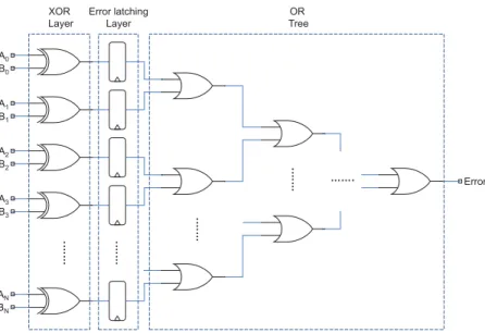
One solution to this problem is to move the error latching mechanism upstream in the OR-tree. This will not only reduce the difference in the lengths of paths a glitch or a delayed transition has to travel before reaching the FFs in the output register and the error latching mechanism but
2.1 Fault-Tolerance Techniques 23 … … . … … . ……. B0 A1 B1 A2 B2 A3 B3 AN BN Error A0 Error latching Layer XOR Layer 0 OR Tree … … . … … .
Fig. 2.3: An static comparator with Error Latching mechanism moved upstream
also blocks the unwanted signal perturbations from causing excessive power dissipation in the OR-tree. But even if the error latching mechanism is moved all the way up till the XOR gates as shown in Figure 2.3, the architecture will not meet the power consumption of the first scheme (of Figure 2.2a) because the XOR gates will still experience the unwanted activity and the increased number of FFs to latch error cause higher power consumption due to constant activity of clock network. Alternatively, a latching mechanism at the end of the OR-tree can be used with a delayed clock to latch the error. This clock offset should match the delay of the OR-tree to prevent any glitches from escaping detection. But due to process variations it is difficult to match and could not guarantee zero glitch escapes. On top of that the switching activity in the OR-tree will still be there.
To address some of the problems due to static comparator used in duplication with comparison, the work in [93] proposes a circuit-level implementation of a special comparator discussed in the following subsection.
Pseudo-dynamic Comparator: The main idea is to use an error latching mechanism upstream
in the OR-tree. Secondly, instead of depending on a capture edge to latch the error signal it uses a user defined comparison-window for detection of permanent, transient and timing errors. Furthermore it reduces the power consumption in the error latching layer by the use of DOR gates shown in Figure 2.4.
……. … … . ……. B0 A1 B1 A2 B2 A3 B3 AN BN Error A0 … … . ……. B0 A1 B1 A2 B2 A3 B3 A0 DC CompReset DOR DOR DOR XOR Layer 0 OR Tree BN-3 AN-2 BN-2 AN-1 BN-1 AN-3 Error latching Layer
Fig. 2.4: Pseudo-dynamic Comparator [93]
Figure 2.5 shows the structure of the 4-input DOR gate. The dynamic logic part, which is controlled by CompReset and DC signals forms an OR gate and the keeper acts as an error latching mechanism. During the pre-charge phase, reset is at logic-0. Input capacitance of the
inverteris pre-charged to VDD, which puts the Error signal at logic-0. During the evaluation phase
CompResetand DC are both at VDD. If atleast one of the inputs (Ci) turns to logic-1, the discharge
will occur. Consequently, Error switches to logic-1. Note that once the discharge happens, Error will remain at logic-1 until the next pre-charge phase. Besides, the keeper must be weak enough so that its input can be pulled down to logic-0 by the driving transistors.
Figure 2.6 present the complete error detection architecture using the pseudo-dynamic com-parator represented by the block labeled as ‘==?*’. It places the pseudo-dynamic comcom-parator across the output register in order to protect it against SEUs that are generated in it. The
Com-pResetand DC and the control logic that generates them is not show for clarity. Experimental
2.1 Fault-Tolerance Techniques 25 C0 C1 C2 C3 CompReset CompReset DC Error VDD GND Inverter Keeper VDD Dynamic Logic
Fig. 2.5: 4-input DOR gate [93]
In p u t R e g is te r O utput Regi s ter ==?* Error Input Output CL1 CL2
Fig. 2.6: Error detection architecture using the pseudo-dynamic comparator [93]
capability due to its error latching layer moved upstream in the OR-tree and with the use of dynamic logic it offers about 30% reduction in power compared with a static comparator, while having negligible area overhead in comparison with a static comparator.
2.1.1.2 Error Detecting Codes
Another widely used techniques of error detection in digital circuits is the use of error detecting codes. Error detecting codes introduce redundancy in information representation to detect possible errors in that representation [54]. Consider a logic circuit that performs a function f on the n-bit
input data i and produces a m-bit output f(i) as shown in Figure 2.7. Using error detecting
codes to improve the data integrity of this logic block generally involves implementing a block which predicts some special characteristic C(i) of the output f (i) for every input sequence i. A
checker circuit first computes this characteristic C′( f (i)) of output from the output itself and
logic function (f) Input (i) n Output Characteristic Predictor Output f(i) m Checker ==? Compaction k Error k Predicted characteristic C(i) Computed characteristic C’(f(i))
Fig. 2.7: General architecture of Error Detection with Codes [63]
Error detecting codes have been widely used to protect memories against SEUs and permanent faults [74]. The main reason of their widespread use in memories is that their regular structure allows efficient incorporation [28]. Use of error detecting codes to detect errors in logic circuit has been preliminarily based on the idea of reducing the implementation overhead of duplication with comparison. However reducing area overhead below the cost of duplication for random logic require redesigning the original circuits or compromising on fault coverage [38].
2.1.2
Error Recovery
Following an error detection an error recovery mechanism restores the error-free state of the system or prevents faults from being activated again or both [54]. Error recovery mechanism generally take two forms discussed in following subsections.
2.1.2.1 Rollback Error Recovery
In rollback recovery scheme errors are recovered by repeating the operation(s). Architectures based on rollback recovery generally use spatial redundancy to detect errors and correct them with temporal redundancy. Hardware and software use check-pointing to periodically or occasionally save system state, which is used to bring the system back to an error free state in case of error detection. These rollbacks can be as long as upto several thousands of cycles [62] or can be just one cycle deep [92].
An example of a single cycle deep rollback recovery scheme is shown in Figure 2.8a in which a concurrent error detection mechanism checks for errors at the end of each cycle and if it detects an error the instruction re-executes during the next cycle. Figure 2.8b shows an example of a much deeper rollback recovery scheme. After each computation, which takes several cycles an
![Fig. 1.1: Feature size and operating voltage scaling trend over years [22]](https://thumb-eu.123doks.com/thumbv2/123doknet/7716085.247959/27.892.123.787.166.417/fig-feature-size-operating-voltage-scaling-trend-years.webp)
![Fig. 1.3: Single Event Effect Mechanism [9]](https://thumb-eu.123doks.com/thumbv2/123doknet/7716085.247959/31.892.114.791.164.457/fig-single-event-effect-mechanism.webp)
![Fig. 2.4: Pseudo-dynamic Comparator [93]](https://thumb-eu.123doks.com/thumbv2/123doknet/7716085.247959/45.892.244.670.168.681/fig-pseudo-dynamic-comparator.webp)
![Fig. 2.7: General architecture of Error Detection with Codes [63]](https://thumb-eu.123doks.com/thumbv2/123doknet/7716085.247959/47.892.219.690.164.386/fig-general-architecture-error-detection-codes.webp)