HAL Id: hal-00379624
https://hal.archives-ouvertes.fr/hal-00379624
Submitted on 11 Apr 2020
HAL is a multi-disciplinary open access
archive for the deposit and dissemination of
sci-entific research documents, whether they are
pub-lished or not. The documents may come from
teaching and research institutions in France or
abroad, or from public or private research centers.
L’archive ouverte pluridisciplinaire HAL, est
destinée au dépôt et à la diffusion de documents
scientifiques de niveau recherche, publiés ou non,
émanant des établissements d’enseignement et de
recherche français ou étrangers, des laboratoires
publics ou privés.
Plasma doping implant depth profile calculation based
on ion energy distribution measurements
L. Godet, Z. Fang, S. Radovanov, S. Walther, E. Arevalo, F. Lallement, Jt
Scheuer, T. Miller, D. Lenoble, G. Cartry, et al.
To cite this version:
L. Godet, Z. Fang, S. Radovanov, S. Walther, E. Arevalo, et al.. Plasma doping implant depth profile
calculation based on ion energy distribution measurements. Journal of Vacuum Science & Technology
B Microelectronics and Nanometer Structures, American Vacuum Society (AVS), 2006, 24, pp.2391.
�10.1116/1.2353841�. �hal-00379624�
distribution measurements
*
L. Godet,a兲 Z. Fang, S. Radovanov, S. Walther, and E. Arevalo
Varian Semiconductor Equipment Associates, 35 Dory Road, GL-17 Gloucester, Massachusetts 01930
F. Lallement
STMicroelectronics, Crolles 38926, France
J. T. Scheuer and T. Miller
Varian Semiconductor Equipment Associates, 35 Dory Road, GL-17 Gloucester, Massachusetts 01930
D. Lenoble
STMicroelectronics, Crolles 38926, France
G. Cartry and C. Cardinaud
Institut des Matériaux Jean Rouxel, CNRS-Nantes University, Nantes 44322, France
共Received 16 February 2006; accepted 16 August 2006; published 25 September 2006兲
In traditional beamline implantation, the incident ion mass and energy are well known parameters and simulation programs are available to predict the implant profiles. In plasma based ion implantation, all ionized species present in the plasma are extracted and implanted by applying negative voltage pulses to the wafer. Therefore, prediction of implant profile is more complicated since it requires the knowledge of relative abundance of each ion species as well as their energy distribution prior to entering the wafer surface. This information is not readily available using conventional plasma characterization techniques because most of them measure plasma bulk properties. In order to collect the information needed for predicting plasma implant profiles, an ion mass and energy spectrometer is installed at the wafer level to allow in situ measurement of ion mass and energy distribution. In this paper, BF3plasma in the pressure range from 30 to 250 mTorr is studied. The relative flux and energy distribution of B+, BF+, BF
2
+, and BF 3
+ions striking the wafer
surface with energies up to 1 keV are measured. As expected, no energy contamination was observed during a plasma doping implantation and the maximum energy of the ions is defined by the cathode voltage. Based on the spectrometer data, a series of simulations was performed to calculate the boron and fluorine dopant depth profiles. The calculated profiles were in good agreement with secondary ion mass spectrometry 共SIMS兲 results and give some additional explanations of the unique surface-peaked SIMS profile of plasma doping implantation. © 2006 American Vacuum Society. 关DOI: 10.1116/1.2353841兴
I. INTRODUCTION
Transistor doping challenges at advanced technology nodes, as illustrated by the recent International Technology Roadmap for Semiconductors共ITRS兲, include high dose low energy implants for gate, source-drain, and source-drain ex-tension dopings.1,2 At low implant energies, traditional beamline technology suffers from low beam transport effi-ciency due to space charge related difficulties. A beamline implanter, running in decel mode, can achieve higher beam current. Unfortunately, ions can undergo charge exchange collisions with residual gas creating fast neutrals. Unaffected by the decel lens, these fast neutrals reach the wafer with a higher energy than desired. The beamline implanter applica-tions are limited by this energy contamination problem.3The use of a cluster beam is another approach to improve low energy performance, though its production worthiness has not been completely demonstrated.4
Plasma doping is a very promising candidate for source-drain extension doping for the technology node below 65 nm, as it can provide low-energy implantation and very high doses. It allows for less integration steps 共no offset spacers兲 and better or equal electrical performance as com-pared to traditional ion implantation.5 Plasma doping has been developed to meet the low energy high dose implant needs.5It has been demonstrated that plasma doping共PLAD兲 profiles are shallow, abrupt, and surface peaked over the en-ergy range of 0.05– 10 kV.6,7A PLAD implant profile is de-termined not only by the implant energy and dose, as in the beamline case, but also by parameters such as plasma density and composition. The principle and detailed description of PLAD can be found elsewhere,8and only a brief introduction is given here.
The glow discharge PLAD chamber consists of an anode and a cathode, which holds the wafer being implanted. A negative dc voltage pulse is applied to the cathode, which generates a glow discharge in the volume adjacent to the wafer. The plasma is ignited by each voltage pulse applied to the wafer, and at the pulse end, plasma follows a natural
*No proof corrections received from author prior to publication.
a兲
Author to whom correspondence should be addressed; electronic mail: [email protected]
decay process. During the pulse-on period, ions in the plasma are accelerated by the electric field across the plasma sheath and are subsequently implanted into the wafer. The energy of ions striking the wafer during pulse-on period is mainly controlled by the applied voltage. Other parameters such as pulse width, frequency, gas pressure, flow rate, sur-face condition, and geometry of electrodes can also affect the implant process by changing plasma composition, ion flux, and the number of collision inside the sheath. One parameter of particular interest to plasma doping is gas pressure. This parameter affects collisions between ions and neutrals in the sheath, which can alter the ion’s energy. In this paper, the gas pressure effect is examined in detail and its impact to dopant profile is fully characterized in the sub-kilovolt range.
We use the computer simulation package Stopping and Range of Ions in Matter9,10共SRIM兲 to predict dopant profiles
of all species and energies allowed by the PLAD voltage. The plasma implant profile is constructed from the individual profiles at different energies with their contributions propor-tional to the relative amount of ions at these energies. The essential information for profile calculation are the ion mass and energy distribution, which are measured in situ in the center of the wafer using an ion mass and energy spectrom-eter. Due to the pulsed plasma nature, the ion energy distri-bution of the ions striking the cathode changes over time during the plasma development and decay, therefore time resolved measurements are necessary. In this particular pa-per, the effect of the discharge pressure on the ion energy distribution (IED)of the ions striking the wafer during the pulse-on period is studied using the time resolved operation mode of the mass spectrometer.
II. EXPERIMENTS
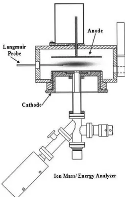
Figure 1 shows a schematic drawing of the PLAD cham-ber, where implants and plasma diagnostic experiments were carried out. The pulsed plasma is produced between two par-allel electrodes: a grounded anode and a negatively biased cathode on which the silicon wafer is loaded. An electro-static quadrupole probe (EQP)analyzer from Hiden Analyti-cal Inc. is installed below the wafer. A small aperture at the center of the wafer allows ions to enter the analyzer.
The Hiden EQP system consists of an electrostatic ion energy analyzer followed by a quadrupole mass spectrom-eter. It is electrically isolated from the cathode by a differen-tially pumped vacuum gap. A high vacuum level 共⬍5 ⫻10−8Torr兲 is maintained to eliminate any collisions inside the EQP system. The aperture size on the Si wafer is 100m, which is selected according to the chamber pressure and vacuum level required inside EQP. The use of a Si wafer with a small aperture also eliminates any metal contamina-tion risk inside the process chamber. Modificacontamina-tions to the extraction sector of the analyzer are made to achieve high ion transmission efficiency 共⬎95% 兲 over the energy range 共0 – 1000 eV兲.11
For time resolved measurements, the EQP analyzer is gated by a transistor-transistor logic 共TTL兲 pulse, 0 – 5 V, that is synchronized with the PLAD voltage pulse. A 2s
time resolution is achievable with the current EQP probe. The delay time between the TTL pulse and PLAD pulse is adjustable to allow ion sampling at the beginning, middle, and end of the PLAD pulse. The TTL pulse width is opti-mized taking into account the trade-off between good time resolution and low count rate. We measure ion energy from 0 to 1000 eV. In the steady state, the energy of each ion species is well known and the mass spectrometer time reso-lution is adequate. During the rise and fall times of the pulse, the time resolution is insufficient to accurately determine the shape of the IED. However, during these dynamic changes, the relative ion flux measured remains valid. In this paper, the steady state ion energy distributions are normalized to the relative total ion flux, defined as the sum of the ion energy distribution of all the ions reaching the cathode.
To collect PLAD dopant profiles, n-type prime Si 共100兲 wafers with 12 Å of control thermal oxide were implanted using PLAD with different plasma parameters. For this study, 0.5 kV and 1000 V PLAD pulses with 50s pulse-on time and 2.5 kHz frequency共12.5% duty cycle兲 were applied to the wafer. The BF3 pressure in the process chamber
ranged from 30 to 70 mTorr for 1 kV PLAD and from 75 to 250 mTorr for 0.5 kV PLAD. The as-implanted boron profile was analyzed using secondary ion mass spectrometry 共SIMS兲 with 700 eV O2+at 45° incidence angle with O
2leak.
As the coimplanted fluorine plays an important role during the activation of dopant,12 as-implanted fluorine profile was also collected using SIMS with 500 eV Cs+at 60° incidence angle without O2leak. The dose errors for all measurements
are expected to be less than 20%. The absolute error in the junction depth, Xj, should be less than 10%. This absolute
FIG. 1. Schematic diagram of PLAD process chamber with ion mass/energy analyzer and a Langmuir probe.
error is mainly due to discrepancies among techniques共e.g., nuclear reaction analysis, Rutherford backscattering spec-trometry, etc.兲 and laboratories which are used to calibrate the SIMS equipments.13 These conditions allow accurate measurement of profile shape, but less accurate measurement of total dose.
III. RESULTS AND DISCUSSION
In Fig. 2, we show the voltage and current wave forms measured during a 1 kV, 40 mTorr BF3discharge. The
cur-rent pulse has a sharp peak at the leading edge, which is mainly due to displacement current.14As soon as the voltage pulse is applied, a dynamic process starts in the discharge chamber where the neutrals and charged particles adjust their quantity, position, and energy until a steady state is reached. Characterization of the dynamic process is difficult.15A con-cern associated with pulse rise and fall times is that it may affect the ion mass and energy distribution, thus changing the implant profile. This concern was ruled out in early studies on low energy BF3PLAD implantation, as boron SIMS pro-files showed no difference for different pulse-on widths16 共20– 60s兲 with constant rise and decay times. The IEDs are changing during the rise and fall times of the pulse-on period. During these dynamic changes, the ion density and the ion energy are lower than during the flat part of the pulse. In Fig. 3, we report the time evolution of the different ion fluxes measured with the mass spectrometer during the PLAD pulse. During the first 10s of the pulse-on period, the sheath expands and the relative ion flux increases. After 15s, the relative total ion flux is stabilized and the IEDs of the different ions remain the same. During the decay, the total ion flux decreases as the sheath collapses. This obser-vation allows us to improve the statistics of the EQP system by employing a wide TTL gate pulse starting at 20s after the beginning of the pulse and ending at 50s. Therefore, only the constant portion of the pulse will be used to calcu-late the dopant depth profile. The rise and fall parts of the voltage pulse will not be included in the measurement and calculation as they do not contain any critical information for implant profile calculation.
In order to understand the shape of the energy distribution of different ion species reaching the cathode, a good under-standing of the sheath dynamics is necessary. In all the ex-periments reported here, the discharge is operated at rela-tively higher pressures where the collision mean free path 共兲 is short, so that many collisions occur within the sheath of thickness s. Unfortunately, certain approximation has to be used to describe the neutral interaction because ion-neutral cross sections for a BF3 discharge are not well
known. The hard sphere model is used here to estimate the ion-neutral cross section for a BF2+ion. In this paper, a con-stant ion-neutral cross section of 2 ⫻ 10−15cm2 will be as-sumed for different pressures and cathode voltages. The number of collisions共s / 兲 inside a sheath is calculated based on the collisional Child law17–19 by using the formula 共1兲. The assumptions are that the ion motion is highly collisional and charge exchange is the dominant ion-neutral collision mechanism; therefore the sheath thickness is significantly larger than the mean free path,
s =
冋
冉
2 3冊冉
5 3冊
3/2 0冉
2e M冊
1/2冉
kTg冊
2V 0 3/2p2 ji册
2/5 , 共1兲 where 0is the permittivity of free space, e is the charge ofan ion of mass M, is the ion-neutral cross section, k is Boltzmann’s constant, Tg is the gas temperature, V0 is the
cathode voltage, p is the neutral-gas pressure, and ji is the
ion current density. The ion current density is calculated us-ing the followus-ing formula:
ji=
Ic
ac共1 +␥兲
, 共2兲
where Icis the measured cathode current, acis the cathode
area, and ␥ is the secondary electron emission coefficient which was experimentally determined for our apparatus.20In these experiments, the secondary emission current is a sig-nificant fraction of the measured cathode current and is taken into account during the calculation.
In Fig. 4, we show the number of collisions inside the sheath calculated with relation共1兲 for different gas pressures
FIG. 2. Cathode voltage and current wave forms for a 1 kV, 40 mTorr, 50s, 2.5 kHz BF3discharge.
FIG. 3. Evolution during the pulse of the relative total ion flux and B+, BF+,
and two extreme cathode voltages, 500 and 1000 V 共dis-charge cannot be ignited below 500 V, and due to the limi-tation of the mass spectrometer to ion energy below 1000 eV, 1000 V corresponds to the maximum energy that we can measure兲. When the cathode bias voltage is at 1 kV, the discharge pressure is limited by the Paschen curve to a range from 30 to 70 mTorr. For this pressure range the num-ber of collisions inside the sheath remains constant 共s / re-mains constant兲. The decrease of the mean free path at higher pressure is compensated by the decrease of the sheath thick-ness due to plasma density increase at higher pressure. Con-sequently, minor changes in the shape of the IED are ex-pected. When a lower bias voltage is used 共0.5 kV兲, the discharge can be operated under a large range of pressures from 75 to 250 mTorr. Within this pressure range, the num-ber of collision increases from 6.9 to 10.3, thus causing sig-nificant changes in the IED. This is in agreement with our experimental observations.
In Fig. 5 we show the cathode current for different
rela-tive ion fluxes for the 1 kV bias voltage. The cathode current is increasing rapidly from 75 mA at 30 mTorr to 375 mA at 70 mTorr. At the same time the total relative ion flux in-creases from 5.2⫻ 107 to 2.6⫻ 108 in unit of counts/s. A
linear relationship is observed between cathode current and relative total ion flux. In the case of the 0.5 kV BF3 dis-charge, the linear relationship is still valid over the large range of pressures. As the secondary emission yield 共␥兲 is almost constant with pressure, the cathode current is propor-tional to the ion current关relation 共2兲兴 and thus to the ion flux 共ion flux is equal to ion current times elementary charge兲. The linear relation between ion flux measured by the mass spectrometer and the cathode current suggests a constant transmission inside the mass spectrometer in this pressure range.
The ion mass and energy distribution of a 1 kV BF3
plasma at three different pressures is presented in Fig. 6. As discussed previously, the pressure changes do not affect sig-nificantly the shape of the IED except for the BF3+ion. In all cases, BF3+fraction remains very low共less than 2%兲. BF3+has
a smaller energy spread and the peak of the IED is in a thermal range. BF2+is the most abundant ion implanted into the wafer with more than 60% of the total boron ion flux composed of B+, BF+, BF2+, and BF3+. Only a few ions 共⬍1 % 兲 from the boron ion flux are able to reach the wafer with full energy 共1000 eV兲. The majority of the ions strike the cathode with energy lower than 500 eV. Due to the col-lisions inside the sheath, typical ion energy distributions have a large energy spread producing shallow and more abrupt as-implanted SIMS profile than an equivalent 1000 eV beamline implant, where all the ions strike the wa-fer with the full energy.
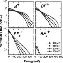
The normalized IED of 0.5 kV BF3 discharge in a range
of pressure共100– 250 mTorr兲 is shown in Fig. 7. The maxi-mum energy of B+, BF+, and BF2+ is reduced significantly when the pressure is raised from 100 to 250 mTorr. Com-pared to the 1 kV case, the number of collision inside the sheath is significantly increased. Only few ions 共⬍0.1% 兲 from the boron ion flux are able to reach the wafer with full
FIG. 4. Ratio of sheath thickness over ion mean free path s / as a function of the pressure for different cathode voltage共1 kV and 500 V兲. s / is an estimation of the number of collisions for an ion crossing the high voltage sheath in front of the cathode.
FIG. 5. Cathode current vs relative total ion flux measured with the mass
spectrometer for 1 kV 共30– 70 mTorr兲 and 500 V 共75– 250 mTorr兲 BF3
plasma.
FIG. 6. B+, BF+, BF2+, and BF3+IED normalized to the total ion flux for 1 kV
BF3plasma at three different pressures: 30, 50, and 70 mTorr.
energy共500 eV兲. The majority of these ions 共91%兲 strike the cathode with energy lower than 250 eV. The ion energy and the lighter ion fraction slightly decrease with the pressure, which should provide shallower dopant depth profile as con-firmed by previous experiments.16Figure 8 shows that BF2+is the dominant ion reaching the cathode for all the different process conditions and the fraction of BF3+is lower than 1% of total ion flux. The increase of collisions inside the sheath does not significantly affect the ratio between the different ions.
IV. CALCULATION OF THE PREDICTED DOPANT DEPTH PROFILE
The measured IED for all the boron and fluorine ions implanted into the wafer was used as an input into an implant simulation software. TheSRIMwas used to simulate and pre-dict an implant profile and the results were compared to the profiles measured by SIMS.21 Since SRIM only accepts atomic ions, the BFx+ 共x = 1 , 2 , 3兲 IEDs are converted into
equivalent boron IED Beq+ and equivalent fluorine IEDs Feq+ by using the following formulas:
E共Beq+兲 = E共BFx +兲 mB mBFx+ , 共3兲 E共Feq+兲 = E共BFx +兲 mF mBF x +. 共4兲
Figure 9共a兲 shows the equivalent boron and fluorine IEDs under the previous discharge conditions. As expected, the majority of the boron and fluorine equivalent ion energies are below 250 eV. Less energetic equivalent boron is obtained for higher pressure, but the low energy tail is not signifi-cantly affected关Fig. 9共b兲兴. The equivalent boron and fluorine energies are partitioned into energy bins with 10 eV incre-ments. Each energy bin defines an ion dose fraction of the total ion flux coming onto the wafer. The average energy of each bin is used as the input energy for theSRIMsimulation. Then all the output depth profiles fromSRIMare added up to represent the predicted depth profile based on the IED of all the ions striking the wafer. The predicted boron and fluorine profiles are compared to the experimental boron and fluorine
FIG. 7. B+, BF+, BF 2 +, and BF
3
+IED normalized to the total ion flux for
500 kV BF3 plasma at four different pressures: 100, 150, 200, and
250 mTorr.
FIG. 8. Ion ratio in a 500 V BF3 plasma with pressure ranging from
75 to 225 mTorr.
FIG. 9. 共a兲 Boron and fluorine equivalent energies based on the 500 V, 100 mTorr IED of the ions reaching the wafer.共b兲 Boron equivalent energy based on the 500 V IED of the ions reaching the wafer for a large range of pressure共75– 250 mTorr兲.
SIMS profiles on Fig. 10共a兲. A good agreement is obtained between the simulation and the experimental SIMS profiles for both elements. On the boron and fluorine SIMS profiles, we clearly see the typical channeling tail22inside the crystal-line wafer. This was not reflected in the predicted profiles becauseSRIMsimulation assumes an amorphous target. This
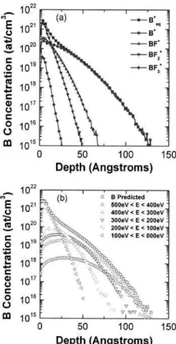
channeling tail, obtained at 0.5 and 1 kV with a crystalline silicon wafer, confirmed that the ions reach the wafer with a small angle. When a preamorphized implanted 共PAI兲 sub-strate is used, no channeling tail is observed and the pre-dicted boron profile matches also the deeper part of the mea-sured SIMS profile for the 0.5 kV case关see “B SIMS PAI” curve on Fig. 10共a兲兴. As expected, based on the boron equivalent energy distribution, shallower boron profiles are obtained when the pressure increases from 100 to 250 mTorr 关see Fig. 10共b兲兴. No difference on the boron SIMS profile was observed when the pressure was raised from 30 to 70 mTorr as expected with the 1 kV mass spectrom-eter data and the predicted profiles shown in Fig. 10共c兲. By doing the simulation for each ion separately for the 0.5 kV, 100 mTorr PLAD, the particularities of a PLAD dopant pro-file共surface peak and very shallow profile兲 can be explained. Figure 11共a兲 shows the role of each ion species reaching the wafer; B+defines the depth of the implant, BF+and BF
2 +are
the main contributors to the surface dose, and BF3+does not have significant impact on the SIMS profile. Thus, in order to meet the junction depth requirements of the ITRS for tech-nological nodes below 65 nm, the B+ion flux fraction needs to be minimized by controlling the plasma parameters共bulk plasma optimization兲 and the collision processes inside the
FIG. 10. 共a兲 Boron and fluorine predicted depth profiles based on the mea-sured ion mass and energy distribution for crystalline and preamorphized silicon wafer共PAI兲, compared with the measured SIMS depth profile for the same implant conditions 共500 V, 100 mTorr BF3PLAD兲. 共b兲 Boron
pre-dicted profile of 500 V BF3PLAD at 100, 150, 200, and 250 mTorr.共c兲
Boron predicted depth profile based on the measured ion mass and energy distribution, compared with the measured SIMS depth profile for the same implant conditions共1 kV, 30– 70 mTorr BF3PLAD兲.
FIG. 11.共a兲 Contribution of each ion reaching the wafer 共B+, BF+, BF 2 +, and
BF3+兲 onto the boron depth profile. 共b兲 Contribution of each energy bin
共0 – 100 eV, 100– 200 eV, 200– 300 eV, 300– 400 eV, and 400– 500 eV兲 equivalent boron energy onto the boron depth profile.
cathode sheath. This subject will be discussed in another paper 共see also Ref. 11兲. It is also found that ions with equivalent energy between 0 and 100 eV are the main con-tributors to the dose and the surface peak of a PLAD SIMS profile which represents about 50% of the total dose 关Fig. 11共b兲兴. The higher energy ions are found to define the final dopant depth. Therefore, another approach to reduce the junction depth could be to increase further the number of collision and reduce the B+mean energy rather than trying to reduce the B+fraction.
V. SUMMARY AND CONCLUSION
In situ mass and ion energy distribution data were col-lected with an ion mass and energy spectrometer installed in the middle of the cathode. These data were used to predict the plasma implant profiles of a BF3 plasma based ion im-plantation. Plasma in the pressure range from 30 to 250 mTorr, as well as the relative flux and energy dis-tribution of B+, BF+, BF
2
+, and BF 3
+ ions striking the wafer
surface with energies up to 1 kV, was studied in this paper. Based on the spectrometer data, a series ofSRIMsimulations was performed to calculate the boron and fluorine dopant depth profiles. The calculated profiles match the ones mea-sured by secondary ion mass spectrometry共SIMS兲 and give some additional explanations of the surface-peaked SIMS profile unique to plasma doping. Such knowledge will be useful in controlling and optimizing implant profiles and dopant activation.
1
International Technology Roadmap for Semiconductors→ Front End Pro-cesses, Semiconductor Industry Association, p. 23, 2005, http:// www.itrs.net/Common/2005ITRS/FEP2005.pdf
2John O. Borland, Tomoko Matsuda, and Keiji Sakamoto, Solid State
Technology, pp. 83–94, June 2002
3A. Renau and J. T. Scheuer, Proceedings of the 14th International
Con-ference on Ion Implantation Technology, Taos, September 2002 共unpub-lished兲, p. 151.
4Z. Fang, E. Arevalo, Tim Miller, Harold Persing, Edmond Winter, and V.
Singh, Proceedings of IWJT 2004共unpublished兲.
5F. Lallement et al., Symp. VLSI Tech. Dig. 2004, 178. 6J. T. Scheuer et al., Surf. Coat. Technol. 186, 57
共2004兲.
7S. B. Felch, D. Lenoble, A. Grouillet, E. Arevalo, S. R. Walther, Z. Fang,
B.-W. Koo, and R. B. Liebert, Proceedings of the 13th International Con-ference on Ion Implantation Technology, Alpbach, Austria, September 2000共unpublished兲.
8B.-W. Koo, Z. Fang, L. Godet, S. Radovanov, C. Cardinaud, G. Cartry, A.
Grouillet, and D. Lenoble, IEEE Trans. Plasma Sci. 32共2004兲.
9Stopping and Range of Ions in Matter
共SRIM兲, a numerical simulation by J. F. Ziegler and J. P. Biersack, http://www.srim.org/
10J. F. Ziegler, Ion Implantation: Science and Technology, edited by J. F.
Ziegler共Ion Implantation Technology, Edgewater, MD, 1996兲.
11Ludovic Godet, Ph.D. thesis, Nantes University, 2006.
12E. Ishida, D. F. Downey, K. S. Jones, and J. Lui, Proceedings of the 1998
International Conference on Ion Implantation Technology共IEEE, New York, 1999兲, Vol. 2, pp. 909–912.
13T. H. Buyuklimanli, C. W. Magee, and J. W. Marino, J. Vac. Sci. Technol.
B 24, 408共2006兲.
14Z. Fang, Bon-Woong Koo, Susan Felch, Yu Lei, Lawrence J. Overzet, and
Matthew Goeckner, Proceedings of the 14th International Conference on Ion Implantation Technology, Taos, September 2002 共unpublished兲, p. 403.
15S. Radovanov et al., J. Appl. Phys. 98, 113307共2005兲. 16D. Lenoble, Ph.D. thesis, Toulouse University, 2000. 17M. A. Lieberman, J. Appl. Phys. 86, 2926共1989兲. 18R. A. Stewart and M. Lieberman, J. Appl. Phys. 70, 3491
共1991兲.
19Casper V. Budtz-Jorgensen, Ph.D. thesis, Faculty of Science, Aarhus
University, 2001.
20Timothy Miller共unpublished兲.
21Steve Walther, Ludovic Godet, T. Buyuklimanli, and J. Weeman, J. Vac.
Sci. Technol. B 24, 489共2006兲.
22Steve Walther and Reuel Liebert, J. Vac. Sci. Technol. B 24, 482