UNIVERSITÉ DE MONTRÉAL
ORGANIC GATE DIELECTRICS FOR TETRACENE
FIELD EFFECT TRANSISTORS
SIMONE BERTOLAZZI
DÉPARTEMENT DE GÉNIE PHYSIQUE ÉCOLE POLYTECHNIQUE DE MONTRÉAL
MÉMOIRE PRÉSENTÉ EN VUE DE L’OBTENTION DU DIPLÔME DE MAÎTRISE ÈS SCIENCES APPLIQUÉE
(GÉNIE PHYSIQUE) DÉCEMBRE 2010
UNIVERSITÉ DE MONTRÉAL
ÉCOLE POLYTECHNIQUE DE MONTRÉAL
Ce mémoire intitulé:
ORGANIC GATE DIELECTRICS FOR TETRACENE
FIELD EFFECT TRANSISTORS
présenté par : BERTOLAZZI Simone
en vue de l’obtention du diplôme de : Maîtrise ès sciences appliquée a été dûment accepté par le jury d’examen constitué de:
M. MASUT Remo A., Ph.D., président
Mme SANTATO Clara, Ph.D., membre et directrice de recherche M. ROSEI Federico, Ph.D., membre et codirecteur de recherche M. DESJARDINS Patrick, Ph.D., membre.
DÉDICACE
A mio padre e mia madre
« Si tu veux construire un bateau, ne rassemble pas des hommes pour aller chercher du bois, préparer des outils, répartir les tâches, alléger le travail… mais enseigne aux gens la nostalgie de l’infini de la mer »
ACKNOWLEDGMENTS
There are many people that I want to thank, without whom this work would not have been possible. First of all, I want to express my gratitude to my supervisor, Clara Santato, for introducing me to organic electronics and to the world of scientific research. I owe her much in terms of scientific knowledge and methods: she taught me how to tackle a scientific problem and let me participate in high-level scientific activities, including the MRS conference in Boston, F-Pi-9 in Atlanta and the research experience at the synchrotron in Trieste, Italy.
I thank FQRNT (Fonds Québécois de la Recherche sur la Nature et les Technologies) for financial support and Politecnico di Milano for choosing me to participate in its double degree program at École Polytechnique de Montréal. It has been a unique experience and I am sure that I received a lot from many points of views; not only scientific knowledge and technical experience but also culture and humanity.
I want to thank all the laboratory technicians, for their silent but invaluable work, in particular Joël Bouchard and François Rigano. I am also thankful to Fabio Cicoira, Khalid Laaziri, Jacqueline Sanchez and Patricia Moraille for their precious technical and scientific advices. Here in Montréal I was surrounded by friendly people that supported me throughout this time. I am deeply grateful all the students in Clara Santato’s group for their friendship and for the good time spent together in the laboratory. I want also to thank Charles Brosseau and Gaëlle Terrom, who helped me to prepare the polymer dielectric layers and to carry out the AFM imaging of the tetracene films, and François La Pointe, for helping me with the silanization process.
Last but not least, a huge thanks to my family, who made the sacrifice to let me live abroad for more than two years, and to all the friends in Italy, in Canada and worldwide for helping me to take the right steps throughout my life.
RÉSUMÉ
Dans les trois dernières décennies, les couches minces de semiconducteurs organiques ont fait l’objet de recherches intensives. Ces couches peuvent être utilisées dans une grande variété de dispositifs optoélectroniques de nouvelle génération, tels que les diodes électroluminescentes (OLED), les transistors à effet de champ (OFET), et les cellules photovoltaïques. Récemment, des couches minces poly-cristallines de tétracène, sublimées sous vide, ont été utilisées pour réaliser le premier transistor organique à effet de champ émetteur de lumière (OLEFET), qui intègre dans un seul dispositif la fonction de modulation du courant typique d’un transistor avec la capacité de production de lumière d’une diode électroluminescente.
La démonstration des OLEFETs n’est pas simple. Tout d’abord, une intégration efficace des fonctions optiques et électroniques nécessite l’utilisation d’un semiconducteur électroluminescent ayant aussi des propriétés de transport de charge intéressantes. Deuxièmement, un transport de charge ambipolaire (i.e. de trous et d’électrons) doit être réalisé pour produire des OLEFETs à haute performance. Dans ce contexte, le contrôle de la chimie de surface du substrat diélectrique s’est révélé être une stratégie efficace pour limiter la suppression du transport des électrons induite par les états électroniques pièges à l'interface diélectrique/semiconducteur. En même temps, la modification de la nature chimique et physique du substrat diélectrique influence la morphologie/structure des couches minces organiques, qui à son tour influence la performance du dispositif.
Dans le cadre de ce projet, des couches minces poly-cristallines de tétracène – pour applications dans les OLEFETs – ont été sublimées sous vide sur différents substrats organiques diélectriques, y compris des polymères (parylène C, poly méthacrylate de méthyle, polystyrène) et des monocouches auto-assemblées d’hexaméthyldisilazane (HMDS) et octadécyltrichlorosilane (OTS). Le taux de dépôt était de 3.5 Å/s, la pression à l'intérieur de la chambre à vide était de 2.5×10⁻⁶ Torr, les substrats ont été maintenus à température ambiante.
Le processus de germination et croissance a été étudié à partir des premières étapes de la croissance jusqu’au recouvrement complet de la surface, au moyen de la microscopie à force atomique (AFM) ex-situ. La densité de nucléation, la forme des grains cristallins et leur
connectivité dépendent fortement des propriétés physiques et chimiques de la surface diélectrique.
Des transistors organiques à effet de champ, dans la configuration « bottom gate – top contact », ont été fabriqués pour explorer les propriétés de transport de porteurs de charge et l’électroluminescence des couches minces de tétracène déposées sur les différents substrats diélectriques organiques. L’utilisation des couches diélectriques organiques conduit à des valeurs de mobilité des porteurs de charge sensiblement différentes, variant entre 1∙10-2 et 2∙10-1 , la valeur la plus élevée étant celle des couches déposées sur du polystyrène.
Le prolongement naturel de ce travail est d'établir une corrélation entre le transport de charge, l'émission de lumière et la morphologie/structure des couches organiques pour applications dans les OLEFETs.
ABSTRACT
Over the last three decades, thin films of organic semiconductors (OS) have been the object of intense research. These films can be used in a wide variety of new-generation optoelectronic devices, such as Organic Light Emitting Diodes (OLED), Organic Field Effect Transistors (OFET) and photovoltaic cells. Recently, vacuum sublimed tetracene films were used to realize the first Organic Light Emitting Field Effect Transistor (OLEFET), which integrates in a single device the current modulation function of a FET with the light generation capability of a LED. The demonstration of OLEFETs is not straightforward. First of all, an efficient integration of optical and electronic functionalities requires the use of a semiconductor with both efficient electroluminescence and good charge transport properties. Secondly, an ambipolar charge transport has to be achieved to produce high performance OLEFETs. Within this context, controlling the dielectric substrate surface chemistry has proven to be an efficient strategy, since it contributes to avoid the suppression of the electron transport induced by the electronic trap states at the dielectric/semiconductor interface. At the same time, the modification of the chemical and physical nature of the dielectric substrate influences the morphology/structure of the organic thin-films, in turn influencing the final device performance.
In this work, polycrystalline tetracene thin films – to be incorporated in OLEFETs – were vacuum sublimed on different organic dielectric substrates, including polymers (parylene C, polymethylmethacrylate, polystyrene) and self-assembled monolayers of hexamethyldisilazane (HMDS) and octadecyltrichlorosilane (OTS). The scope of the work was indeed to shed light on the role of the organic dielectric surface in influencing the charge transport properties of tetracene OLEFETs.
The tetracene deposition rate was 3.5 Å/s, the substrates were kept at room temperature and the pressure inside the vacuum chamber was 2.5×10⁻⁶ Torr.
The growth process was studied from sub-monolayer to complete coverage by means of ex-situ Atomic Force Microscopy (AFM). The nucleation density, the grain size and the connectivity between the grains were observed to be strongly dependent on the physical and chemical properties of the dielectric substrate surface.
Thin-film transistors, in the bottom gate – top contact configuration, were fabricated to explore charge transport and electroluminescence in tetracene films vacuum sublimed on the different organic gate dielectrics. It was found that the use of the organic dielectric layers leads to considerably different values of the charge carrier mobility, ranging between 1∙10-2 and 2∙10-1 , the highest mobility being observed in the case of polystyrene.
The natural extension of this project is to establish a sound correlation between charge transport, light emission and film morphology/structure in organic thin films for applications in OLEFETs.
CONDENSÉ EN FRANÇAIS
Depuis les années 80, suite à la découverte des propriétés conductrices et semi-conductrices des polymères et des molécules organiques, s’est progressivement développée une nouvelle branche de l'électronique moderne, c’est-à-dire l’« électronique organique ».
L’intérêt pour l'électronique organique est motivée par les avantageuses propriétés de semi-conducteurs organiques, y compris un faible coût, la flexibilité mécanique, les basses températures de processus et la possibilité de les appliquer sur des substrats à large surface flexibles et enroulables. En outre, les propriétés optiques et électroniques de ces matériaux (par exemple le « gap » d’énergie entre la bande de conduction et la bande de valence) peuvent être facilement modifiés par des procédés de synthèse chimique et sont donc facilement adaptable aux besoins spécifiques des différentes applications.
L’utilisation de matières organiques à la place des semi-conducteurs inorganiques typiquement utilisés dans l'industrie microélectronique (par exemple, Si, Ge, GaAs), permet de fabriquer une grande variété de dispositifs optiques et électroniques parmi de processus de dépôt simples et peu coûteux, tels que le dépôt par solution (méthode de la tournette et dépôt par immersion) ou encore parmi une imprimante à jet d'encre. En plus, la flexibilité mécanique et les basses températures de traitement des matériaux moléculaires permettent de fabriquer des circuits électronique et optoélectronique sur des substrats de plastique flexible, enroulable et avec une très élevé extension superficielle.
Outre les produits tels que diodes (OLEDs) et transistors organiques à effet de champ (OFETs), déjà disponibles sur le marché, beaucoup d’autres applications sont à l’étude, comment par exemple des cellules photovoltaïques, des lasers ou des capteurs. Récemment, en 2003, un nouveau type de dispositif a été développé, à savoir le transistor organique à effet de champ émetteur de lumière (OLEFET), qui intègre dans une seule unité la fonction de modulation du courant typique d’un transistor avec la capacité de production de lumière d’une diode électroluminescente. L’OLEFET est intéressant d’un point de vue soit fondamental soit appliqué. Contrairement à l'OLED, qui è caractérise par une géométrie à empilement vertical, l’OLEFET est caractérise par un géométrie plane; ça permet l’accès direct à la surface des couches
organiques parmi des détecteurs optiques, ce qui rend possible l'étude des phénomènes physiques fondamentaux dans les matériaux semi-conducteurs organiques, tels que le transport de charge et l’électroluminescence.
Le premier prototype d’OLEFET utilisait comme matériau active des couches minces poly-cristallines de tétracène, qui font aussi l’objet de ce travail de maîtrise. Le premier OLEFET était caractérisé par un transport de charge unipolaire de type « p », où seulement des charges positives (trous) sont impliqués dans le phénomène de conduction de courant. Par conséquent, la région d’émission de la lumière était localisé à proximité de l’électrode d’injection des porteurs minoritaires (drain) et ça limitait l'efficacité du dispositif, en réduisant la formation et la recombinaison des excitons par un effet de « quenching » induit par le métal de l’électrode (Or). L’objectif général de ce travail était de donner une réponse à la question si est possible obtenir un transport de charge ambipolaire, c’est-à-dire un transport simultané des électrons et des trous, dans les transistors organiques à effet de champ basés sur des couches minces poly-cristallines de tétracène. L’approche adoptée a été l’ingénierie de la surface diélectrique. L’utilisation des diélectriques organiques, tels que des polymères ou des monocouches moléculaires auto-assemblées, a été démontré être une approche efficace pour obtenir un transport de charge ambipolaire. En fait, le contrôle de la chimie de la surface diélectrique permet de limiter la densité des états électroniques pièges présents à l’interface diélectrique- semiconducteur, qui sont responsable de la suppression du transport des électrons.
L’ambipolarité du dispositif est une propriété fondamentale pour les OLEFETs car permet de déplacer la position de la région de formation/recombinaison des excitons dans le canal du transistor, loin des électrodes, et en conséquence permet d’augmenter l’efficacité d’émission de lumière.
En 2007, Takahashi et al. ont démontré la possibilité de réaliser des transistors à effet de champ ambipolaires en utilisant des monocristaux de tétracène laminés sur des couches diélectriques de poly méthacrylate de méthyle (PMMA) et contactés par des électrodes avec une basse fonction de travail, tels que argent et magnésium; après cette découverte, la recherche de l’ambipolarité dans les couches minces poly-cristallines de tétracène est devenue significative et scientifiquement intéressant.
Pour différentes raisons, qui seront expliqué par la suite, nous n’avons pas pu observer le transport de type « n » (électrons) et cet étude à été focalisé principalement sur les propriétés morphologiques et structurelles des couches minces poly-cristallines de tétracène en corrélation avec la performance des correspondantes transistors organiques.
Les semiconducteurs organiques sont fortement sensibles à l’oxygène et à l’eau présents dans l’atmosphère ambiante, qui peuvent être adsorbé dans le dispositif – s’il n’est pas convenablement encapsulé – et induire la dégradation de leur performance. Per conséquent, a fin d’observer l’ambipolarité, un contrôle rigoureux de l'atmosphère pendant toutes les étapes de la fabrication et caractérisation des dispositifs est obligatoire. En plus, il est nécessaire d’optimiser l’architecture du dispositif, y compris le choix des matériaux pour les électrodes de « source » et « drain ». Ces dernières doivent être choisis attentivement, avec une faible fonction de travail, afin d’empêcher la formation de barrières d’injection pour les électrons entre l’électrode de « drain » et le canal semiconducteur du transistor.
Tous les aspects abordés (surface du substrat diélectrique, influence de l’eau e de l’oxygène, fonction de travail des électrodes métalliques) sont à la fois crucials pour l’observation d’un transport ambipolaire dans les couche minces de tétracène. Présentement, dans nos laboratoires, des difficultés expérimental doivent encore être résolues, comment le (i) développement d’un méthode pour la réalisation/caractérisation complète des dispositifs sous atmosphère inerte et (ii) la réalisation de dispositifs avec des électrodes de « source » et « drain » fabriqués en utilisant de matériaux différents, tels que Au-Mg (ou Au-Ca) respectivement. Seulement après que tous les aspects seront dûment pris en compte, on sera en mesure de donner une réponse claire sur le rôle que l’ingénierie de surface diélectrique joue sur le propriétés de transport de charge et donc on pourra répondre à la question concernant l’ambipolarité.
Le Chapitre 1 décrit les principes et l’architecture des OFETs et des OLEFETs (section 1.3 et 1.4) et présente plus en détail le but de cette travail de recherche (section 1.5).
Dans ce travail de maîtrise on à étudié les effets de la modification des propriétés chimiques et physiques de la surface diélectrique sur la morphologie/structure de couches minces et leurs effets sur la performance des transistors à effet de champ.
Des couches minces poly-cristallines de tétracène ont été sublimées sous vide sur différents substrats diélectriques organiques, y compris des polymères, tels que parylène C, poly méthacrylate de méthyle (PMMA) et polystyrène (PS), et des monocouches moléculaires auto-assemblées d’hexaméthyldisilazane (HMDS) et octadécyltrichlorosilane (OTS).
L’utilisation de diélectriques organiques influence le processus de croissance, la morphologie et la structure cristalline des couches poly-cristallines et par conséquence aussi leurs propriétés fonctionnelles. Le processus de germination et croissance a été étudié à partir des premières étapes de la croissance jusqu’au recouvrement complet de la surface, au moyen de la microscopie à force atomique (AFM) ex-situ.
L’objectif spécifique de cette étude était d’établir une corrélation entre les propriétés de la surface diélectrique (par exemple l’énergie de surface, la rugosité et la permittivité diélectrique) et le transport de charge. On a également entrepris une étude pour identifier une corrélation entre le mode de croissance, la morphologie des couches minces et la mobilité des porteurs de charge (trous). Pour faire cela, des dispositifs OFETs ont été fabriquées dans la géométrie « bottom gate – top contacts », où les électrodes d’Or ont été déposés directement sur la surface des couches de tétracène en utilisant une technique d’évaporation thermique et des « shadow masks ».
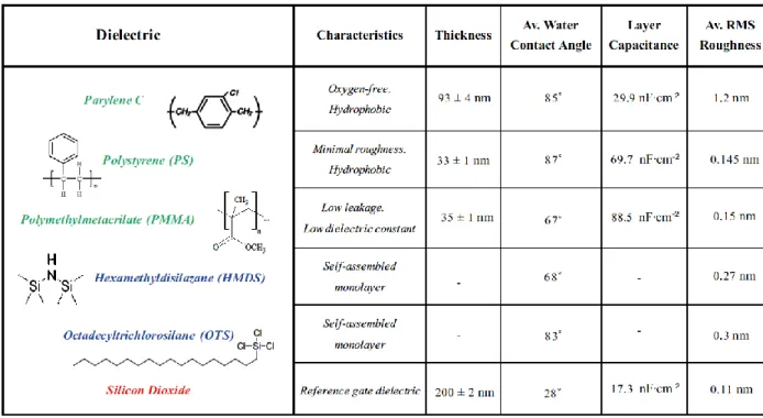
Le Chapitre 2 décrit les procédures et les techniques expérimentales utilisées pour le dépôt et la caractérisation soit des couches minces de tétracène soit des couches diélectriques organiques (polymères et monocouches moléculaires auto-assemblées). La mesure d’épaisseur des couches de polymères diélectriques a été effectuée par ellipsométrie spectroscopique et profilométrie. La méthode de l’angle de contact a été utilisée pour étudier la nature hydrophobe/hydrophile de la surface diélectrique et pour estimer l’énergie libre de surface.
La technique expérimentale plus largement utilisé a été la microscopie à force le atomique (AFM) avec laquelle il a été possible d’obtenir une pluralité d’informations sur la morphologie des substrats diélectriques et des couches minces de tétracène. Des mesures de diffraction de rayons X ont été aussi conduites au Synchrotron (ELETTRA, Trieste), en utilisant la technique appelée « Grazing Incidence X-Ray Diffraction » qui permette de caractériser la structure et la
texture de couches minces organique à l’interface entre le diélectrique et le semiconducteur. Le résultats sont actuellement en cours d’élaboration.
Dans le Chapitre 2 on décrit également la procédure adoptée pour la fabrication de dispositifs OFETs et OLEFETs et leur caractérisation électrique. Le point de départ a été un substrat de silicium hautement dopé (résistivité d’environ 0.001-0.005 Ohm∙cm) et oxydé thermiquement (épaisseur de l’oxyde de 200 nm), qui peut être convenablement utilisé soit comment substrat soit comment électrode de grille. Les couches diélectriques organiques ont été déposés sur la surface de l’oxyde en utilisant différentes techniques, y compris la méthode de la tournette (PMMA, PS et HMDS), la silanization par phase vapeur (OTS) et la polymérisation par dépôt chimique en phase vapeur (Parylène C).
Les couches minces de tétracène (épaisseur d’environ 50 nm) ont été sublimé sous vide sur le différents substrats diélectriques avec un taux de déposition de 3.5 Å/s. Les substrats ont été maintenus à la température de la pièce et la pression à l’intérieur de la chambre à vide était de 2.5 × 10⁻⁶ Torr. En suite, les électrodes d’or ont été évaporés thermiquement (épaisseur de 50 nm et un taux de dépôt de 1 Å/s) sur les couches organiques avec différents géométries (interdigités et à canal unique) et longueurs de canal. Le désavantage principal de cet approche est la petite résolution de la « shadow mask », qui ne permet pas de fabriquer de transistors avec une longueur de canal plus petite que 50 µm.
Le Chapitre 3 est dédié à la présentation et à la discussion des résultats expérimentaux. La première partie du chapitre (section 3.1) présente les résultats de l’étude de germination et croissance et les propriétés morphologiques des couches de tétracène déposées sur les différentes surfaces diélectriques. On a déposé des couches avec différents épaisseurs nominales (2, 5, 10, 17, 35 et 50 nm) qui en suite on été caractérisée par la microscopie à force atomique (AFM). On a identifié trois phases distinctes: (i) le début de la croissance (germination), (ii) le développement et la coalescence des îles, (iii) le recouvrement complet de la surface. La première observation à été le fait que la densité de nucléation, la forme des grains cristallins et leur inter-connectivité dépendent fortement des propriétés physiques et chimiques de la surface diélectrique.
La deuxième partie du chapitre (section 3.2) présente les résultats de caractérisation électrique des OFETs et montre les courbes de « output » et de « transfer » des dispositifs à canal unique fabriqués sur tous le différents substrats diélectriques.
On a réussi à fabriquer des transistor de tétracène de type « p », en employant tous cinq les couches diélectriques organiques (PMMA, PS, Parylene C, OTS, PMMA) et on rapporte les principaux facteurs de mérite, y compris la mobilité des porteurs de charge (trous), la tension de seuil et le rapport entre le courant de ON et le courant de OFF .
La mobilité des trous dépende significativement des propriétés de la surface diélectriques et varie dans une plage de valeurs plus large qu’un ordre de grandeur, entre 1∙10-2 cm2V-1s-1 (sur SiO2 non traité) et 2∙10-1
cm2V-1s-1 (sur PS). La valeur de mobilité obtenue dans le cas des couches minces des tétracène déposé sur PS est le plus élevé rapporté dans la littérature jusqu’au présent pour ce type de matériau. De meilleurs résultats sont attendus en ayant à disposition un système d’évaporation avec une pression de l’ordre de 10-8÷10-7 Torr et parmi une soignée purification du matériau source.
Dans la troisième partie (section 3.3) on discute et analyse les données présentées dans les deux sections précédentes afin de établir le rôle joué par les propriétés de la surface diélectriques dans la détermination des propriétés de transport de charge dans les couches minces de tétracène. Enfin, la dernière partie du chapitre (section 3.4) concerne la caractérisation des OLEFETs en tétracène et la mesure de l’électroluminescence.
L’énergie de surface du substrat diélectrique a été observée jouer un rôle significatif dans la détermination de la densité et de la forme des îles de tétracène.
Le substrat avec la plus faible énergie de surface, OTS, présenté la plus élevé densité d’îles tridimensionnelles. Nous avons observé que le traitement de la surface de SiO2 avec OTS favorise la nucléation à l’interface conduisant ainsi à une meilleur couverture de la surface du substrat. Cependant, la forme hautement tridimensionnelle des îles de tétracène sur OTS peut induire la formation de remarquables « grain boundaries » pendant la coalescence, ce qui n’est pas favorable pour le transport de charge dans le canal du transistor. Le compromis entre ces deux aspects pourrait expliquer l’augmentation modérée de mobilité des trous associés au
traitement OTS de la surface de l’oxyde de silicium (~2.0∙10-2 cm2V-1s-1 sur OTS vs. ~1.0∙10-2 cm2V-1s-1 sur SiO2)
Les couches de tétracène sur HMDS montrent des îles plat et grandes qui se développent selon un schéma similaire à un mode de croissance « couche par couche ». Cela devrait générer des grains cristallins grandes et bien reliées les uns aux autres proche à l’interface entre le diélectrique et le semiconducteur, c’est-à-dire là où le transport de charge se produit. La mobilité des trous sur HMDS est seulement modérément plus élevé (~2.6∙10-2 cm2V-1s-1) car des évidentes effets de stress (« bias stress effects ») limitent la performances du dispositifs.
La mobilité des trous dans les couches de tétracène sur PMMA (~1.8∙10-2 cm2V-1s-1) est significativement inférieur si comparée au parylène C (~6.5∙10-2 cm2V-1s-1) et PS (~2∙10-1 cm2V -1
s-1). On a observé que la taille moyenne des grains de tétracène sur PMMA est nettement plus petit par rapport aux autres couches diélectriques (section 3.3).
Le couches de tétracène sur PS présente une faible rugosité et la couverture complète de la surface du substrat à été observe avec seulement 10 nm d’épaisseur nominale. Les îles paraissent homogènes dans leurs formes et bien serrés les uns aux autres. En plus, à partir des premières monocouches, les grains sont bien interconnecté et ordonné, ce qui représente une possible raison pour l’haute valeur de mobilité obtenu pour le tétracène sur PS.
L’élaboration des données des mesures GIXRD permettront de étudier la possibilité d’une corrélation entre le transport de charge, la performance du dispositif et la structure/texture des couches minces à l’interface diélectrique/semiconducteur.
On dit à plusieurs reprises que les propriétés de la couche diélectrique, tels que la chimie de surface, la rugosité RMS et la permittivité diélectrique, influencent directement les propriétés fonctionnels des couches. Un exemple est donné à la section 3.3, lorsqu’on traite avec le rôle de la permittivité diélectrique en influençant la mobilité des porteurs de charge. Nos résultats sur les couches des tétracène déposés sur les polymères diélectriques semblent confirmer le modèle présenté par Veres et collaborateurs: matériaux diélectriques avec une forte permittivité (ou constant diélectrique), même si avantageux pour la réduction des voltages opérationnels, produisent des mobilités plus faible. À ce propos il convient de noter que parmi les couches diélectriques utilisés dans ce projet de recherche, PS avait le plus faible constante diélectrique.
Un autre aspect qui joue un rôle significatif pour déterminer la performance de l’OFET, est la pureté chimique de la surface du diélectrique. En fait, dans le cas de couches diélectriques déposées par solution, des traces résiduelles de solvants ou de contaminants chimiques, peuvent affecter la performance du dispositif en générant des états électroniques pièges, comment observé dans le cas du HMDS.
Dans ce contexte, il est intéressant de noter que les OFETs qui emploient parylène C comment couche diélectrique (déposé en phase vapeur) montrent la plus petite variabilité en termes de tension de seuil et mobilité.
Nos procédures expérimentales n’ont pas conduit à l’observation de transport ambipolaire. Des travaux sont en cours pour concevoir une procédure de fabrication/caractérisation des dispositifs conduite entièrement sous atmosphère inerte, sans exposer les substrats à l’air ambiante après le dépôt de la couche diélectrique organique. Cela permettrait de limiter l’adsorption de l’oxygène et de l’eau à l’interface semiconducteur/diélectrique.
L’électroluminescence n’a pas été détecté dans les OLEFETs de tétracène employant la géométrie « bottom gate – top contact ». Ce résultat est probablement lié à l’élevé distance inter-électrodes typique de transistors où les inter-électrodes de source et drain sont fabriqués parmi des « shadow masks ». D’autres stratégies seront examinées dans un proche avenir pour fabriquer des « shadow masks » avec une meilleure résolution, comment « micro-photo-electroforming » et aussi des masques réalisées au moyen de la gravure physique d’une côté à l’autre d’une plaquette de silicium.
En utilisant des dispositifs dans la géométrie « bottom gate – top contacts » n’a pas été possible d’observer aucune émission de lumière, malgré l'utilisation des électrodes interdigités (W = 48.6 mm et L = 100 microns), caractérisé par une densité de courant élevée et conséquemment par une majeure probabilité de formation/recombinaison des électrons.
Au contraire, en utilisant la géométrie « bottom gate – bottom contacts », avec une plus petite distance entre les électrodes (L = 6 µm), il a été possible d’observer l’émission de lumière à proximité de l’électrode de « drain » (transport unipolaire), ce qui confirme que le système expérimental, construit ad hoc pour la caractérisation de transistors émetteurs de lumière, fonctionne correctement et ne limite pas l’évaluation de leurs propriétés.
TABLE OF CONTENTS
DÉDICACE ... III ACKNOWLEDGMENTS ... IV RÉSUMÉ ... V ABSTRACT ...VII CONDENSÉ EN FRANÇAIS ... IX TABLE OF CONTENTS ... XVII LIST OF TABLES ... XIX LIST OF FIGURES ... XX LIST OF ABBREVIATIONS ... XXVChapter 1. INTRODUCTION ... 1
1.1 Historical perspective and motivation ... 1
1.2 Organic semiconductors: an overview ... 4
1.3 Organic Field-Effect Transistors ... 6
1.4 Organic Light Emitting Field Effect Transistors ... 12
1.5 Tetracene-based OLEFETs ... 13
1.6 Scope of the work ... 15
Chapter 2. EXPERIMENTAL METHODS ... 17
2.1 Sequential steps in OFETs’ fabrication and characterization ... 18
2.2 Experimental techniques ... 21
2.2.1 Spectroscopic Ellipsometry and Profilometry ... 21
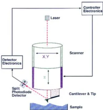
2.2.2 Atomic Force Microscopy ... 26
2.3 Organic dielectric layer deposition and characterization ... 32
2.3.1 Polystyrene and polymethylmethacrylate thin films ... 35
2.3.2 Parylene Vapor Deposition ... 39
2.3.3 Molecular Self Assembled Monolayers on SiO2 ... 42
2.4 Vacuum-sublimation of tetracene thin films ... 46
2.5 Deposition of gold top-contact electrodes ... 52
Chapter 3. RESULTS AND DISCUSSION ... 58
3.1 Nucleation and Growth of Tetracene Thin Films ... 59
3.1.1 Introduction: the role of the early stages ... 60
3.1.2 General considerations on the growth of organic films ... 61
3.1.3 The early stages of tetracene growth ... 63
3.1.4 Island growth and coalescence ... 70
3.1.5 Complete coverage tetracene films ... 73
3.2 Results on Tetracene-based OFETs ... 78
3.3 Charge Carrier Transport in Tetracene OFETs - Discussion ... 87
3.4 Electroluminescence from Tetracene Thin Films ... 91
Chapter 4. CONCLUSION AND PERSPECTIVES ... 94
OTHER WORKS AND PROJECTS ... 97
REFERENCES ... 99
LIST OF TABLES
Table 2.1 – Properties of the organic dielectric layers employed in this project. ... 34 Table 2.2 – Total capacitance of the dielectric bilayers employed in this project. ... 34 Table 2.3 – Some properties of parylene N, C, and D [74]. ... 40 Table 2.4 – Thickness and deposition rate of tetracene in the plane of the sample-holder (at the
center, at 2, and at 5 cm from the center) and corresponding values at the QCM. ... 51 Table 2.5 - Thickness and deposition rate of gold in the plane of the sample-holder (at the center,
at 2, and at 5 cm from the center) and corresponding values at the QCM. ... 54 Table 3.1 – Values of the surface energy for the dielectric substrates investigated in this project,
extracted from the literature [79, 101] and from polymer properties’ databases [102-103]. . 63 Table 3.2 – Properties of the sub-monolayer tetracene films (nominal thickness 2 nm, deposition
rate 3.5 Å/s) calculated by means of WSxM software. Average values and error bars were evaluated from four different AFM images. A set of 15 µm × 15 µm AFM images where the tetracene islands were identified and characterized, is reported below the table. ... 67 Table 3.3 – Properties of the sub-monolayer tetracene films (nominal thickness 5 nm, deposition
rate 3.5 Å/s) calculated by means of WSxM software. Average values and error bars were evaluated from four different AFM images. A set of 10 µm × 10 µm AFM images from where the tetracene islands were identified and characterized is reported in the insets of Figure 3.5. ... 67 Table 3.4 – Results of the linear extrapolation in Figure 3.17 (see text). ... 84
LIST OF FIGURES
Figure 1.1 – P-type OFET mobility in organic thin films and single crystals, during the last three decades. Extracted from reference [12]. ... 2 Figure 1.2 – sp2 hybridization of a carbon atom. (Left) In-plane arrangement of the sp2 orbitals;
(right) three dimensional representation of the sp2 and pz orbitals. ... 4 Figure 1.3 – Bottom gate OFET architectures: (a) top contact and (b) bottom contact geometry. .. 7 Figure 1.4 – Schematic illustration of the transistor channel geometry in the case of a top-contact
OFET, employing the substrate as the gate electrode. See text for definition of symbols. ... 7 Figure 1.5 – Schematic representation of a p-type OFET working in accumulation mode. (Green)
p-type semiconductor; (blue) gate dielectric; (red) gate electrode. ... 8 Figure 1.6 – IDS vs. VDS output characteristics of a tetracene-based top-contact OFET for different
VGS biases: 0, -15, -30, -45, -60 V. ... 10 Figure 1.7 – √|IDS| vs. VGS plot of a tetracene OFET. VDS is biased at -60 V. ... 11 Figure 1.8 – |IDS| vs.VGS transfer characteristics of a tetracene OFET. VDS is biased at -60 V. .... 11 Figure 1.9 – Architecture and working principle of a bottom-contact OLEFET (see text for
details). Extracted from reference [9]. ... 12 Figure 1.10 – Structure of the tetracene molecule. (Dark grey) Carbon atoms. (Light grey)
Hydrogen atoms. Extracted from reference [32]. ... 13 Figure 1.11 – Schematic representation of the energy levels of tetracene (HOMO and LUMO) [4]
and the gold work function (WFAu). The device scheme of the tetracene FET is also presented. ... 14 Figure 2.1 – Bottom gate – top contact tetracene OFET with a bilayer gate dielectric. ... 19 Figure 2.2 – Incident and reflected beams and corresponding electric field vectors used in
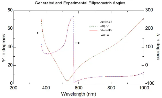
Figure 2.3 – Basic components of an ellipsometer. A known polarization state is changed upon reflection and the final polarization state is measured by the analyzer and the detector. ... 23 Figure 2.4 – Ellipsometric angles measured experimentally (ψ in green and Δ in blue) and
calculated from the theoretical model (red). The curves are relative to a thin layer of PMMA spin coated on a thermally oxidized silicon wafer (ca. 30 nm of PMMA on 200 nm of SiO2 on a Si(100) wafer). A fair overlap between generated and experimental data exists, corresponding to an MSE value equal of 3.61. ... 24 Figure 2.5 – Schematic illustration of the operating principle of an AFM (from Digital
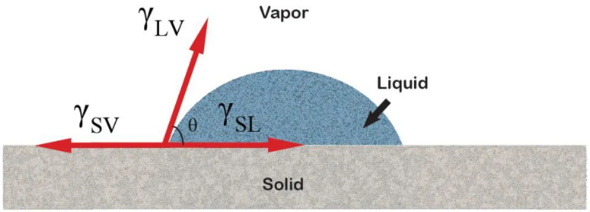
Instruments, Santa Barbara, California). ... 27 Figure 2.6 – Van der Waals force occurring between tip and sample as a function of the tip-sample distance in an AFM microscope. ... 28 Figure 2.7 – Schematic representation of the contact angle θ and illustration of the three surface
tension forces included in the Young’s equation (see text). ... 30 Figure 2.8 – 1 µm × 1 µm AFM images of the dielectric substrate surfaces employed in this
project; height scale: 0 - 3 nm. (a) bare SiO2; (b) PS; (c) PMMA; (d) OTS; (e) HMDS; (f) parylene C. ... 35 Figure 2.9 – PMMA spin-coated on SiO2/Si substrates using the dynamic dispense procedure (see
text for details). ... 37 Figure 2.10 – AFM images of PS thin films deposited on SiO2 on Si substrates; image size 3 µm
× 3 µm; height range: 0 - 3 nm; concentrations: (a) ~3 mg/ml, (b) 5 mg/ml, (c) 10 mg/ml. . 38 Figure 2.11 – Chemical structures of parylene N, C and D. ... 40 Figure 2.12 – Schematic illustration of the Parylene Deposition System (PDS). ... 41 Figure 2.13 – Experimental relationship between film thickness and mass of parylene C inserted
in the vaporizer (see text), employed in this project. ... 41 Figure 2.14 – (Top) SiO2 substrate surface characterized by the presence of siloxanes and silanol
groups. (Bottom) Chemical structures of OTS and HMDS (left) and corresponding SAMs (right). Extracted from reference [80]. ... 43
Figure 2.15 – Schematic illustration of the vapor phase silanization system used in this project. 45 Figure 2.16 – (a) Schematic illustration of the glove-box integrated evaporator and (b)
photograph of the multi-source evaporator for metals and organic molecules used in this project. ... 47 Figure 2.17 – Experimental set-up for tetracene vacuum-sublimation used in this project. ... 49 Figure 2.18 – Layout of the shadow mask used for the realization of the top-contact electrodes.
Size: 18 mm × 18 mm. Thickness: ~250 µm. ... 55 Figure 2.19 – (a) Interdigitated structure of the “second generation” shadow mask for top contact
electrodes in tetracene FETs investigated in this project; (b) Optical microscopy photograph of the effective pattern ablated on the metal foil; (c) optical microscopy photograph of the “third generation” interdigitated structure. ... 56 Figure 2.20 – Three dimensional representation of the final interdigitated top-contact OFET
investigated in this project. ... 57 Figure 3.1 – (Top) Interfacial surface energies involved in the nucleation and growth process of
thin films. (Bottom) Schematic illustration of thin film growth modes: Vollmer-Weber (island growth), Stranski-Krastanov (layer plus island growth) and Frank-van-der-Merwe (layer-by-layer growth). Image extracted from reference [100]. ... 62 Figure 3.2 – AFM images of vacuum sublimed tetracene films with nominal thickness of 2 nm,
deposition rate of 3.5 Å/s. Scale bars denote 1 µm. ... 65 Figure 3.3 – AFM images of vacuum sublimed tetracene films with nominal thickness of 5 nm,
deposition rate of 3.5 Å/s. Scale bars denote 1 µm. ... 65 Figure 3.4 – Particle density (a) and average island surface area (b) for sub-monolayer tetracene
films with nominal thicknesses 2 nm (left) and 5 nm (right). The error bars denote the minimum a maximum value obtained in four distinct AFM images for each substrate. ... 66 Figure 3.5 – Height distribution analysis of sub-monolayer tetracene films (nominal thickness 5
(c) HMDS; (d) parylene C; (e) PS; (f) PMMA. The figure insets represent the AFM images from where the information were extracted. ... 68 Figure 3.6 – 10 µm × 10 µm sized AFM images of tetracene thin films (nominal thickness 10 nm,
deposition rate 3.5 Å/s) grown on different dielectric layers: (a) bare SiO2; (b) OTS; (c) HMDS; (d) parylene C; (e) PS; (f) PMMA. Height scale: 0 - 50 nm. ... 71 Figure 3.7 – Fluorescence images of tetracene films (nominal thickness 17 nm, deposition rate
3.5 Å/s) grown on different dielectric layers: (a) bare SiO2; (b) OTS; (c) HMDS; (d) parylene C; (e) PS; (f) PMMA. The figure insets show 10 µm × 10 µm sized AFM images of the same films, height scale: 0 - 50 nm. ... 72 Figure 3.8 – AFM images of tetracene films with nominal thickness 35 nm, deposition rate 3.5
Å/s. Scale bars denote 1 µm. ... 73 Figure 3.9 – 5 µm × 5 µm sized AFM images of tetracene films with nominal thickness 35 nm,
deposition rate 3.5 Å/s, deposited on different dielectric substrates. ... 74 Figure 3.10 – 5 µm × 5 µm sized AFM images of tetracene films with nominal thickness 50 nm,
deposition rate 3.5 Å/s, deposited on different dielectric substrates. ... 74 Figure 3.11 – PSD analysis of the AFM images presented in Figure 3.9. The intersection between
the “plateau” and the exponential decay (logarithmic scale) represents the reciprocal of the correlation length ε. ... 76 Figure 3.12 – Correlation Length ε (a) and RMS roughness (b) of the AFM images reported in
Figure 3.9. The error bars denote the minimum a maximum value obtained in four distinct AFM images per each substrate. ... 77 Figure 3.13 – Correlation Length ε (a) and RMS roughness (b) of the AFM images reported in
Figure 3.10. The error bars denote the minimum a maximum value obtained in four distinct AFM images per each substrate. ... 78 Figure 3.14 – Drain-source current (IDS) vs. drain-source voltage (VDS) output characteristics at
different gate-source biases (VGS), for tetracene OFETs employing different organic dielectric layers: (a) bare SiO2; (b) OTS; (c) HMDS; (d) parylene C; (e) PS; (f) PMMA. All
curves refer to single-channel devices, with channel length L=100 μm and channel width W = 4000 μm. ... 80 Figure 3.15 – IDS vs. VGS (blue) and √|IDS| vs. VGS (orange) curves, with VDS biased at -60 V, for
tetracene OFETs (L = 100 µm and W = 4000 µm) employing different dielectric layers: (a) bare SiO2; (b) OTS; (c) HMDS; (d) parylene C; (e) PS; (f) PMMA. ... 81 Figure 3.16 – FET mobility extracted from the transfer curves at saturation of tetracene OFETs.
For each type of dielectric layer, different single-channel devices were tested, with L of 60, 80, 100, 150 µm and W of 2 and 4 mm. ... 82 Figure 3.17 – Transmission Line Plot (RTOT∙W vs. L) at VGS = -60 V (black) and VGS = -45 V
(blue) for top-contact tetracene OFETs employing PMMA as organic dielectric layer. The y-axis intercept represents the device contact resistance [87]. ... 83 Figure 3.19 – FET extracted from the saturated transfer characteristics of tetracene-based OFETs
employing different dielectrics. The error bars denote the minimum a maximum value obtained in the devices in Figure 3.16. ... 85 Figure 3.20 – FET Mobility vs. relative dielectric constant for tetracene OFETs fabricated on
different dielectric layers. ... 88 Figure 3.21 – FET Mobility vs. Correlation Length, ε, plot for tetracene thin films with nominal
thickness of 50 nm. The error bars for ε are reported in the histogram of Figure 3.13a. ... 89 Figure 3.22 – (a) Optical image of the circular bottom contact interdigitated electrodes employed
in light emitting tetracene FET investigated in this project; (b) optical image of the electroluminescence generated by tetracene films, under nitrogen atmosphere, showing the light emission region localized close to the negatively biased drain electrode; (c) IDS vs. VGS curves (blue) acquired simultaneously with the photodiode current (orange) caused by the light-emitted by the tetracene FET. W = 41000 µm and L = 6 µm. ... 93
LIST OF ABBREVIATIONS
AFM Atomic Force Microscopy
AM Amplitude Modulation
AMLCD Active Matrix Liquid Crystals Display CVD Chemical Vapor Deposition
DOS Density of States
F8T2 Poly-9,9’ dioctyl-fluorene-co-bithiophene FET Field Effect Transistor
FFT Fast Fourier Transform
FM Frequency Modulation
HMDS Hexamethyldisilazane
HOMO Highest Occupied Molecular Orbital LUMO Lowest Unoccupied Molecular Orbital MEMS Micro-Electro-Mechanical System
MOSFET Metal Oxide Semiconductor Field Effect Transistor MSE Mean Square Error
OLEFET Organic Light Emitting Field Effect Transistor OLED Organic Light Emitting Diode
OFET Organic Field Effect Transistor OS Organic Semiconductor
OTFT Organic Thin Film Transistor OTS Octadecylthrichlorosilane P3HT Poly (3-Hexylthiophene)
PARY-C Poly(monochloro-p-xyllyene) PDS Parylene Deposition System PMMA Polymethylmethacrylate PPV Poly(p-phenylene vinylene)
PS Polystyrene
PSD Power Spectral Density PVD Physical Vapor Deposition QCM Quartz Crystal Microbalance RMS Root Mean Square
RFID Radio Frequency Identification SAM Self Assembled Monolayer SCA Single Curve Analysis SPM Scanning Probe Microscopy STM Scanning Tunnelling Microscopy TLM Transfer Line Method
Chapter 1.
INTRODUCTION
1.1 Historical perspective and motivation
It has long been a widespread idea that organic materials are electrical insulators. In 1977 A. J. Heeger, A. G. MacDiarmid and H. Shirakawa, discovered that the electrical conductivity of polyacetylene could be dramatically increased (up to eleven orders of magnitude) by chemical doping and showed to the world the possibility to synthesize conducting plastics [1-2]. For this discovery, they were awarded the Nobel Prize for Chemistry in 2000. It represented a breakthrough in the field of organic materials and marked the beginning of a new research field focused on electrically conducting organic polymers and molecules.
After this discovery, scientists were mainly interested in polymers with “metallic” behavior and hence little research was carried out on the semiconducting properties of organic polymers and molecules. From the historical point of view, the first investigations of Organic Semiconductor (OS) molecules date back to the beginning of the 20th century, as witnessed by the pioneering works of the Italian scientist A. Pochettino [3], who discovered and studied the photoconduction mechanism in crystals of anthracene. Electroluminescence and photovoltaic effects in π-conjugated small molecules and polymers, where the molecular structure is characterized by the presence of alternate single and double bonds, were demonstrated by the half of the century [4]. For the first time in 1964 a field-dependent electrical conduction was observed in thin films of phthalocyanines [5]. However, until the late 1980s, research on OSs was far from being satisfactory and no practical applications were demonstrated.
An important step occurred in 1986, when Koezuka and Tsumura demonstrated the first Organic Field Effect Transistor (OFET) based on an electrochemically polymerized polythiophene thin-film [6]. This demonstration opened the possibility to fabricate organic electronic circuits and started the era of “organic electronics”, enabling for a series of significant technological applications, such as flexible field-driven displays, logic circuits, chemical and mechanical sensors, image sensing devices and Radio Frequency Identification (RFID) tags [7].
Nowadays, a number of OS, both polymers and small molecules, have been synthesized and commercialized [8] and new OFET architectures have been designed to exploit the functionalities of these materials.
The great interest in organic electronics is motivated by the unique characteristics of OSs, such as the possibility to conveniently tailor their optoelectronic properties (e.g. optical band gap) by means of chemical synthesis, low-cost processing, compatibility with flexible plastic substrates and biocompatibility [9]. Differently from the conventional inorganic semiconductors employed in the electronic industry, OSs do not necessarily require any expensive under-vacuum and high-temperature processes but can be deposited with low-cost methods, such as solution cast, inkjet and micro-contact printing [10]. The mechanical flexibility of organic materials and their low processing temperature allow for using low-cost and flexible substrates, such as glasses, plastics and metal foils [11]. In turn, this enables for fabricating large-area/roll-up displays (e.g. electronic newspaper) and photovoltaic panels.
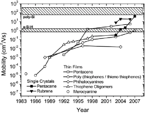
Since the first devices – characterized by a mobility of 10-5 cm2V-1s-1 – OFETs have known an extraordinary increase in mobility (more than six orders of magnitude), as shown in Figure 1.1.
Figure 1.1 – P-type OFET mobility in organic thin films and single crystals, during the last three decades. Extracted from reference [12].
Hence, nowadays, the OFET technology is mature enough to compete with amorphous and polycrystalline silicon (a-Si:H and poly-Si) technologies, e.g. in Active Matrix Liquid Crystals Displays (AMLCD) backplanes. However, as pointed out in [13], organic electronics will never replace the well established Si electronics, which will continue to keep a dominant role in the microprocessor industry. The charge carrier mobility in single crystals of the most common inorganic semiconductors (Si, Ge, GaAs), is at least three orders of magnitude larger than in the best performing OS. Instead of this, organic electronics is expected to complement and extend it in applications where high switching speed is not a requirement and where low costs, biocompatibility, large and flexible substrates represent a priority.
Beyond OFETs, which are devices used to switch and modulate electronic signals, current research in organic electronics includes light-emitting devices, such as Organic Light Emitting Diodes (OLEDs) and photo-absorption devices, such as solar cells and photodetectors. In 2003, a new class of organic devices has been demonstrated, i.e. Organic Light Emitting Field Effect Transistors (OLEFETs) which represent the smallest possible integration of the light emission function of the OLED with the current modulation function of the OFET [14].
OLEFETs are interesting from a technological standpoint, due to the many applications envisaged, such as active matrix full-color displays, optical communication devices, solid-state lighting and ultimately organic injection lasers [9, 15]. Moreover, due to their planar geometry (see Section 1.4), as opposite to the vertically stacked geometry of OLEDs, they offer direct access to optical probes thus opening the possibility for investigating fundamental processes in OSs, such as excitons formation, recombination and light emission [15]. High-performance OLEFETs have been recently demonstrated with an efficiency higher than the equivalent OLEDs [16], suggesting that the promises related to this technology are not far from becoming reality. However, much work is left to do to fully understand the aspects that influence the performance of OLEFETs. This project aims to shed light on the role of the dielectric surface (Section 1.3 and Section 1.4) in influencing the charge transport properties of organic thin films to be incorporated in OLEFETs.
1.2 Organic semiconductors: an overview
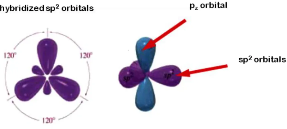
OSs are carbon based polymers and small molecules where adjacent carbon atoms are linked together by alternate single and double bonds. The carbon atoms of an OS are hybridized in the sp2 configuration, as shown in Figure 1.2. The σ-bonds, formed by the overlap of the sp2 orbitals of two adjacent carbon atoms, constitute the backbone of the molecule. On the other hand, the π-bonds result from the overlap of the pz orbitals of two adjacent carbon atoms and are weaker than the σ bonds. The pz orbitals of all the carbon atoms in the OS combine to form a delocalized electronic orbital spread over the entire backbone of the molecule. The resulting electronic structure is referred to as a π-conjugated electronic system, which is peculiar to all OSs, both polymers and small molecules [17].
Figure 1.2 – sp2 hybridization of a carbon atom. (Left) In-plane arrangement of the sp2 orbitals; (right) three dimensional representation of the sp2 and pz orbitals.
Small molecules can form single crystals and thin films and are commonly deposited by Physical Vapor Deposition (PVD) techniques. Polymers, on the other hand, can be deposited only in the form of thin films, by the use of solution processing techniques. This stems from the fact that thermal evaporation induces their degradation.
The electronic structure of all OSs is characterized by the presence of a relatively large energy gap (usually 2 - 3 eV [18]) between the energies of two molecular orbitals, the Highest Occupied Molecular Orbital (HOMO) and of the Lowest Unoccupied Molecular Orbital (LUMO). These are analogous to the edges of the valence and conduction band respectively of conventional inorganic semiconductors [19].
Thin films and single crystals of OSs are often investigated as active materials in Field Effect Transistors (FET), which provide a straightforward configuration to study their charge transport properties [18]. Several OSs, when incorporated in OFETs (see Section 1.3), show accumulation of positive charges (holes) in the transistor channel upon application of a negative gate bias. The opposite process, i.e. accumulation of negative charges (electrons) upon application of a positive gate bias, is less frequently observed [19]. When holes are accumulated and transported inside the transistor channel, the OS is referred to as “p-type”. On the other hand, when electrons are accumulated and transported, the OS is referred to as “n-type”.
Nowadays, several high-performance p-type OSs are commercially available, but the same is not true for the n-type counterpart. The development of high-performance n-type materials is challenging [8] and it is regarded as the key step towards the fabrication of complementary transistor circuits (CMOS-type), for application in organic digital electronics [19].
The “type” of an OS depends on its chemical structure, so that chemical synthesis processes have been intensively studied to develop new p-type and n-type materials starting from pre-existing OSs. For example, from a common core unit, such as a thiophenes oligomer, it is possible to obtain both p-type and n-type materials by adding electron-accepting or electron-donating groups, as reported in reference [20].
The possibility for n-type or p-type conduction does not depend only on the chemical structure of the OS but also on other aspects related to both the semiconductor deposition/processing conditions and the device architecture/components (we refer to Section 1.3 for the description of the OFET). It is known that the source and drain electrodes materials as well as the dielectric layer surface chemistry play a crucial role in establishing a p-type or n-type transport. As pointed out in [8, 18], one should not refer to an OS as p-type or n-type, but rather should apply this classification to the transistor channel.
A key step in the knowledge of OSs and related devices was taken in 2005, when Chua et al. proved that the use of hydroxyl free gate dielectrics – instead of the commonly employed SiO2 dielectric – enabled the n-type transport in a number of polymeric OSs that were previously believed to be exclusively p-type [21]. This discovery paved the way towards the observation of n-type transport at first in a number of semiconducting polymers and afterward in small molecules [22], seeming to confirm the hypothesis that organic semiconductors are in principle
“intrinsically ambipolar”, i.e. capable to transport – under specific device configurations and processing conditions – both electrons and holes [18]. Reasons for the commonly observed n-type conduction suppression were individuated in the electron trapping mechanisms associated to the silanol groups present on the SiO2 surface. Recently, it was shown that the electron transport suppression is more in general induced by an electrochemical charge transfer processes between the semiconducting channel and the red-ox couple system of an adsorbed water/oxygen layer [23]. The adsorption of the oxygen/water layer is favored by the presence of hydrophilic groups (e.g. silanols) on the dielectric substrate surface. It can be limited by hydrophobic groups, such as for example polymer layers and Self Assembled Monolayers (e.g. octadecyltrichlorosilane, OTS). Ambipolarity is a critical property from a technological standpoint, for the fabrication of complementary transistor circuits based on a single organic semiconducting material. This would imply the possibility to conveniently fabricate logic gates without the requirement to pattern two different OSs. Moreover, ambipolarity is a fundamental property for the realization of high-performance OLEFETs, where efficient light emission is possible only if excitons (bound electron-hole pairs) are formed inside the transistor channel, far from metal electrodes.
In the following sections we introduce the architecture and the working principle of OFETs (Section 1.3) and OLEFETs (Section 1.4), which are the devices under study in this research project.
1.3 Organic Field-Effect Transistors
Organic Field Effect Transistors (OFETs) are devices constituted by five distinct components. A gate electrode (i) is separated from the active OS (ii) by the gate dielectric (iii). In bottom gate transistors, schematically represented in Figure 1.3, the source (iv) and drain (v) electrodes can be positioned either on top of the OS (top contacts, Figure 1.3a) or on the gate dielectric (bottom contacts, Figure 1.3b).
In OFETs, the transistor channel is located at the interface between the dielectric layer and the OS and extends only for a few nanometers in the direction orthogonal to the interface [24]. For this reason, the bottom contact geometry is referred to as “coplanar”, in the sense that both the electrodes and the transistor channel lie on the same plane. On the contrary, the top contact
geometry is referred to as “staggered”, since the source and drain electrodes do not contact directly the transistor channel but lie above it [25].
Figure 1.3 – Bottom gate OFET architectures: (a) top contact and (b) bottom contact geometry. The geometry of the transistor channel is characterized by the inter-electrode distance L and the electrode width W, as represented in Figure 1.4.
Figure 1.4 – Schematic illustration of the transistor channel geometry in the case of a top-contact OFET, employing the substrate as the gate electrode. See text for definition of symbols.
The working mechanism of OFETs can be described by means of the long-channel silicon device model [7, 26], that is based on the gradual channel approximation. This requires that the electric field induced by the gate electrode in the direction orthogonal to the current flow is much larger than the electric field induced by the source and drain electrodes in the direction parallel to the current flow. This condition is generally satisfied when the channel length L is much larger than the thickness of the insulating layer ti (L > 10∙ ti) [18] and is essential for having OFETs with current-voltage characteristics that could be described by the equations of the long-channel silicon device model (vide infra). Only under this condition it is possible to extract the correct
field effect mobility µ, which represents the charge carrier drift velocity per unit of electric field strength. The model requires also that the charge carrier mobility is constant over all the transistor channel.
OFETs work in accumulation mode and therefore the polarity of the transistor channel is the same as the polarity of the majority carriers in the OS. In addition, it is not possible to define the threshold voltage (Vth), similarly to the case of MOSFETs, as the gate voltage necessary to achieve the inversion regime [26]. In OFETs there is not a depletion layer and thus, ideally, the threshold voltage should be zero [27]. However, this condition is never satisfied and a non vanishing voltage has to be applied to the gate to induce a significant current flow between the source and drain electrodes. As pointed out in [7], in the context of OFETs there is not a unique and rigorous definition of threshold voltage. Generally, the threshold voltage is described as the gate voltage required to achieve the “onset of accumulation”.
In the following discussion, we refer to OFETs based on p-type OSs. Basically, an OFET can be regarded as a capacitor where the two plates are (i) the gate electrode and (ii) the OS, separated by the gate dielectric. The source electrode is usually grounded. When a negative voltage VGS is applied between the source and gate electrodes, as in Figure 1.5, mobile charge carriers (holes) are drawn into the transistor channel and are accumulated at the semiconductor/dielectric interface. If a negative voltage VDS is applied between source and drain, an electric current IDS starts to flow between the two electrodes. Under the effect of the VDS bias, the holes injected from the source electrode into the HOMO level of the OS, move towards the drain electrode where they are finally collected.
Figure 1.5 – Schematic representation of a p-type OFET working in accumulation mode. (Green) p-type semiconductor; (blue) gate dielectric; (red) gate electrode.
The magnitude of the transistor current flowing between the source and drain electrodes is modulated by the gate voltage VGS. Ideally, with no bias applied to the gate, the current should be nil; however a non vanishing current, (IOFF) is measured in all OFETs.
The long channel silicon device model deals with three different regimes of operation. When the gate voltage is lower than the threshold voltage Vth, there are few mobile carriers in the transistor channel and no current flows between the drain an source electrodes. The device is said to be in “cut-off ”:
At small VDS and large VGS the device is in the “linear regime” and the current-voltage relation is given by the following equation.
where Ci is the capacitance of the gate dielectric. By increasing VDS, a condition can be achieved in
which the potential drop between the transistor channel and the gate electrode becomes smaller than the threshold voltage. This condition is satisfied in close proximity to the drain electrode when VDS = VGS - Vth. The channel becomes “pinched-off ” and a region is formed at the “pinch-off” point where no significant concentration of mobile charge carriers are accumulated at the dielectric/semiconductor interface. This limits the rate of current increase and causes the current to saturate [7]. The value of IDS in the “saturation regime” is obtained by evaluating the (1.2) at VDS = VGS - Vth :
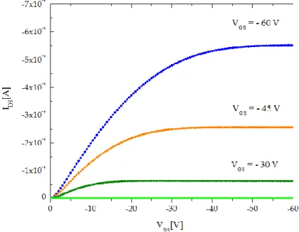
The drain-source current IDS can be measured and plotted either by varying the drain-source voltage VDS and keeping constant the gate-source voltage VGS (output curves, Figure 1.6) or by varying VGS and keeping constant VDS (transfer curves, Figure 1.7 and Figure 1.8). An example of output characteristics, obtained from the top-contact tetracene OFETs fabricated in this research project is shown in Figure 1.6.
The figures of merit of OFETs are the threshold voltage Vth, the FET mobility µ, the ratio, and the sub-threshold slope. The threshold voltage is commonly obtained from the
saturated transfer characteristics (at large constant VDS) as the X-axis intercept of the linear extrapolation of the √|IDS| vs. VGS, as shown in Figure 1.7.
Figure 1.6 – IDS vs. VDS output characteristics of a tetracene-based top-contact OFET for different VGS biases: 0, -15, -30, -45, -60 V.
The mobility is commonly extracted in the saturation regime. In this way, possible non linear effects that may influence the transistor behavior at small drain-source voltages, such as non-ohmic contacts (injection barriers due to the mismatch between the HOMO/LUMO of the OS and the work function of the electrode), do not affect the mobility measurement.
The FET mobility µ is calculated using the following formula, which is derived from the (1.3):
where
is the slope of the linear extrapolation of the √|IDS| vs. VGS plot (Figure 1.7).
The sub-threshold slope is obtained from the saturated transfer characteristics and is defined as the inverse slope of the log(|IDS|) vs. VGS curve at large constant VDS, as indicated in Figure 1.8. The sub-threshold slope is related to the device switching speed: the smaller the sub-threshold slope, the faster the transition between the ON and the OFF states. Typical values of the sub-threshold slope for the tetracene OFETs fabricated in this project are in the range 1-3 V/dec.
ION/IOFF is defined as the ratio between the maximum current in the ON state (ION) and the minimum current in the cut-off regime (IOFF). It is evaluated from the saturated transfer characteristics at large constant VDS, as shown in Figure 1.8. The tetracene OFETs fabricated in this research project had a ION/IOFF value included in the range 105 – 106.
Figure 1.7 – √|IDS| vs. VGS plot of a tetracene OFET. VDS is biased at -60 V.
1.4 Organic Light Emitting Field Effect Transistors
OLEFETs, whose structure and working principle are shown in Figure 1.9, integrate the switching function of the transistor with light emission and are attractive for both fundamental studies and technological applications. Differently from OLEDs, where the OS is sandwiched between the anode and cathode electrodes, the planar geometry of the OLEFET offers direct access to optical probes and permits a direct imaging of the electroluminescence generated by the OS. Hence, OLEFETs can be conveniently used as test systems to investigate fundamental physical processes in OSs, as mentioned in Section 1.1. The OLEFET of Figure 1.8 corresponds to a bottom gate – bottom contact OFET, where the organic semiconducting film is deposited on substrates with pre-patterned source and drain electrodes.
Figure 1.9 – Architecture and working principle of a bottom-contact OLEFET (see text for details). Extracted from reference [9].
Notice that other OLEFET geometries are possible, among which the bottom gate – top contact (Figure 1.3a) geometry is among the most commonly employed (e.g. [16]), since it allows for an ad hoc preparation/treatment of the dielectric substrates surface. For the same reason, a bottom gate – top contact architecture was employed in the context of this research project.
The working mechanism of an OLEFET stems from that of the corresponding OFET (Section 1.3). When an appropriate bias VGS is applied to the gate, holes and electrons are injected from the source and the drain and are accumulated in the transistor channel, where they move under the action of a drain-source bias (VDS). If the OS is electroluminescent, holes and electrons form
excitons that recombine radiatively and generate light. The current (IDS) flowing between source and drain and the intensity of the light emitted from the OLEFET are modulated by VGS, which is also used to switch the device between the OFF (dark) and the ON state (light). Hence, OLEFETs can be indeed regarded as self-driven light-emitting devices.
The first OLEFETs were based on unipolar OSs, but their efficiency was low due to the localization of the light emission region in the proximity of the minority charge carrier-injecting metal electrode, which causes light emission quenching. Nowadays, high efficiency OLEFETs based on ambipolar materials have been demonstrated: the light emission region can be moved far from the metal electrodes; the position inside the transistor channel where excitons form and recombine, can be easily controlled by varying the gate voltage VGS and the drain-source voltage VDS [28]. This allows limiting metal quenching effects and thus improving the light emission efficiency.
1.5 Tetracene-based OLEFETs
The first prototype of OLEFET was based on polycrystalline films of tetracene, a π-conjugated small molecule constituted by four fused benzene rings (Figure 1.10). Tetracene, a commercially available p-type OS, is characterized by both good charge transport properties and relatively high fluorescence quantum yield [29]. The hole mobility can be as high as 2.4 and 0.1 cm2V-1s-1 in single crystals and polycrystalline films, respectively [30-31].
Figure 1.10 – Structure of the tetracene molecule. (Dark grey) Carbon atoms. (Light grey) Hydrogen atoms. Extracted from reference [32].