Introduction
The development of organic fi eld-effect transistors (FETs) based on conjugated molecules or polymers is driven by applications in the fi eld of plastic electronics, 1–7 in which molecular semi-conductors are used to produce large-area, low-cost, fl exible electronic devices. These devices also provide an ideal setting for the development of a basic understanding of the micro-scopic physical mechanisms associated with charge transport in organic semiconductors. For instance, it is not well understood why some molecules lead to charge-carrier mobilities that are much larger than those for others. When compared to inorganic semiconductors such as silicon or III–V compounds, it seems clear that technology based on organic semiconductors would vastly benefi t from a much more systematic, basic understand-ing of the electronic properties of these materials.
Investigating the intrinsic transport properties of organic semiconductors and their interfaces, which determine the tran-sistor performance, requires materials of the highest quality to minimize extrinsic effects. Research groups have been pursuing the study of FETs based on single crystals of organic conjugated
molecules, 8–18 which are now setting benchmarks for the
performance of organic FETs. Single-crystal devices have led to observations of new physical phenomena and to the exploration of molecular materials that are pushing the limits of organic electronics beyond what had been initially foreseen. Here we provide a short introduction to the fi eld, with special focus on the interplay between the transport properties of organic
semiconductors and the physics of organic devices. In doing so, we also discuss the microscopic mechanisms that determine charge-carrier motion in these systems.
Fabrication of organic single-crystal transistors
A variety of techniques are used to realize FETs 19 based on organic single crystals. Crystals can be grown directly on substrates, for instance, by letting a drop-casted solution containing mole-cules evaporate, 20 or by seeding (vapor-phase) crystal growth at controlled locations. 21 The most common fabrication technique,however, separates crystal growth and transistor assembly. 19
A common strategy relies on manual lamination (see Figure 1 ) of organic crystals grown from vapor phase onto a substrate, in which the gate, source, and drain contacts are fabricated prior to lamination. 8,10,11 One can choose between a solid con-ducting substrate (acting as a gate) coated with a dielectric of choice, 8,10,11,18,19 or elastomer stamps 22,23 covered with a metal layer, molded to form the source and drain electrodes, and a recessed gate (so that air or vacuum acts as a dielectric). These latter devices show the largest mobility values and highest quality, as manifested by the observation of a band-like temperature
dependence of the carrier mobility 24 (see below for more
details on band-like transport). Techniques of this type have been applied to a broad variety of different molecular crystals to investigate both p- and n- channel devices 23–27 (see Figure 1 ).
Separating crystal growth and device assembly represents an advantage that can hardly be over-emphasized. Laminating
effect transistors
Ignacio Gutiérrez Lezama and Alberto F. Morpurgo
Research on organic thin-fi lm transistors tends to focus on improvements in device performance, but very little is understood about the ultimate limits of these devices, the microscopic physical mechanisms responsible for their limitations, and, more generally, the intrinsic transport properties of organic semiconductors. These topics are now being investigated through the study of transport in organic transistors realized using molecular single crystals of unprecedented chemical purity and structural quality. These studies are elucidating detailed microscopic aspects of the physics of organic semiconductors and corresponding devices and have also led to unforeseen high values for carrier mobility in these materials. Here, we discuss developments in this area and present a brief outlook on future goals that have come into experimental reach.
Ignacio Gutiérrez Lezama, Department of Condensed Matter Physics , École de Physique , Geneva , Switzerland ; [email protected] Alberto F. Morpurgo, Department of Condensed Matter Physics , École de Physique , Geneva , Switzerland ; [email protected] DOI: 10.1557/mrs.2012.311
previously grown crystals ensures that the quality of the organic material is always the same, which facilitates the correlation of device structure to performance. This is not possible for thin-fi lm transistors, where the performance of FETs based on the same molecule frequently varies due to, for example, variations in thin-fi lm morphology. In the investigation of the contact resistance, for instance, molecules deposited on the metal electrodes and on the dielectric (i.e., the channel) pack differently—resulting in grain boundaries, 28 – 30 whose effects on transport could not be separated experimentally from those of the metal/semiconductor interface. Organic single-crystal FETs realized by lamination offer high device-to-device repro-ducibility and have enabled the systematic investigation of mobility anisotropy, 23 , 31 , 32 the infl uence of the gate dielectric on the mobility, 33 , 34 bias-dependent contact resistance, 35 , 36 and
charge-transfer at metal-organic interfaces. 37 Even though
lamination on SiO 2 wafers or polydimethylsiloxane (PDMS)
stamps is typically performed in ambient conditions, experi-ments indicate that interfacial contamination does not notably
affect the electronic properties of the resultant single-crystal devices, which show a surprising reproducibility. 38 This is likely due to the hydro-phobic nature of smooth surfaces of molecu-lar crystals with no grain boundaries or other defects that usually facilitate physisorption and chemisorption of contaminants.
Device electrostatics
In semiconducting devices, electrostatics deter-mines the local density of charge carriers and plays a dominant role 39 that needs to be under-stood in order to correctly describe and interpret transport experiments. This point is illustrated by the behavior of space-charge limited
cur-rent, 40 where seemingly minor perturbations
(e.g., small densities of surface traps) can dras-tically affect the electrostatic profi le. 41 , 42 From the viewpoint of electrostatics, even though it makes no difference if a transistor is realized using an organic or a conventional semiconduc-tor (e.g., silicon), some important differences remain when it comes to the underlying device physics. In contrast to commonly used inorganic semiconductors, organic semiconductors are undoped, and one may wonder whether this difference invalidates conventional theory established for silicon FETs. The formation of a Schottky barrier at a metal/semiconductor inter-face, for instance, originates from the electro-static profi le of the bands in the semiconductor that is determined by the dopant density, 39 and it has long remained an open question whether the conventional Schottky theory 39 , 43 , 44 applies to organic materials. To settle such questions, it is important to discriminate—in experiments— new physical phenomena that may occur in organic semiconductors from other unrelated effects. In organic thin-fi lm transistors, the situation is more complicated because the pres-ence of grain boundaries affects the electrostatics, often leading to either irreproducible or unconventional device behavior, which is at odds with established theory. 28 – 30 Organic single-crystal devices, on the contrary, are rather immune to these shortcomings.
A series of experiments on rubrene single-crystal FETs has examined the degree to which device electrostatics conform to the behavior expected for conventional inorganic transistors. These include the study of short-channel FETs 35 , 36 and
Schottky-gated transistors 45 (so-called MESFETs). Owing to the high
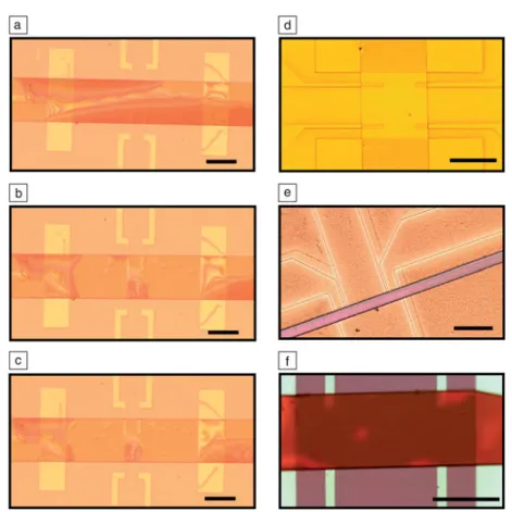
carrier mobility, the resistance of short-channel devices (see Figure 2 a) is dominated by the metal/semiconductor interfaces and can be modeled as two oppositely biased Schottky diodes. 35 The measurements directly give information about the Schottky barrier height and its electric fi eld dependence (i.e., the Schottky effect). In devices with copper electrodes, 36 it was found that Figure 1. (a–c) Optical micrographs illustrating the time evolution of the spontaneous
adhesion of a rubrene single crystal to an SiO 2 substrate during lamination. 19 (d–f) Optical
micrographs offering a top view of several single-crystal fi eld-effect transistors. (d) Rubrene singe crystal laminated on top of a polydimethylsiloxane stamp covered with a gold layer. The gate electrode is recessed, hence vacuum acts as the dielectric. 34 (e) Similar
device as in (d) made with a tetramethyl tetraselena fulvalene single crystal. 26 (f) N,N ′ -bis
( n -alkyl)-(1,7 and 1,6)-dicyanoperylene-3,4:9,10-bis(dicarboximide), n -type single-crystal laminated onto a cytop (amorphous fl uoropolymer) fi lm. 27 The scale bars in (a–e) are 200 μ m;
the conventional theory of transport through a Schottky bar-rier 39 , 43 , 44 reproduces the data quantitatively ( Figure 2b–c ), with physically sensible and internally consistent parameters. In the same short-channel transistors used to investigate the Schottky barrier, the analysis is further supported by the study of the length and bias dependence of the threshold voltage 37 associ-ated with the charge transferred from the metal to the organic semiconductor. Quantitative agreement ( Figure 2d ) between experiments and theoretical estimates was found when using the system parameters extracted from the study of the contact resistance and of the MESFET devices (e.g., Schottky barrier height, and density of unintentional dopants present in rubrene), without the need to introduce any additional free parameter. 37 It can therefore be concluded that for FETs realized on organic materials of suffi ciently high structural quality, the device elec-trostatics are correctly described by the conventional theory established for inorganic transistors.
Microscopic physics of organic semiconductors
The fact that the electrostatics of organic and inorganic single-crystal FETs can be described by similar mathematical models does not mean that the underlying microscopic physics of charge transport is the same in the two cases. Most differencesoriginate from the fact that in organic semi-conductors, the constituent molecules are held together by weak van der Waals forces. 46 , 47 The electronic bandwidths associated with the high-est occupied molecular orbital and the lowhigh-est unoccupied molecular orbital are much smaller than in common inorganic semiconductors (a few hundred meV in molecular crystals and approx-imately 10 eV in inorganic semiconductors). A small bandwidth in organic semiconductors implies that charge carriers are very sensitive to interactions 46 , 47 (e.g., with molecular vibrations, other carriers, and disorder). Indeed, the relative impact of such interactions is determined by the ratio of their strength to the relevant bandwidth.
Band-like transport
An important breakthrough enabled by organic single-crystal transistors is the observation 23 – 25 of the so-called band-like transport regime 48 , 49 at fi nite carrier density, with signatures of an increase in mobility with decreasing tempera-ture, 24 – 26 , 50 observation of the Hall effect, 25 , 27 , 51 and an anisotropic mobility. 23 , 31 , 32 A Rutgers University (Podzorov and Gershenson)/University of Illinois (Rogers) collaboration 24 fi rst observed these phenomena in rubrene single-crystal FETs. Band-like transport has been reported in a number of other compounds, for instance in
tetramethyl tetraselena fulvalene (TMTSF), 26
2,7-dioctyl[1] benzothieno[3,2- b ][1] benzo-thiophene (C 8 -BTBT), 50 and N,N ′ -bis( n -alkyl)-(1,7 and 1,6)-dicyanoperylene-3,4:9,10-bis(dicarboximide) (PDIF-CN 2 ) 27 single-crystal devices, both for holes and electrons ( Figure 3 ). For holes, 34 mobility values as high as 20 cm 2 /Vs
at room temperature, increasing to approximately 40 cm 2 /Vs at
150–200 K, have been observed; for electrons, 27 μ ∼ 5 cm 2 /Vs
at room temperature has been observed, reaching ∼ 10 cm 2 /Vs
at 200 K.
These achievements were not foreseen when organic single-crystal FET research started. Room temperature mobility values of 20 cm 2 /Vs 24 , 34 largely exceed what was reported long ago ( ∼ 1 cm 2 /Vs) by Norbert Karl in textbook time-of-fl ight (TOF)
measurements 52 on zone-refi ned single crystals of different
conjugated molecules. Nevertheless, in FETs, the mobility is invariably found to decrease upon lowering temperature below 150–200 K, whereas in the best zone-refi ned organic crystals, the TOF mobility increases down to liquid helium
tempera-ture (reaching values of several 100s cm 2 /Vs). This apparent
inconsistency remains to be understood. Apart from possible differences in the two measurement techniques—TOF probes optically excited carriers whose energy is larger than that of carriers responsible for transport in FETs—the different low-temperature behavior is likely an extrinsic effect due to contamination of the crystal surface, affecting carriers in Figure 2. Transport through short-channel rubrene fi eld-effect transistors with Cu
electrodes. Notice in (a) how many different transistors can easily be realized on a same single crystal. (b) The source/drain current-voltage characteristics ( I SD – V SD ) (symbols) of
these devices, measured at different temperatures ( T ), can be modeled in terms of two oppositely biased Schottky diodes, using the conventional Schottky theory (solid lines). 36
(c) The bias-dependence of the Schottky barrier height ( E A , circles) can also be reproduced
using the same theory 36 (solid line). (d) Short-channel devices show a length-dependent
threshold voltage shift ( δ V T ( L ), circles) due to charge-transfer from the metal contacts,
which becomes non-negligible for submicron channel lengths ( L ). 37 The length dependence
of the threshold voltage can be accounted for quantitatively using the known range of Schottky barrier heights, 0.13 eV (dashed line) and 0.15 eV (solid line) obtained from the study of the contact resistance performed on the same devices.
the transistor channel but not in TOF experiments (which probe the bulk).
Microscopically, the nature of band-like transport in organic FETs is not yet understood, although, theoretical progress has been made. 48 , 49 , 53 – 56 An important step was to
realize that at room temperature, molecular motion (rotations and vibrations) leads to large fl uctuations in the hopping integrals (the matrix elements of the charge carrier Hamiltonian between states at neighboring sites), which are of the order of the equilibrium values. 54 Charge carriers respond on a time scale much faster than the molecular motion and experience the random, thermally induced molecular confi gurations as a very strong disorder causing Anderson localiza-tion (i.e., a complete localizalocaliza-tion of the carrier wave function due to quantum interference). On a longer time scale, the molecular confi gu-ration changes, and the localized carriers diffuse “following” the molecular motion. The mobility increases with lowering temperature because at lower T , the amplitude of the molecular motion decreases, and the localization length increases. 49 , 54 – 56 Since in the temperature range investigated the localization length is never much larger than the lattice spacing, such a regime is different from true band transport, expected to occur only at much lower T (in actual materials, however, extrinsic disorder takes over, causing “static” carrier localization and a steep decrease of the fi eld-effect mobility). While there is con-sensus that this scenario is physically correct for
high-purity organic single-crystal FETs, the problem remains diffi cult to treat theoretically because several important energy scales have a comparable magnitude: 47 , 49 the bandwidth, its fl uc-tuations due to molecular motion, temperature, and disorder. It is important to develop theoretical schemes enabling controlled approximations to systematically address this transport regime.
Charge carriers and their dielectric environment
Considerable progress has been made in understanding the interaction between charge carriers in the FET channel and the nearby gate dielectric. 33 , 34 , 57 – 61 Apart from chemical groups present at the dielectric surface acting as traps (very important, especially for electron transport 62 ), the electrical polarizability of the gate insulator plays a key role. 33 , 34 , 57 If the polarizability is large and originates from slow (compared to the charac-teristic electronic times) degrees of freedom, charge carriers couple strongly to the polarization cloud that they themselves induce in the dielectric (in simple terms, their image charge). This coupling amplifi es the trend of the charge carriers toward localization, and it is observed experimentally 34 that a cross-over occurs from band-like transport to thermally activated hopping upon increasing the polarizability of the dielectric ( Figure 4 ). In the strong coupling regime, the observations can be quantitatively described in terms of polaron formation—a quasiparticle formed by the coupling of a charge carrier to the electrical polarizability of the surrounding medium—using a well-defi ned microscopic theory that could be extended to Figure 3. Band-like transport in single-crystal
fi eld-effect transistors laminated on top of gold-covered polydimethylsiloxane stamps (similar to those shown in Figure 1 ), in which single crystals of tetramethyl tetraselena fulvalene (TMTSF), 26 N,N ′ -bis( n -alkyl)-(1,7 and
1,6)-dicyanoperylene-3,4:9,10-bis(dicarboximide) (PDIF-CN 2 ), 27
and rubrene 34 are suspended above a gate electrode. At low
temperatures, the mobility ( μ ) decreases as temperature ( T ) is lowered due to disorder-induced trapping of charge carriers (not shown for rubrene).
Figure 4. Infl uence of the gate dielectric on charge-carrier mobility ( μ ) and its temperature
dependence ( T ), as measured on rubrene single crystals with different gate insulators. 33 , 34
(a) At room temperature, the carrier mobility decreases with increasing dielectric constant ( ε ), while a crossover from band-like transport to thermally activated hopping is observed in the temperature dependence, as shown in (b) by the decrease of the mobility with decreasing temperature in transistors with higher gate dielectric constants. Note: PDMS, polymethylsiloxane. (c) Schematic view of how holes accumulated in the transistor channel—at the organic/dielectric interface—polarize the gate dielectric. 34
explain the high carrier density regime, with non-negligible Coulomb interactions between carriers. 61 , 63 Coulomb interac-tions cause the FET conductivity to saturate at large carrier density, because mutual Coulomb repulsion suppresses polaron hopping. Organic single-crystal FETs have therefore enabled controlled investigations of polaron physics at low and high carrier densities (see also the article by Xie and Frisbie in this issue).
The coupling to the gate dielectric remains important even when the polarizability is small, as in polymeric insulators. True interfacial polarons do not form in this case. The interaction is better described in terms of the phenomenological concept of “dipolar disorder” originally introduced by Veres, 57 , 58 who stud-ied hopping transport in devices based on disordered conjugated polymers. The monomers forming the polymer chains inside the gate insulator possess electric dipoles that are randomly oriented. They generate a spatially fl uctuating electrostatic potential in the transistor channel, which broadens the energy distribution of the states in the organic semiconductor. As a result, the density of states at the Fermi energy decreases, leading to a decrease in the hopping probability and in the carrier mobility. This concept has recently been applied to single crystals, where transport occurs in the band-like regime: 27 dipolar disorder deepens the distribution of states in the band tail (essentially the shallow traps) in the organic semiconductor, resulting also in suppression of the fi eld-effect mobility. An interesting recent development comes from the realization that in devices with a suspended channel, where the organic crystal is not in con-tact with a gate dielectric, it is the organic crystal itself that determines the “dielectric environment” experienced by the charge carriers accumulated in the FET channel (i.e., the bulk of the crystal plays the role of a gate dielectric). It is therefore impor-tant to understand how charge carriers couple to the electrical polarizability of the molecular planes adjacent to the FET chan-nel. It has been suggested that this coupling can be minimized by specifi c molecular packing in the organic crystals and the structures of the constituent molecules, 27 resulting in favorable conditions for the occurrence of band-like transport.
Where does the disorder originate?
As compared to thin-fi lm FETs, the level of disorder in the best suspended organic single-crystal transistors is negligible. To turn on a single-crystal device at room temperature, a density of carriers of only ∼ 10 10 cm –2 needs to be accumulated. Neverthe-less, disorder still creates problems that become apparent upon lowering T , again because of the narrow bands of the organic semiconductors with their large associated density of states. At room temperature, the Fermi level is located in the disorder-induced tail of states at the band edge 26 , 64 but is suffi ciently close to the band edge such that a large number of thermally excited carriers populate states with a large localization length (respon-sible for band-like transport). As temperature is lowered, the distance between the Fermi level and the band edge eventually exceeds kT ( k is the Boltzmann constant), and charge carriers occupy only strongly localized states. 26 With its large density of
states, a band tail 20–30 meV deep can host a large carrier density, and it is hard to shift the Fermi level close to the band edge by applying the gate voltage. Reducing the magnitude of disorder is therefore essential to investigate the intrinsic trans-port properties below 100 K. Another viable strategy relies on the so-called charge-transfer interfaces 38 , 65 , 66 between two dif-ferent organic crystals—where charge is transferred from one material surface to the other—to bring the chemical potential inside the band (i.e., outside the tail).
A diffi culty is our limited understanding of the dominant mechanisms causing disorder. Residual chemical impurities can generate states in the material bandgap, acting as deep traps. At the concentration levels estimated in the best materials ( ∼ 10 14 cm –3 ), 45 these states can be completely fi lled by applying a very small gate voltage and would not pose major problems. However, molecular impurities can deform the crystal lattice or, if charged, generate potential fl uctuations, causing the formation of band tails behaving as shallow traps. The investigation of band-like transport in TMTSF single-crystal FETs suggests that a correlation between deep traps, whose concentration is estimated from the shift of the threshold voltage with temperature, and shallow traps, which affect the mobility, is present. 26 Structural disorder, such as dislocations or mechanical stress, can also play a role. Mechanical stress is likely induced during the transistor assembly process, with compression or stretching of the crystal causing local changes in the band width (because the hopping integral—hence the bandwidth—depends exponentially on the intermolecular distance), which leads to the formation of “pockets” responsible for charge trapping. Finally, the most pronounced band-like transport is observed in PDMS stamp devices 24 , 27 , 34 ( Figure 3 ), where the crystal surface is exposed to ambient conditions and adsorbates that can introduce disorder. As a term of comparison, even on as-fabricated suspended graphene, potential fl uctuations larger
than 20–30 meV due to adsorbates are present 67 and can only
be eliminated by annealing the devices in vacuum. It may not be a coincidence that in most organic single-crystal FETs, in which band-like transport is observed, the characteristic depth of the disorder-induced band tail is inferred from the transport data to be also 20–30 meV. Annealing organic single-crystal devices would be desirable, but it is unclear whether the deli-cate organic crystals (and elastomer stamps) can withstand the required elevated temperatures.
Conclusions and outlook
Progress in the area of organic single-crystal fi eld-effect tran-sistors has been considerable, setting new benchmarks for device performance, introducing new materials, and deepening our fundamental knowledge. Understanding the microscopic mechanisms explaining why some materials exhibit band-like transport and others do not, as well as the possibility to push band-like transport to lower temperatures, are targets for current research. These targets are now within reach because of the increasingly larger number of different organic semiconduc-tors available that exhibit band-like transport and reasonable
Advances in the Synthesis, Characterization and Properties of Bulk Porous Materials JMR Special Focus Issue September 2013 www.mrs.org/jmr-focus
CALL FOR PAPERS
Submission Deadline—February 1, 2013 ( ∼ 1 cm 2 /Vs) mobility values at sub-100 K temperatures, enabling systematic comparative studies. Much will depend on our ability to understand the origin of—and ability to minimize— disorder, for which the broader class of molecules now available is also advantageous. As has been the case for a long time in the fi eld of organic electronics, progress is steady, which gives good reason to be optimistic.
Acknowledgments
We are grateful to H. Alves, R. de Boer, I.N. Hulea, N. Iosad, A.S. Molinari, C.L. Mulder, M. Nakano, N. Minder, S. Russo, A.I. Stassen, and H. Xie for their contributions to different aspects of our research on organic single-crystal FETs throughout the years. We would also like to thank our collaborators S. Ciuchi, A. Facchetti, S. Fratini, M.E. Gerhenson, Y. Iwasa, V. Podzorov, T. Takenobu, and J. Takeya for their contributions to our work. We acknowledge fi nancial support from the SNF, NCCR MaNEP, and NEDO during the period in which the manuscript was prepared.
References
1. G.H. Gelinck , H.E.A. Huitema , E. van Veenendaal , E. Cantatore , L. Schrijnemakers , J.B.P.H. van der Putten , T.C.T. Geuns , M. Beenhakkers , J.B. Giesbers , B.-H. Huisman , E.J. Meijer , E. Mena Benito , F.J. Touwslager , A.W. Marsman , B.J.E. van Rens , D.M. de Leeuw , Nat. Mater. 3 , 106 ( 2004 ).
2. S.R. Forrest , Nature 428 , 911 ( 2004 ).
3. T. Sekitani , H. Nakajima , H. Maeda , T. Fukushima , T. Aida , K. Hata , T. Someya , Nat. Mater. 8 , 494 ( 2009 ).
4. T. Sekitani , T. Someya , Adv. Mater. 22 , 2228 ( 2010 ). 5. A. Facchetti , Chem. Mater. 23 , 733 ( 2011 ).
6. H. Usta , A. Facchetti , T.J. Marks , Acc. Chem. Res. 44 , 501 ( 2011 ). 7. T. Sekitani , T. Someya , Mater. Today 14 , 398 ( 2011 ).
8. G. Horowitz , F. Garnier , A. Yassar , R. Hajlaoui , F. Kouki , Adv. Mater. 8 , 52 ( 1996 ).
9. V. Podzorov , V.M. Pudalov , M.E. Gershenson , Appl. Phys. Lett. 82 , 1739 ( 2003 ).
10. R.W.I. De Boer , T.M. Klapwijk , A.F. Morpurgo , Appl. Phys. Lett. 83 , 4345 ( 2003 ).
11. J. Takeya , C. Goldmann , S. Haas , K.P. Pernstich , B. Ketterer , B. Batlogg , J. Appl. Phys. 94 , 5800 ( 2003 ).
12. V.Y. Butko , X. Chi , D.V. Lang , A.P. Ramirez , Appl. Phys. Lett. 83 , 4773 ( 2003 ). 13. C. Goldmann , S. Haas , C. Krellner , K.P. Pernstich , D.J. Gundlach , B. Batlogg , J. Appl. Phys. 96 , 2080 ( 2004 ).
14. M.J. Panzer , C.D. Frisbie , Appl. Phys. Lett. 88 , 203504 ( 2006 ).
15. T. Takahashi , T. Takenobu , J. Takeya , Y. Iwasa , Appl. Phys. Lett. 88 , 033505 ( 2006 ).
16. M.E. Gershenson , V. Podzorov , A.F. Morpurgo , Rev. Mod. Phys. 78 , 973 ( 2006 ).
17. C. Reese , Z. Bao , Mater. Today 10 , 20 ( 2007 ).
18. T. Hasegawa , J. Takeya , Sci. Technol. Adv. Mater. 10 , 024314 ( 2009 ). 19. R.W.I. De Boer , M.E. Gershenson , A.F. Morpurgo , V. Podzorov , Phys. Status Solidi A 201 , 1302 ( 2004 ).
20. M. Mas-Torrent , M. Durkut , P. Hadley , X. Ribas , C. Rovira , J. Am. Chem. Soc. 126 , 984 ( 2004 ).
21. A.L. Briseno , S.C.B. Mannsfeld , M.M. Ling , S. Liu , R.J. Tseng , C. Reese , M.E. Roberts , Y. Yang , F. Wudl , Z. Bao , Nature 444 , 913 ( 2006 ).
22. E. Menard , V. Podzorov , S.-H. Hur , A. Gaur , M.E. Gershenson , J.A. Rogers , Adv. Mater. 16 , 2097 ( 2004 ).
23. V.C. Sundar , J. Zaumseil , V. Podzorov , E. Menard , R.L. Willet , T. Someya , M.E. Gershenson , J.A. Rogers , Science 303 , 1644 ( 2004 ).
24. V. Podzorov , E. Menard , A. Borissov , V. Kiryukhin , J.A. Rogers , M.E. Gershenson , Phys. Rev. Lett. 93 , 086602 ( 2004 ).
25. V. Podzorov , E. Menard , J.A. Rogers , M.E. Gershenson , Phys. Rev. Lett. 95 , 226601 ( 2005 ).
26. H. Xie , H. Alves , A.F. Morpurgo , Phys. Rev. B 80 , 245305 ( 2009 ). 27. N.A. Minder , S. Ono , Z. Chen , A. Facchetti , A.F. Morpurgo , Adv. Mater. 24 , 503 ( 2012 ).
28. G. Horowitz , M.E. Hajlaoui , R. Hajlaoui , J. Appl. Phys. 87 , 4456 ( 2000 ). 29. C.D. Dimitrakopoulos , P.R.L. Malenfant , Adv. Mater. 14 , 99 ( 2004 ). 30. A. Di. Carlo , F. Piacenza , A. Bolognesi , B. Stadlober , H. Maresch . Appl. Phys. Lett. 86 , 263501 ( 2005 ).
31. J.Y. Lee , S. Roth , Y.W. Park , Appl. Phys. Lett. 88 , 252106 ( 2006 ). 32. R. Li , L. Jiang , Q. Meng , J. Gao , H. Li , Q. Tang , M. He , W. Hu , Y. Liu , D. Zhu , Adv. Mater. 21 , 4492 ( 2009 ).
33. A.F. Stassen , R.W.I. de Boer , N.N. Iosad , A.F. Morpurgo , Appl. Phys. Lett. 85 , 3899 ( 2004 ).
34. I.N. Hulea , S. Fratini , H. Xie , C.L. Mulder , N.N. Iossad , G. Rastelli , S. Ciuchi , A.F. Morpurgo , Nat. Mater. 5 , 982 ( 2006 ).
35. A. Molinari , I. Gutiérrez , I.N. Hulea , S. Russo , A.F. Morpurgo , Appl. Phys. Lett. 90 , 212103 ( 2007 ).
36. A.S. Molinari , I. Gutiérrez Lezama , P. Parisse , T. Takenobu , Y. Iwasa , A.F. Morpurgo , Appl. Phys. Lett. 92 , 133303 ( 2008 ).
37. I. Gutiérrez Lezama , A.F. Morpurgo , Phys. Rev. Lett. 103 , 066803 ( 2009 ). 38. I. Gutiérrez Lezama , M. Nakano , N.A. Minder , Z. Chen , F.V. Di Girolamo , A. Facchetti , A.F. Morpurgo , Nat. Mater. 11 , 788 ( 2012 ).
39. S.M. Sze , Physics of Semiconductor Devices, 2nd ed. ( Wiley , New York , 1981 ).
40. M.A. Lampart , P. Mark , Current Injection in Solids ( Academic Press , New York , 1970 ).
41. R.W.I. de Boer , M. Jochemsen , T.M. Klapwijk , A.F. Morpurgo , J. Niemax , A.K. Tripathi , J. Pfl aum , J. Appl. Phys. 95 , 1196 ( 2004 ).
42. R.W.I. de Boer , A.F. Morpurgo , Phys. Rev. B 72 , 073207 ( 2005 ). 43. J.M. Andrews , M.P. Lepselter , Solid-State Electron. 13 , 1011 ( 1969 ). 44. E.H. Rhoderick , Metal-Semiconductor Contacts ( Clarendon , Oxford, UK , 1980 ).
45. T. Kaji , T. Takenobu , A.F. Morpurgo , Y. Iwasa , Adv. Mater. 21 , 3689 ( 2009 ). 46. M. Pope , C.E. Swenberg , Electronic Processes in Organic Crystals and Polymers, 2nd ed. ( Oxford University Press , New York , 1999 ).
47. E.A. Silinsh , V. Cápek , Organic Molecular Crystals: Interaction, Localization, and Transport Phenomena ( AIP , New York , 1994 ).
48. A. Troisi , G. Orlandi , Phys. Rev. Lett. 96 , 086601 ( 2006 ). 49. S. Fratini , S. Ciuchi , Phys. Rev. Lett. 103 , 266601 ( 2009 ).
50. C. Liu , T. Minari , X. Lu , A. Kumatani , K. Takimiya , K. Tsukagoshi , Adv. Mater. 23 , 523 ( 2011 ).
51. J. Takeya , K. Tsukagoshi , Y. Aoyagi , T. Takenobu , Y. Iwasa , Jpn. J. Appl. Phys. 44 , L1393 ( 2005 ).
52. W. Warta , N. Karl , Phys. Rev. B 32 , 1172 ( 1985 ).
53. K. Hannewald , P.A. Bobbert , Phys. Rev. B 69 , 075212 ( 2004 ). 54. A. Troisi , G. Orlandi , J. Phys. Chem. A 110 , 4065 ( 2006 ).
55. J.-D. Picon , M.N. Bussac , L. Zuppiroli , Phys. Rev. B 75 , 235106 ( 2007 ). 56. A. Troisi , J. Chem. Phys. 134 , 034702 ( 2011 ).
57. J. Veres , S.D. Ogier , S.W. Leeming , D.C. Cupertino , S.M. Khaffaf , Adv. Funct. Mater. 13 , 199 ( 2003 ).
58. T. Richards , M. Bird , H. Sirringhaus , J. Chem. Phys. 128 , 234905 ( 2008 ). 59. N. Kirova , M.-N. Bussac , Phys. Rev. B 68 , 235312 ( 2003 ).
60. S.J. Konezny , M.N. Bussac , L. Zuppiroli , Phys. Rev. B 81 , 045313 ( 2010 ). 61. S. Fratini , A.F. Morpurgo , S. Ciuchi , J. Phys. Chem. Solids 69 , 2195 ( 2008 ). 62. L.-L. Chua , J. Zaumseil , J.-F. Chang , E.C.-W. Ou , P.K.-H. Ho , H. Sirringhaus , R.H. Friend , Nature 434 , 194 ( 2005 ).
63. S. Fratini , H. Xie , I.N. Hulea , S. Ciuchi , A.F. Morpurgo , New J. Phys. 10 , 033031 ( 2008 ).
64. C. Krellner , S. Haas , C. Goldmann , K.P. Pernstich , D.J. Gundlach , B. Batlogg , Phys. Rev. B 75 , 245115 ( 2007 ).
65. H. Alves , A.S. Molinari , H. Xie , A.F. Morpurgo , Nat. Mater. 7 , 574 ( 2008 ). 66. M. Nakano , H. Alves , A.S. Molinari , S. Ono , N. Minder , A.F. Morpurgo , Appl. Phys. Lett. 96 , 232102 ( 2010 ).
67. J. Martin , N. Akerman , G. Ulbricht , T. Lohmann , J.H. Smet , K. Von Klitzing , A. Yacoby , Nat. Phys. 4 , 144 ( 2008 ).