CARBON NANOTUBE ARRAY ELECTRODES FOR ORGANIC THIN FILM
TRANSISTORS
FARZANEH MAHVASH MOHAMMADI DÉPARTEMENT DE GÉNIE PHYSIQUE ÉCOLE POLYTECHNIQUE DE MONTRÉAL
MÉMOIRE PRÉSENTÉ EN VUE DE L’OBTENTION DU DIPLÔME DE MAÎTRISE ÈS SCIENCES APPLIQUÉES
(GÉNIE PHYSIQUE)
AVRIL 2012
UNIVERSITÉ DE MONTRÉAL
ÉCOLE POLYTECHNIQUE DE MONTRÉAL
Ce mémoire intitulé
CARBON NANOTUBE ARRAY ELECTRODES FOR ORGANIC THIN FILM TRANSISTORS
présenté par : MAHVASH MOHAMMADI Farzaneh
en vue de l’obtention du diplôme de : Maîtrise ès sciences appliquées a été dûment accepté par le jury d’examen constitué de :
M. MASUT Remo A., Ph. D., président
Mme SANTATO Clara, Ph. D., membre et directrice de recherche M. CICOIRA Fabio, Ph. D., membre et codirecteur de recherche M. MARTEL Richard, Ph. D., membre
ACKNOWLEDGEMENTS
I would like to express my deepest gratitude to my advisor Prof. Clara Santato and co-advisor Prof. Fabio Cicoira, for the continuous support during my research, for their motivation, enthusiasm, and knowledge. Special thanks to Clara for accepting me in her group and introducing me into the research world. Sincere thanks to Fabio for his invaluable comments and trainings that made feasible the research herein described.
I would like to thank Prof. Richard Martel for giving me the opportunity to work in his laboratory.
I would like to express my gratitude to the members of my jury d’examen, Prof. Richard Martel and Prof. Remo A. Masut, not only for the time spent in reading this document, but also for their patience and their invaluable contribution to my scientific training. I benefited a lot from their constructive comments, questions, and suggestions.
I would also like to thank Joël Bouchard, Khalid Laaziri, Christophe Clément, Laurent Mouden, and Patricia Moraille at École Polytechnique de Montréal/Université de Montréal for their invaluable technical support.
Thanks to François Lapointe for assisting me in the deposition of the OTS layers.
Many thanks to Vangmayee Sharma, who helped me with the fabrication and characterization of the devices during the summer 2011.
flexibles et leur méthode de fabrication, basée sur des techniques en solution.
Les performances des OTFT sont influencées très fortement par les caractéristiques de l’interface semiconducteur organique/électrode métallique.
L'interface semiconducteur organique/électrode métallique influence le processus d'injection de charge. En général, l'efficacité d'injection de charge dans les OTFT est limitée, parce que les niveaux électroniques du semiconducteur organique ne sont pas alignés avec le niveau de Fermi du métal de l’électrode.
Dans ce mémoire de maîtrise, nous avons focalisé l'attention sur le processus d'injection de charge dans les OTFT utilisant comme matériau d'électrode des rangées de nanotubes de carbone monoparois (acronyme en anglais, SWCNT).
Nous avons comparé les performances des OTFT basés sur des électrodes de type rangée de SWCNT avec les performances des OTFT utilisant des matériaux d'électrode plus conventionnels, tel que l’Au.
Les OTFTs ont été fabriqués sur une couche de SiO2, obtenue par oxydation thermique d’une
tranche de Si (100) fortement dopée (type n). La formation des rangées de SWCNT a été effectuée par la méthode de filtration sous vide des réseaux de SWCNT au-dessus de la surface de SiO2. La géométrie concentrique d'électrode a été réalisée par photolithographie et par
développement.
Nous avons observé des résultats très encourageants dans les cas de trois semiconducteurs organiques différents, tels que le poly-3 (hexyl) thiophène (P3HT), le dérivé du fullerène PCBM, et la ftalocyanine de tytanil (TiOPc).
Pour les TiOPc TFT, une meilleure efficacité d'injection, une mobilité de porteur de charge plus élevée, particulièrement dans le régime linéaire, et de plus hauts ION/IOFF ont été observés dans les
cas de SWCNT TFT comparé a leur référence, en l’occurrence les Au TFT.
L'efficacité d'injection des TiOPc TFT, faits avec des électrodes de type rangée de SWCNT, était deux fois plus grande que celle des TiOPc TFT faits avec des contacts d'Au. La conversion des TiOPc TFT initialement unipolaires en TFT ambipolaires suite au recuit thermique sous vide a été observée avec les électrodes de type rangée de SWCNT.
Les P3HT TFT utilisant les rangées d’électrodes de SWCNT ont fourni une mobilité plus élevée en comparaison avec les TFT de référence, faits avec des électrodes en Au. Le P3HT a été déposé sur SiO2 et sur du SiO2 traité avec des monocouches autoassemblées à partir du
hexamethyldisilazane (HMDS) et de l'octadecylthrichlorosilane (OTS). Les P3HT TFT faits avec les rangées d’électrodes de SWCNT ont toujours montré une efficacité d'injection plus élevée que les P3HT TFT faits avec des électrodes d'Au.
Pour le mélange P3HT/PCBM, des caractéristiques de sortie quasi linéaires ont été observées dans les P3HT/PCBM TFT faits avec des électrodes de type rangée de SWCNT, pour les électrons et les trous, contrairement au comportement non linéaire détecté dans les P3HT/PCBM TFT utilisant des électrodes d'Au. L'efficacité d'injection d'électrons et de trous des P3HT/PCBM TFT faits avec les rangées d’électrodes de SWCNT était respectivement de trois ordres de grandeur et quatre fois plus élevée que celle des P3HT/PCBM TFT faits avec des électrodes d'Au.
Les résultats présentés dans ce mémoire confirment l'amélioration de l'efficacité d'injection dans les OTFT basé sur les rangées d’électrodes des SWCNT comparativement aux électrodes en Au, indépendamment du type de semiconducteur organique et du procédé de traitement utilisés.
The characteristics of the organic semiconductor/metal electrode interface dramatically affect the performance of OTFTs. For instance, charge carrier injection efficiency can be limited by the offset between the HOMO and LUMO energy levels of the organic semiconductor and the Fermi level of the metal electrode, since this offset leads to the formation of an energy barrier for charge carrier injection.
This MSc work focuses on the use of single walled carbon nanotube (SWCNT) array electrodes, to improve the injection efficiency in OTFTs. A comparative approach has been adopted, based on the systematic comparison between SWCNT array electrode-based OTFTs with their, well investigated, Au electrode-based counterparts.
An improvement in the injection characteristics of OTFTs making use of SWCNT array electrodes has been previously demonstrated in OTFTs based on organic semiconductors such as (p-type) pentacene and copper phthalocyanine and (n-type) phenyl-C61-butyric acid methyl ester (PCBM). In these previous studies, it has been hypothesized that the improvement of the charge carrier injection characteristics is mainly due to the one dimensional (1D) structure of SWCNTs, which favors tunneling injection across the injection barrier.
To assess the general validity of this hypothesis, a large number of experiments need to be carried out with different organic semiconductors, belonging to different classes of materials (e.g., polymers and small molecules) and differently processed (e.g. solution processed and vacuum processed).
In this project, the performance of OTFTs making use of SWCNT array electrodes has been investigated for thin films of Titanyl-phthalocyanine (TiOPc), Poly-3 (hexylthiophene) (P3HT), and P3HT/PCBM blends. TiOPc belongs to metal phthalocyanines (MPcs), which, due to their low solubility in organic solvents, are typically deposited by vacuum-based techniques. P3HT is
a solution processable polythiophene. P3HT/PCBM blends, which are processed from solution, are benchmark materials in organic photovoltaics.
SWCNT array electrodes were patterned on a SiO2 layer thermally grown on highly doped
(n-type) Si (100) wafer. SWCNT array electrode fabrication started with the deposition of SWCNT networks by vacuum filtration. Subsequently, metallic (Ti) contacts were patterned on the SWCNT network by photholithography and lift-off. Finally, SWCNT array electrodes were obtained via a sonication in a stripper solution, which removes the SWCNTs not directly attached to the metal contacts and cuts the remaining SWCNTs to a length of a few hundred nm.
For TiOPc TFTs, SWCNT array electrodes led to improved injection efficiency, higher charge carrier mobility, especially in the linear regime, and higher ION/IOFF compared with benchmark
Au TiOPc TFTs. The injection efficiency of TiOPc TFTs with SWCNT array electrodes was two orders of magnitude higher than for TiOPc TFTs made with Au electrodes. Conversion of unipolar TiOPc TFTs to ambipolar TFTs upon thermal annealing under vacuum was also observed when using SWCNT array electrodes.
For P3HT TFTs, P3HT was deposited on bare SiO2 and on SiO2 treated with self assembled
monolayers of hexamethyldisilazane (HMDS) and octadecylthrichlorosilane (OTS). In all cases, SWCNT array electrodes provided higher injection efficiency and mobility in comparison with benchmark Au OTFTs.
For P3HT/PCBM blends, quasi linear output characteristics in SWCNT P3HT/PCBM TFTs were observed for both electrons and holes, as opposed to the non linear behavior found in P3HT/PCBM TFTs making use of Au electrodes. Electron and hole injection efficiency of P3HT/PCBM TFTs made with SWCNT array electrodes could be as high as three orders of magnitude and four times higher than those of P3HT/PCBM TFTs made with Au electrodes, respectively.
The results presented in this MSc work are an important contribution to the demonstration of the possibility to improve the injection efficiency in OTFTs based on SWCNT array electrodes over Au electrodes, independently of the type of organic semiconductor and processing procedure employed.
TABLE OF CONTENTS ... IX LIST OF TABLES ... XI LIST OF FIGURES ...XII LIST OF ACRONYMS AND ABREVIATIONS ... XIX LIST OF APPENDICES ... XXIV
CHAPTER 1 INTRODUCTION ... 1
1.1 Overview ... 1
1.2 Organic semiconductors ... 2
1.3 Organic thin film transistors (OTFTs) ... 6
1.4 Charge carrier injection in OTFTs ... 8
1.5 Charge carrier injection from CNT electrodes to organic semiconductor thin films ... 11
1.6 Objectives of this work ... 18
CHAPTER 2 EXPERIMENTAL APPARATUS AND PROCEDURES ... 21
2.1 Electrode fabrication ... 21
2.2 Deposition of self assembled monolayers (SAMs) ... 27
2.3 Deposition of organic semiconductors ... 29
2.3.1 Vacuum-deposited organic semiconductors: the case of TiOPc ... 29
2.3.2 Poly-3 (hexylthiophene) (P3HT) ... 31
2.4 Charge transport characterization ... 32
CHAPTER 3 RESULTS AND DISCUSSION ... 34
3.1 Characterization of OTFTs using SWCNT array and Au electrodes ... 34
3.1.1 Charge transport characteristics of TiOPc-TFTs ... 34
3.1.2 Charge transport characteristics of P3HT-TFTs ... 44
3.1.3 Charge transport characteristics of P3HT/PCBM blends TFTs ... 53
CHAPTER 4 CONCLUSIONS AND PERSPECTIVES ... 66
REFERENCES ... 70
LIST OF FIGURES
Figure 1.1: Number of publications on OLEDs, OTFTs, OPVs and organic bioelectronics per
year from the early nineties to 2008 (log scale). ... 2
Figure 1.2: Representation of sp2-hybridized C atom. ... 3
Figure 1.3: Scheme of the energy band diagram for organic semiconductors. ... 3
Figure 1.4: Chemical structures of TiOPc, P3HT, and PCBM. ... 5
Figure 1.5: Schematic device structure of an OTFT. L and W are the length (L) and width (W) of the transistor channel. ... 6
Figure 1.6: Four different OTFT architectures. (a) gate top-contact OTFT (b) Bottom-gate bottom-contact OTFT (c) Top-Bottom-gate bottom-contact OTFT (d) Top-Bottom-gate top-contact OTFT. ... 7
Figure 1.7: Different charge carrier injection mechanisms at a biased metal/organic semiconductor interface, in OTFTs. EV: Vacuum level, EF: Fermi level of the metal: (a) Thermionic emission, (b) Field emission (tunneling), (c) Defect-assisted injection. ... 9
Figure 1.8: A graphene sheet with unit vectors indicated by and . The vector defines the circumference of the CNT. ... 12
Figure 1.9: Scheme of the different organic semiconductors considered in this MSc work to investigate the behavior of SWCNT array electrodes in OTFTs. ... 19
Figure 2.1: Structure of bottom-gate bottom-contact OTFTs used in this work: top view (a) and cross section (b). Doped Si served as substrate and G electrode. ... 21
Figure 2.2: Vacuum filtration apparatus used in this work. ... 22
Figure 2.3: SEM image (1 keV, 7 µA) of a SWCNT network deposited on SiO2. ... 23
Figure 2.4: Two different photo masks for patterning circular S and D electrodes, used in this work. Each photo mask consists of several patterns of either (a) or (b). ... 24
Figure 2.5: SEM image (1 keV, 7 µA) of the photoresist-SWCNT-coated substrate, after patterning the photoresist. ... 25
Figure 2.9: Scheme of the SuMBE system. Organic molecules (carrier gas) represented with orange (blue) color. ... 30 Figure 3.1: Output characteristics of: a) SWCNT RT TiOPc TFTs, and b) Au RT TiOPc TFTs.
Output characteristics of : c) SWCNT RT TiOPc TFTs, and d) Au RT TiOPc TFTs, for 0 V ≤ VD ≤ -5 V. VD changes by 100 mV steps (W/L = 1540 µm/ 10 µm, 200 nm thick SiO2). . 36
Figure 3.2: Transfer characteristics of: a) SWCNT RT TiOPc TFTs, and b) Au RT TiOPc TFTs at VD = -50 V. Transfer characteristics of: c) SWCNT RT TiOPc TFTs, and d) Au RT
TiOPc TFTs at VD= -5 V. VG changes by 100 mV steps (W/L = 1540 µm/ 10 µm, 200 nm
thick SiO2). ... 37
Figure 3.3: Hole mobility extracted in the saturation and linear regime a) and threshold voltage extracted in the saturation regime b), for SWCNT RT TiOPc TFTs and Au RT TiOPc TFTs. Error bars denote the standard deviation. L/W= 5/1555 µm/µm, L/W = 10/1540 µm/µm, L/W= 20/1510 µm/µm, L/W= 50/1413 µm/µm. ... 38 Figure 3.4: Output characteristics of: a) SWCNT HT TiOPc TFTs, and b) Au HT TiOPc TFTs.
Output characteristics of: c) SWCNT HT TiOPc TFTs, and d) Au HT TiOPc TFTs, for 0 V ≤ VD ≤ -5 V. VD changes by 100 mV steps (W/L = 1540 µm/10 µm, 200 nm thick SiO2). .. 39
Figure 3.5: Transfer characteristics of: a) SWCNT HT TiOPc TFT, and b) Au HT TiOPc TFT at VD = -50 V. Transfer characteristics of: c) SWCNT HT TiOPc TFT, and d) Au HT TiOPc
TFT at VD = -5 V. VG changes by 100 mV steps (W/L = 1540 µm/ 10 µm, 200 nm thick
SiO2). ... 40
Figure 3.6: Hole mobility a) extracted in the saturation (VD = -50 V) and the linear (VD = -5 V)
regimes, and threshold voltage b) extracted in the saturation regime (VD = -50 V) of
L/W= 5/1555 µm/µm, L/W = 10/1540 µm/µm, L/W= 20/1510 µm/µm, L/W= 50/1413 µm/µm. ... 41 Figure 3.7: Output curves of SWCNT HT TiOPc TFTs for n-type a) and p-type operation b) after
48 h vacuum annealing treatment. The curves at VG = 40 V and VG = 60 V in panel a) and
VG= -40 V and VG= -60 V in panel b) are referred to the right y scales. VD changes by 500
mV steps (W/L = 1540 µm/10 µm, 200 nm thick SiO2). ... 42
Figure 3.8: Energy band diagram of TiOPc (HOMO and LUMO, relative to the vacuum level) [23] and workfunction of SWCNT (ΦCNT) [119] and Au (ΦAu) [120] electrodes. EF (Au) and
EF (CNT) are the Fermi levels of Au and SWCNT electrodes, respectively. ... 43
Figure 3.9: Output characteristics of: SWCNT P3HT TFTs a), and Au P3HT TFTs b). Output characteristics of: SWCNT P3HT TFTs c) and Au P3HT TFTs d), for 0 V ≤ VD ≤ -2 V. VD
changes by 100 mV steps (W/L = 1540 µm/ 10 µm, 100 nm thick SiO2). ... 45
Figure 3.10: Transfer characteristics of: SWCNT P3HT TFTs a) and Au P3HT TFTs b), for VD =
-50 V. Transfer characteristics of: SWCNT P3HT TFTs c) and Au P3HT TFTs d), for VD =
-2 V. VG changes by 500 mV steps (W/L = 1540 µm/ 10 µm, 100 nm thick SiO2). ... 46
Figure 3.11: Output characteristics of: SWCNT HMDS P3HT TFTs a) and Au HMDS P3HT TFTs b). Output characteristics of: SWCNT HMDS P3HT TFTs c) and Au HMDS P3HT TFTs d), for 0 V ≤ VD ≤ -2 V. Transfer characteristics of the same devices for VD = -50 V
with SWCNT e) and Au f) and, for VD = -2 V, with SWCNT g) and Au h). VD (VG) changes
by 100 mV steps (W/L = 1540/10 µm, 100 nm thick SiO2). ... 47
Figure 3.12: Output characteristics of: SWCNT OTS P3HT TFTs a) and Au OTS P3HT TFTs b). Output characteristics of: SWCNT OTS P3HT TFTs c) and Au OTS P3HT TFTs d) for 0 V ≤ VD ≤ -2 V. Transfer characteristics of the same device for VD = -50 V, with SWCNT e)
and Au f), and, for VD = -2 V, for SWCNT g) and Au h). VD (VG) changes by 500 mV steps
(W/L = 1510 µm/ 20 µm, 100 nm thick SiO2). ... 48
Figure 3.13 : Hole mobility a), threshold voltage b) extracted in saturation regime (VD = -40) and
hole mobility extracted at VD = -5 V c) and VD = -2 V d) for SWCNT P3HT TFTs, Au P3HT
Figure 3.15: Output characteristics of Au P3HT/PCBM (1:1) TFTs for n-type a) and p-type b) behaviors. Transfer characteristics of Au P3HT/PCBM (1:1) TFTs for n-type c) and p-type d) behaviors. VD (VG) changes by 100 mV (W/L= 1540 µm /10 µm, 100 nm thick SiO2). .. 55
Figure 3.16: Output characteristics of SWCNT P3HT/PCBM (1:1) TFTs for n-type a) and p-type b) behaviors. Transfer characteristics of SWCNT P3HT/PCBM (1:1) TFTs for n-type c) and p-type d) behaviors. VD (VG) changes by ± 100 mV (W/L= 1540 µm /10 µm, 100 nm thick
SiO2). ... 56
Figure 3.17. Mobility a) and threshold voltage b) of SWCNT P3HT/PCBM (1:1) TFTs and Au P3HT/PCBM (1:1) TFTs obtained at VD = ± 40 V (saturation regime). The bars denote
standard deviation. L/W= 5/1555 µm/µm, L/W = 10/1540 µm/µm, L/W= 20/1510 µm/µm, L/W= 50/1413 µm/µm. ... 57 Figure 3.18: Output characteristics of SWCNT P3HT/PCBM (4:1) TFTs for p-type and n-type
operations. VD changes by ±100 mV (W/L= 1540 µm/10 µm, 200 nm thick SiO2). ... 58
Figure 3.19: Transfer characteristics of SWCNT P3HT/PCBM (4:1) TFTs for n-type a) and p-type b) behavior. VG changes by ±100 mV (W/L= 1540 µm/10 µm, 200 nm thick SiO2). ... 59
Figure 3.20 : Output characteristics of Au P3HT/PCBM (4:1) TFTs for n-type a) and p-type b) behaviors. Transfer characteristics of Au P3HT/PCBM (4:1) TFTs for n-type c) and p-type d) behaviors. VD (VG) changes by ± 100 mV (W/L= 1540 µm /10 µm, 100 nm thick SiO2).
... 60 Figure 3.21: Mobility a) and threshold voltage b) of SWCNT P3HT/PCBM (4:1) TFTs and Au
P3HT/PCBM (4:1) TFTs at VD = ± 40 V. The error bars denote the standard deviation.
L/W= 5/1555 µm/µm, L/W = 10/1540 µm/µm, L/W= 20/1510 µm/µm, L/W= 50/1413 µm/µm. ... 61
Figure 3.22: Output characteristics (n-type operation) for 0 ≤ VD ≤ 5 of SWCNT P3HT/PCBM
(4:1) TFTs a) and Au P3HT/PCBM (4:1) TFTs b). Output characteristics (p-type operation) for 0 ≤ VD ≤ -5 of SWCNT P3HT/PCBM (4:1) TFTs c) and Au P3HT/PCBM (4:1) TFTs d).
VD changes by ±100 mV (W/L= 1540 µm/10 µm, 100 nm thick SiO2). ... 62
Figure 3.23: Energy levels of P3HT (HOMO and LUMO) [30], [31] and PCBM (HOMO and LUMO) [34][35], relative to the vacuum level and workfunctions of SWCNT (ΦCNT) [119]
and Au (ΦAu) [120] electrodes. EF (Au) and EF (CNT) are the Fermi levels of Au and
SWCNT electrodes, respectively. ... 63 Figure_A 1.1: Output characteristics of: SWCNT P3HT TFTs a) and Au P3HT TFTs b). Output characteristics of: SWCNT P3HT TFTs c) and Au P3HT TFTs d) for 0 V ≤ VD ≤ -5 V. VD
changes by 500 mV steps (W/L = 2000 µm/10 µm, 100 nm thick SiO2). ... 79
Figure_A 1.2: Transfer characteristics of: SWCNT P3HT TFTs a) and Au P3HT TFTs b) at VD =
-40 V. Transfer characteristics of: SWCNT P3HT TFTs c) and Au P3HT TFTs d) at VD = -1
V. VG changes by 500 mV steps (W/L = 2000 µm/10 µm, 100 nm thick SiO2). ... 80
Figure_A 1.3: Hole mobility a) extracted in the saturation (VD = -40 V) and linear (VD = -1 V)
regimes, and threshold voltage b) extracted in the saturation regime (VD = -40 V) of
SWCNT P3HT TFTs and Au P3HT TFTs. Error bars denote the standard deviation. W= 1000 µm, 2000 µm, L = 40, 20, 30, 15, and 10 µm. ... 81 Figure_A 1.4: Subthreshold swing at VD= -1 V for SWCNT P3HT TFTs and Au P3HT TFTs.
The bars correspond to the standard deviation. W= 1000 µm, 2000 µm, L = 40, 20, 30, 15, 10 µm. ... 81 Figure_A 2.1: Output characteristics of: SWCNT P3HT TFTs a) and Au P3HT TFTs b). Output
characteristics of: SWCNT P3HT TFTs c) and Au P3HT TFTs d) for 0 V ≤ VD ≤ -5 V. VD
changes by 500 mV steps (W/L = 1510 µm/20 µm, 200 nm thick SiO2). ... 83
Figure_A 2.2: Transfer characteristics of: SWCNT P3HT TFTs a) and Au P3HT TFTs b) at VD =
-50 V. Transfer characteristics of: SWCNT P3HT TFTs c) and Au P3HT TFTs d) at VD =
-5. VG changes by 500 mV steps (W/L = 1510 µm/20 µm, 200 nm thick SiO2). ... 84
Figure_A 2.3: Output characteristics of: SWCNT HMDS P3HT TFTs a) and Au HMDS P3HT TFTs b). Output characteristics of: SWCNT HMDS P3HT TFTs c) and Au HMDS P3HT
Figure_A 2.5: Hole mobility a), threshold voltage b) extracted in the saturation regime (VD = -50
V) and hole mobility (c) extracted in the linear regime (VD = -5 V) of SWCNT P3HT TFTs,
Au P3HT TFTs, SWCNT HMDS P3HT TFTs, Au HMDS P3HT TFTs. Error bars denote the standard deviation. L/W= 5/1555 µm/µm, L/W = 10/1540 µm/µm, L/W= 20/1510 µm/µm, L/W= 50/1413 µm/µm. ... 87 Figure_A 2.6: Subthreshold swing at VD= -1 V for SWCNT P3HT TFTs, SWCNT HMDS TFTs,
Au P3HT TFTs, and Au HMDS P3HT TFTs. The bars denote standard deviation. L/W= 5/1555 µm/µm, L/W = 10/1540 µm/µm, L/W= 20/1510 µm/µm, L/W= 50/1413 µm/µm. .. 88 Figure_A 2.7: Output a) and transfer b) curves of SWCNT P3HT TFT for n-type behavior.
Output (c) and transfer (d) curves of SWCNT P3HT TFT for p-type behavior. (W/L = 1413 µm/50 µm, 200 nm thick SiO2). ... 89
Figure_A 3.1: Output characteristics of: SWCNT P3HT TFTs a) and Au P3HT TFTs b). Output characteristics of: SWCNT P3HT TFTs c) and Au P3HT TFTs d) for 0 V ≤ VD ≤ -5 V. VD
changes by 100 mV steps (W/L = 1555 µm/5 µm, 100 nm thick SiO2). ... 90
Figure_A 3.2: Transfer characteristics of: SWCNT P3HT TFTs a) and Au P3HT TFTs b) at VD =
-40 V. Transfer characteristics of: SWCNT P3HT TFTs c) and Au P3HT TFTs d) at VD = -2
V. VG changes by 100 mV steps (W/L = 1555 µm/ 5 µm, 100 nm thick SiO2). ... 91
Figure_A 3.3: Hole mobility a) extracted in saturation regime (VD= -40 V), linear regime 1 (VD=
-2 V), linear regime 2 (VD= -5 V) and threshold voltage b) extracted in saturation regime for
SWCNT P3HT TFTs and Au P3HT TFTs. The error bars denote the standard deviation. L/W= 5/1555 µm/µm, L/W = 10/1540 µm/µm, L/W= 20/1510 µm/µm, L/W= 50/1413 µm/µm. ... 92
Figure_A 3.4: Output curves of SWCNT P3HT TFT for n-type a) and p-type b) behavior. Transfer curves of SWCNT P3HT TFT for n-type c) and p-type d) behavior. (W/L = 1510 µm/20 µm, 100 nm thick SiO2). ... 93
µlin Charge carrier mobility in linear regime
µsat Charge carrier mobility in saturation regime
1D One dimensional
Alq3 Tris (8-hydroxyquinoline) aluminum
Au HMDS P3HT TFT P3HT TFT making use of HMDS SAMs treated SiO2 and
Au source and drain electrodes
Au HT TiOPc TFT TiOPc TFT where TiOPc has been deposited at high temperature and making use of Au source and drain electrodes
Au OTS P3HT TFT P3HT TFT making use of OTS SAMs treated SiO2 and Au
source and drain electrodes
Au P3HT TFT P3HT TFT making use of Au source and drain electrodes Au P3HT/PCBM (1:1) TFT P3HT/PCBM blend TFT with weight ratio of (1:1) and Au
source and drain electrodes
Au P3HT/PCBM (4:1) TFT P3HT/PCBM blend TFT with weight ratio of (4:1) and Au source and drain electrodes
Au RT TiOPc TFT TiOPc TFT where TiOPc has been deposited at room temperature and making use of Au source and drain electrodes
BCB Benzocyclobutene
CNT Carbon nanotube
CuPc Copper phthalocyanine
CVD Chemical vapor deposition
D Drain
DCB 1, 2-dichlorobenzene
DNTT Dinaphtho-[2, 3-b:2′,3′-f]thieno[3,2-b]thiophene
e elementary charge
EA Electron affinity of organic semiconductor
EF (Au) Fermi level of Au contacts
EF (CNT) Fermi level of SWCNT electrodes
EF Fermi level
EG Band-gap energy
EV Vacuum level
F8 poly (9,9 dicotylfluorene)
F8BT Poly (9,9-di-n-octylfluorene-alt-benzothiadiazole)
FE-SEM Field emission scanning electron microscopy
G Gate
h Planck constant
HMDS Hexamethyldisilazane
HOMO Highest occupied molecular orbital
ID Source-drain current
IMEM Institute of the Materials for Electronics and Magnetism ION/IOFF ON/OFF current ratio
JRS Richardson-Schottky current density
kB Boltzmann constant
L Inter-electrode distance
LEFET Light-emitting field-effect transistor
LUMO Lowest unoccupied molecular orbital
m* Effective mass of the charge carrier in the semiconductor MOSFET Metal-oxide-semiconductor field effect transistor
MPc Metal phthalocyanine
Mw Molecular weight
MWCNT Multi-walled carbon nanotube
N0 Number of electrons per unit volume
NPD
N,N’-di(1-naphthyl)-N,N’-diphenyl-1,1’-diphenyl-1,4’-diamine
OFET Organic field effect transistor
OLED Organic light emitting diode
OLET Organic light emitting transistor
OPV Organic photovoltaic cell
OTFT Organic thin film transistor
OTS Octadecylthrichlorosilane
PCBM Phenyl-C61-butyric acid methyl ester
PF-9HK Poly[(9,9-dioctyl-fluorenyl-2,7-diyl)-alt-co-(9-hexyl-3,6-carbazole)]
PMMA Poly (methylmethacrylate)
Rc Contact resistance
S Source
SAM Self assembled monolayer
SS Subthreshold swing
SuMBE Supersonic molecular beam epitaxy
SWCNT Single-walled carbon nanotube
SWCNT HMDS P3HT TFT P3HT TFT making use of HMDS SAMs treated SiO2 and
SWCNT array source and drain electrodes
SWCNT HT TiOPc TFT TiOPc TFT where TiOPc has been deposited at high temperature and making use of SWCNT array source and drain electrodes
SWCNT OTS P3HT TFT P3HT TFT making use of OTS SAMs treated SiO2 and
SWCNT array source and drain electrodes
SWCNT P3HT TFT P3HT TFT making use of SWCNT array source and drain electrodes
SWCNT P3HT/PCBM (1:1) TFT P3HT/PCBM blend TFT with weight ratio of (1:1) and SWCNT array source and drain electrodes
SWCNT P3HT/PCBM (4:1) TFT P3HT/PCBM blend TFT with weight ratio of (4:1) and SWCNT array source and drain electrodes
SWCNT RT TiOPc TFT TiOPc TFT where TiOPc has been deposited at room temperature and making use of SWCNT array source and drain electrodes
V Voltage applied to the semiconductor VD Drain-Source voltage VG Gate-source voltage VON Onset voltage VTH Threshold voltage W Electrode width ΦAu Workfunction of Au contact ΦB Injection barrier ΦCNT Workfunction of SWCNT Φm Metal workfunction
LIST OF APPENDICES
APPENDIX 1 CHARACTERIZATION of P3HT-TFTs (1st PROCEDURE) ... 79 APPENDIX 2 CHARACTERIZATION of P3HT-TFTs (2nd PROCEDURE) ... 82 APPENDIX 3 CHARACTERIZATION of P3HT-TFTs (3rd PROCEDURE) ... 90
electronics can be classified into three major areas, namely organic light emitting diodes (OLEDs), organic thin film transistors (OTFTs), and organic photovoltaic cells (OPVs) [1]. An important emerging field is organic bioelectronics.
The first OTFT was reported in 1988 by Tsumura et al. [2]. In 1987, Tang and Van Slyke (Eastman Kodak) fabricated the first OLED making use of thin films of small organic molecules [3]. Research efforts in the field of organic electroluminescence led to the fabrication of OLEDs based on polymers in 1990 [4]. OLEDs have already entered the market [5], [6]. In the area of OPVs, early research dates back to the 1980s [7]. Nowadays the power conversion efficiency of OPVs is about 10 % [8]. Figure 1.1 shows the increasing number of publications per year in the various fields of organic electronics (OLEDs, OTFTs, OPVs and bioelectronics) from the early nineties to 2008.
The success of organic electronics stems from: (i) tunability of electronic properties through chemical synthesis [9], (ii) low-cost manufacturing procedures such as solution processing, (iii) compatibility with flexible and inexpensive substrates such as thin plastic foils [10]. These properties open up the opportunity of creating flexible electronic circuits and consequently the development of foldable or rollable displays as well as conformable sensors [11], [12].
A number of challenges are still open in the field of organic electronics. As an example, the charge carrier mobility for organic semiconductors is still low compared to the mobility of their inorganic counterparts and the environmental stability of organic semiconductors, although significantly improved over the last years, is limited [13].
Figure 1.1: Number of publications on OLEDs, OTFTs, OPVs and organic bioelectronics per year from the early nineties to 2008 (log scale).
1.2 Organic semiconductors
Organic semiconducting molecules can be generally classified into small molecules (oligomers) (molecular weight < 1000 g/mol) and polymers (molecular weight ˃ 1000 g/mol) [14].
Organic semiconductors are made of carbon-based small molecules and polymers with
conjugated structures, where alternating single and double bonds are present. The double bonds
consist of σ-bonds and π-bonds. C atoms of organic semiconductors are sp2
- hybridized and consequently each atom has 3 sp2 orbitals and one pz orbital (Figure 1.2). The σ-bonds are formed
by the interaction of sp2 orbitals of two C atoms whereas the π-bonds are formed by the interaction of pz orbitals.
10
100
1000
P
ubl
ic
a
ti
ons
/ye
a
r
2008
2004
2000
1996
1992
Year
OLEDs
OTFTs
OPVs
Sensors and
Bioelectronics
Figure 1.2: Representation of sp2-hybridized C atom.
In the solid state, organic semiconducting molecules are kept together by weak Van der Waals intermolecular interactions (10-3-10-2 eV) [15], [16].
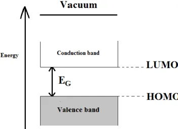
There are analogies between the electronic structure of organic and inorganic semiconductors. The highest occupied molecular orbital (HOMO) and the lowest unoccupied molecular orbital (LUMO) energy levels of organic semiconductors can be considered as the valence band edge and the conduction band edge of the semiconductor, respectively [17]. The energy difference between the HOMO and the LUMO is the band gap energy (EG) (Figure 1.3). Typical band gaps
for organic semiconductors are between 1.5 and 3 eV.
The conjugation, typical of organic semiconductors, causes the delocalization of the π electron of the sp2-hybridized C atoms. In turn, the delocalization enables charge carrier transport within the organic semiconductor.
There are two main possible charge transport mechanisms in organic semiconductors, namely hopping and band-like [13]. In polycrystalline organic semiconductors, with a few exceptions, the mechanism of transport is based on thermally activated hopping of the charge carriers through a distribution of localized states. In these organic semiconductors charge carrier mobility typically increases with increasing temperature. On the other hand, in highly ordered molecular crystals (single crystals), transport is described by band-like mechanism. The charge carrier mobility of single crystals typically decreases with increasing temperature [15].
In principle, organic semiconductors can support either positive (holes) or negative (electrons) charge carriers as the majority carriers [16]. In some cases, transport of both charge carriers can be observed. In this latter case the organic semiconductors are known as ambipolar.
The majority of organic electronic devices are based on thin films. To obtain thin films, small molecules can be processed both via solution and vacuum-based deposition techniques whereas polymers can be exclusively processed from solution [18].
Film morphology and structure, determined by the film nucleation and growth, dramatically affect the film functional properties, in turn affecting device performance [19].
For vacuum-based techniques, a number of deposition parameters can be controlled, such as the rate of deposition and the substrate temperature. For solution-based techniques, the key parameters for the film formation process are the solvent volatility and the concentration of the organic semiconductor in solution. In addition, the wettability of the substrate used for film growth are crucial in establishing a certain structure and morphology [20].
In this project, we studied the organic semiconductors Titanyl-phthalocyanine (TiOPc), Poly-3 (hexylthiophene) (P3HT), and P3HT/ phenyl-C61-butyric acid methyl ester (PCBM) blends. The chemical structure of these organic semiconductors is shown in Figure 1.4.
Figure 1.4: Chemical structures of TiOPc, P3HT, and PCBM.
TiOPc is a small molecule belonging to the metal phthalocyanine (MPc) family. Because of their volatility and high thermal stability (up to 400 ˚C [21]), metal phthalocyanines can be deposited by thermal evaporation [22]. The HOMO and LUMO level of TiOPc are about -5.7 and -3.9 eV (with respect to the vacuum level) respectively [23].
Most TiOPc OTFTs exhibit p-type behaviour. However, an n-type behaviour was reported under ultra high vacuum [24]. Li et al. achieved the highest μh of 3.31 cm2/V∙s in TiOPc OTFTs using
SiO2 substrates treated with a self assembled monolayer of octadecylthrichlorosilane (OTS) [25].
P3HT, which belongs to the family of polythiophenes, is a p-type solution-processable polymeric semiconductor soluble in a number of common organic solvents [26–29]. The HOMO and LUMO values of P3HT reported in the literature are around -4.9 and -3 eV (with respect to vacuum level), respectively [30], [31]. For OTFTs based on this polymer, the highest reported hole mobility (µh) is about 0.1 cm2/V∙s [26], [32].
The degree of P3HT regioregularity, the molecular weight (Mw), and the deposition conditions
significantly affect the performance of P3HT OTFTs. Sirringhaus et al. found that upon deposition of P3HT on a flat substrate, ordered lamellar domains (fine sheets of material) were formed. The orientation of these domains is related to the degree of regioregularity, the molecular weight, and the deposition conditions [32].
PCBM, a fullerene derivative, is a solution processable n-type small molecule [33]. The LUMO level of PCBM is located at about -4.3 eV [34] and the HOMO level is at about -6 eV [35] (with respect to the vacuum level).
1.3 Organic thin film transistors (OTFTs)
An OTFT is made of a thin film of organic semiconductor in contact with source (S) and drain (D) electrodes separated from the gate (G) electrode by a gate dielectric layer [36] (Figure 1.5). The region of the organic semiconductor delimited by the S and D electrodes is the transistor channel. The characteristic dimensions of a transistor are the inter-electrode distance (L) and the electrode width (W).
Figure 1.5: Schematic device structure of an OTFT. L and W are the length (L) and width (W) of the transistor channel.
The working principle of an OTFT can be described as follows: upon application of a gate voltage (VG), a thin sheet of mobile charge carriers is formed in the organic semiconductor. After
injection from the S and D electrodes, the charge carriers move within the transistor channel as a function of the applied drain-source voltage (VD). The source-drain current (ID) is modulated by
VG [13].
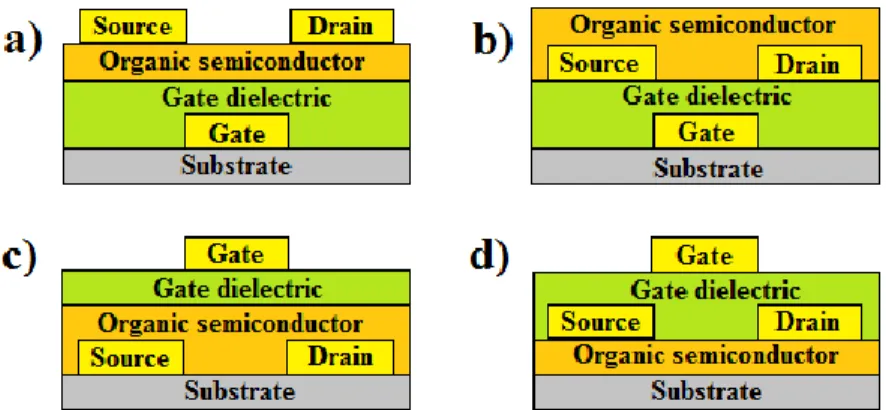
There are different possible architectures for OTFTs. The G electrode can be positioned either on top (top-gate) of the organic semiconductor or underneath it (bottom-gate). For each of these two cases, there are two different configurations of the S and D electrodes (bottom and top-contacts). Hence, four distinct OTFT architectures are possible, as illustrated in Figure 1.6. It should be noted that the specific architecture of electrodes affects the performance of OTFTs [13]. For example, different morphologies of the top and bottom surfaces of the organic semiconductor thin films [37] and the presence of trap states during electrode deposition on organic semiconductors for top-contact OTFTs [38], [39] can change the performance.
Figure 1.6: Four different OTFT architectures. (a) gate top-contact OTFT (b) Bottom-gate bottom-contact OTFT (c) Top-Bottom-gate bottom-contact OTFT (d) Top-Bottom-gate top-contact OTFT.
The main figures of merit of an OTFT are the charge carrier mobility (μ), the ON/OFF current ratio (ION/IOFF), the threshold voltage (VTH), the onset voltage (VON) and the subthreshold swing
(SS) [16]. The mobility [cm2/V∙s] is the velocity of the charge carriers per unit of applied electric field. ION/IOFF designates the switching performance of the device. It is defined as the ratio of
source-drain current (ID) in the ON and OFF states. The ON and OFF states are usually taken
where ID attains its maximum and minimum values, respectively, on the ID versus VG plot
(typically reported on a logarithmic scale), recorded at a certain VD. VON is the VG at which ID
abruptly increases.VTH indicates the minimum VG required to attain a quadratic dependence of ID
on VG (in the saturation regime, where the channel is pinched off) or the minimum VG required to
attain a linear dependence of ID on VG (in the linear regime, where the ID increases linearly with
VD). The SS is defined as dVG/dlog10ID in the subthreshold region, where VG is lower than VTH.
The intense research activity carried out in the last twenty years on organic semiconductor synthesis and OTFT engineering has led to significant improvements of the performance of OTFTs [36], [40].
The performance of OTFTs is affected by a complex interplay of factors, among which are the morphology and structure of the organic film [19] and the quality of the dielectric/organic film [36] and metal electrode/organic film interfaces [41].
The metal electrode/organic semiconductor interface plays a crucial role in establishing the performance of OTFTs, since charge carriers need to be injected from S and D electrodes into the
organic semiconductor before being transported within the transistor channel [42]. The presence of charge injection barriers at the metal electrode/organic semiconductor interface can lead to poor injection efficiency of OTFTs. In this context, the main purpose of this MSc work is to give a contribution to improve the efficiency of the injection of electrons and holes in OTFTs.
1.4 Charge carrier injection in OTFTs
In this section we briefly recall a few fundamental concepts about charge injection in OTFTs. The metal workfunction (Φm) is defined as the energy required to remove an electron from the
Fermi level of the metal to the vacuum. The ionization potential (IP) and electron affinity (EA) of an organic semiconductor are respectively the energy required to remove an electron from the HOMO level of the molecule to the vacuum, and the energy required to add an electron to the molecule (in the LUMO level) [43].
Because of the offset between the LUMO and HOMO levels of the organic semiconductor and the Fermi level of the metal, an energy barrier for charge carrier injection, the Schottky barrier, is present at the metal/organic interface [44],[45],[46]. It is possible to estimate the electron and hole injection barriers from the difference between the LUMO and HOMO levels of the organic semiconductor and the Fermi level of the metal, respectively. Therefore, the hole injection barrier (ΦB,h) is defined as:
Equation 1-1
and the electron injection barrier (ΦB,e) is defined as:
Equation 1-2
There are different charge carrier injection mechanisms possible for OTFTs (Figure 1.7) [42]. We will briefly illustrate them in what follows.
Figure 1.7: Different charge carrier injection mechanisms at a biased metal/organic semiconductor interface, in OTFTs. EV: Vacuum level, EF: Fermi level of the metal: (a)
Thermionic emission, (b) Field emission (tunneling), (c) Defect-assisted injection.
In Richardson-Schottky injection or thermionic emission, the charge carriers surmount the injection barriers upon application of an electrical bias if the thermal energy of charge carriers is greater than the charge carrier injection barrier. This model is valid at high temperatures or low injection barriers. The injected current density can be described as [47]:
π Φ Equation 1-3
where e is the elementary charge, m* the effective mass of the charge carrier in the semiconductor, V the voltage applied to the semiconductor, kB the Boltzmann constant, h the
Planck constant, T the temperature, and ΦB is the charge carrier injection barrier in the absence of
electric field.
In Fowler-Nordheim tunneling (field emission) mechanism, charge carriers tunnel through a thin energy barrier. This mechanism is found in the case of high injection barriers and it is enabled by high electric fields. The injected current density can be described as [48]:
Equation 1-4
where E is the electric field at the interface (the meaning of the other symbols is the same as for the previous equation).
In the defect-assisted injection, charge carriers circumvent the barrier by hopping through midgap states.
In general, OTFTs show low injection efficiency [49], [50] due to the presence of Schottky barriers [36]. This is different from what is observed in Si MOSFET technology, where implantation of atoms forming n-regions and p-regions at the contacts prevents the formation of injection barriers. The low injection efficiency in OTFTs leads to a sigmoidal shape of the current-voltage output TFT curves. On the other hand, the linear behavior of current-voltage output TFT curves indicates an ohmic behavior of the contacts, and consequently high injection efficiency. Injection efficiency can be defined as the ratio of the injection-limited current density (JINJ) versus the bulk-limited current density (JBULK) [41].
If we assume that we have a trap-free semiconductor and we neglect the diffusion of the charge carriers, at low voltages the current density flowing in the transistor channel is described by the Ohm law such that [41].
Equation 1-5
where N0 is the number of electrons per unit volume, V is the applied voltage, μ is the charge
carrier mobility, and L is the length of transistor channel.
An ohmic contact is defined as a contact where the injection efficiency (JINJ/JBULK) is one. Only if
the Fermi level of the metal is aligned to the LUMO or HOMO levels of organic semiconductor, an ohmic contact can be expected [41], [51], [52].
Other factors including the morphology and structure of the semiconductor at the metal/organic semiconductor interface can also dramatically affect the injection process. Interfacial charge carrier traps, dipoles (charge rearrangements upon interface formation) and chemical impurities, affecting the interfacial electronic structure, can also affect charge injection [52], [51]. Moreover, the presence of surface states (electronic states at the surface of materials where dangling bonds can be present) at the metal/organic semiconductor interface can produce a Fermi level pinning (a phenomenon where surface states stabilize the Fermi level of the semiconductor) making the estimation of Schottky barrier difficult [43].
using self assembled monolayer (SAM) to modify the metal surface, prior to organic semiconductor deposition [55]. Each one of these approaches presents major limitations. Low workfunction metals suitable for e- injection, such as Ca, are highly reactive in ambient conditions. Doping of organic semiconductors employed in OLEDs actually improved their performance but has to be selectively carried out in the vicinity of the contacts [54].
Blending of salts with organic semiconducting polymers has been investigated since almost twenty years in light emitting electrochemical cells, but can only be applied in solution processed organic semiconductors [56]. Moreover, this solution is not a viable one for OTFTs since it leads to a dramatic increase of the device OFF current and switch on times.
Modification of Au workfunction with SAMs of polar thiols such as perfluorodecanethiol on the metal surfaces prior to deposition of the organic semiconductor also leads to improved charge carrier injection [55]. However this approach is limited to Au electrode surfaces, where thiols can self-assemble [57–61].
There is then a need to explore novel approaches of general validity to improve charge carrier injection efficiency in organic semiconductor thin films of interest for OTFT applications. In this context, we propose in this MSc work the use of SWCNT array electrodes.
1.5 Charge carrier injection from CNT electrodes to organic
semiconductor thin films
Carbon nanotubes (CNTs) are being investigated by several research groups as electrode materials in organic electronic devices to improve the device performance [62–71].
Before presenting a literature review on CNTs used as electrode materials in organic electronics, we would like to briefly recall in this section a few fundamental properties of CNTs.
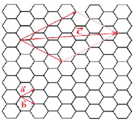
CNTs can be either single-walled (SWCNTs) or multi-walled (MWCNTs). A graphene sheet rolled up into a cylinder can form a SWCNT. MWCNTs consist of a series of coaxial SWCNTs. The circumference of a SWCNT is defined by means of the chiral vector where and are the unit vectors of the graphene sheet and n and m, the integer coefficients of the linear combination, are the chirality indices (Figure 1.8). A particular SWCNT is defined by n and m, usually denoted by (n, m) [72]. The electronic properties of CNTs depend on (n, m): if n-m=3j, where j is an integer, CNTs are metallic; otherwise, they are semiconducting [73].
Figure 1.8: A graphene sheet with unit vectors indicated by and . The vector defines the circumference of the CNT.
CNTs can be considered as quasi one-dimensional (1D) nanostructures due to the high aspect ratio of length-to-diameter (typically they are several μm-long and have a diameter of 1-2 nm [74]).
CNTs have remarkable properties such as high electrical conductivity (about 106-107 S/m [75]), high thermal conductivity (up to 3500 W/m∙K at room temperature [76]), chemical stability, and ease of processing [62], [77],[63].
We would like to mention some relevant examples of different applications of CNT electrodes in organic electronics in what follows.
transparent and conductive SWCNT sheets as anodes were achieved by Aguirre et al. [79]. They achieved a brightness of, 2800 cd/m2 a luminance efficiency, of 1.4 cd/A, a value to be compared with 1.9 cd/A observed using as the anode a conventional indium tin oxide (ITO) electrode. The comparable efficiency together with the flexibility of CNTs, to be compared to brittle ITO, make CNT films potential candidates to replace ITO electrodes in OLEDs.
Solution processed sensitive photodetectors, active in the visible portion of the electromagnetic spectrum, operating at room temperature, were fabricated using copper phthalocyanine (CuPc) in the form of Langmuir Blodgett monolayers as the photosensitive material and SWCNTs as the point contacts [71]. The fabrication of the point contacts was carried out by the initial fabrication of SWCNT transistor structures followed by the definition of a 5 nm gap within the tube by e-beam lithography and oxygen plasma etching [80]. The mobility in linear regime for the CuPc trasnsistor/photodetector was 0.4 cm2/V∙s which is the highest among those obtained from organic ultrathin film transistors. ION/IOFF of 104 and SS of about 450 mV/ decade were
calculated. These photodetectors exhibited responsivities greater than 108A/W.
A few studies have addressed the use of CNTs as electrodes in OTFTs which are presented here. Field-effect operation in organic transistors based on pentacene nanocrystals and metallic MWCNT S/D electrodes was reported [81]. The fabrication of the electrodes was such that initially MWCNTs, with diameter of about 10 nm and length of 5 μm, were synthesized by the arc-discharging method. Afterwards, two pads of Pt (10nm)/Au (40 nm) were defined on top of one MWCNT using electron-beam lithography, at a distance of 4 μm. The application of a high current (about 200 μA) at room temperature, in air, opened a gap shorter than 50 nm on the MWCNT [82]. Afterwards, pentacene was selectively grown on the electrode gap by vacuum sublimation through a poly (methylmethacrylate) (PMMA) 10 μm2 window, defined by electron beam lithography.
It was also shown in [83] that metallic SWCNTs can be used as quasi-1D electrodes to build organic field effect transistors (OFETs) with molecular-scale width (~2 nm) and channel length (down to 1-3 nm). Pentacene (vapor deposited) and P3HT (solution processed) were used as the organic semiconductors. For comparison with SWCNT-contacted devices, short channel OFETs with conventional metal electrodes were also fabricated (Pd, with Ti adhesion layer). At VD ≈ 0.3
V, the SWCNT-contacted FET exhibited a SS of about 400 mV/decade, while SS was about 4 V/decade for the metal-contacted FET.
Cao et al. fabricated mechanically flexible OTFTs based on ultrathin films of pentacene and transparent electrodes of SWCNTs networks, formed by transfer printing of pristine CNTs grown by chemical vapor deposition (CVD) [84]. The SWCNT networks were used for all the three electrodes in the OTFTs (G, S, and D electrodes). Mobility values as high as 0.5 cm2 /V∙s and ION/IOFF larger than 105 were observed. Cao et al. also fabricated analogous devices using Au
electrodes. The contact resistance (Rc) was significantly lower in SWCNT devices (Rc ~ 2×10⁵
Ω∙cm) compared to Au devices (Rc ~ 14×105 Ω∙cm). The behavior of the SWCNT electrodes was
ascribed to field focusing due to the high aspect ratio of the SWCNTs.
Decreasing of contact resistance in OTFTs based on pentacene by means of MWCNT electrodes was also reported in [85]. In this study, MWCNTs (with two different lengths: 400 nm and 1 μm) were deposited by thermal CVD, directly on the Fe/Ti S/D patterned electrodes playing a catalytic action towards the growth of the CNTs. The Fe/Ti catalytic layer was deposited through electron beam thermal evaporation and patterned using photolithography and lift-off. The lowest value of Rc ~ 3×10⁴ Ω∙cm were measured, together with μ of 0.14 cm2/V∙s and ION/IOFF > 106.
Liu et al. proposed a new architecture of application for CNTs [86]. They fabricated vertical OTFTs and vertical organic light emitting transistors (OLETs) using a network of SWCNTs as S electrode. Their architecture paved the way for the use of low mobility organic semiconductors and provided sub-μm channel lengths without need of high-resolution patterning. The fabrication of vertical OTFTs starts with transfer of SWCNT networks on a 200 nm thermal SiO2 heavily
p-doped silicon substrate, which provided the bottom G. Afterwards, the active layer poly[(9,9-dioctyl-fluorenyl-2,7-diyl)-alt-co-(9-hexyl-3,6-carbazole)] (PF-9HK) or N,N’-di(1-naphthyl)-N,N’-diphenyl-1,1’-diphenyl-1,4’-diamine (NPD) was deposited over the entire substrate on top
photoactive layer were deposited over the SWCNT network. The D electrode on top of the active layers was thermally evaporated LiF/Al. At a VD of -30 V, the luminance (green color) was 540
cd/m2, at a current density of 17.3 mA/cm2, for a reasonable efficiency of 3.1 cd/A, which is comparable to typical indium tin oxide anode, NPD/Alq3-based devices.
Southard et al. demonstrated pentacene and poly-3-hexylthiophene (P3HT) TFTs making use of transparent films of commercially-available SWCNTs produced by airbrushing from aqueous solutions as the S/D electrodes [87]. They obtained the μ of 0.093 cm2/V∙s and ION/IOFF > 106 (VD
= -60 V, -60 V ≤ VG ≤ 60 V) for pentacene TFTs and the μ of 0.014 cm2/V∙s and ION/IOFF > 105
(VD = -60 V, -60 V ≤ VG ≤ 50 V) for P3HT TFTs.
OTFTs using SWCNTs arrays as the S/D electrodes, kept on the substrates by Ti pads, and pentacene as the semiconductor were reported in [70]. In the same study, OTFTs analogues, making use of Au electrodes and Ti pads, were also prepared. OTFTs based on CNT array electrodes showed output characteristics indicating efficient injection. Pentacene showed an effective linear mobility of 0.14, 0.09, and 0.001 cm2/V∙s for CNTs array-, Au-, and Ti-based electrode devices, respectively.
McCarthy et al. fabricated a vertical OFET using a network of SWCNTs as the S electrode and dinaphtho-[2,3-b:2′,3′-f]thieno[3,2-b]thiophene (DNTT) as the organic semiconductor [88]. DNTT was deposited by vacuum sublimation on a CNT network spread on the gate dielectric. Finally DNTT was covered by an Au top D electrode. The figures of merit for the device were ION/IOFF >105for a VG range of 4 V, with a current density output exceeding 50 mA/cm2. In
another study [89], the same group applied the same architecture using pentacene as the organic semiconductor. ION/IOFF of around 105 was obtained while the transistor current density was about
Liu et al., used the same architecture of vertical FETs based on SWCNT networks as the S electrode to build high-performance non-volatile memory elements [90]. The SWCNT random network S electrode facilitates charge injection into the charge storage layer, which is a thin film of crosslinking polymer layer, benzocyclobutene (BCB), on top of the gate dielectric (a 200 nm thick thermal SiO2). After deposition of BCB, poly
(9,9-dioctyl-fluorene-co-N-(4-butylphenyl)-diphenylamine) (TFB) was used as the charge transport material. Au top D electrode was evaporated onto the active layer.
The same research group, recently demonstrated a vertical OLET using a SWCNT network S electrode that operates at low voltage (VON ~ -2.5 V) with low parasitic power dissipation (6.2 %)
and the near-full aperture emission (~98%) in the three primary colors (red, blue, green) [91]. The vertical OLET can be described as an OLED inserted into a vertical OTFT making use of CNT S electrode. Transparent indium tin oxide glass was used as a bottom G electrode on top of which the gate dielectric Al2O3 and a thin hydrophobic layer of BCB were sequentially deposited.
A diluted network of SWCNTs, optically and electrically transparent, was spread over the gate dielectric (made hydrophobic by the BCB layer) and served as the S electrode. The organic semiconductor DNTT was vacuum sublimed over the SWCNT network. Prior to deposition of the D electrode, the insertion of the OLED layers was done (on top of organic semiconductor). For emission of different colors, different emitter layers were used based on different iridium complexes.
Gwinner et al. demonstrated that the presence of small amounts of semiconducting SWCNTs dispersed in poly(9,9-di-n-octylfluorene-alt-benzothiadiazole) (F8BT) and poly(9,9 dicotylfluorene) (F8) increases both hole and electron injection in top gate/bottom contact ambipolar light-emitting field-effect transistors (LEFETs) based on these conjugated polymers [92]. The VTH and VON for both holes and electrons were decreased with respect to devices
without CNTs. Ambipolar currents and maximum light emission intensities were 1-2 orders of magnitude higher than in devices without CNTs.
In recent studies, the performance of CNT array electrodes in PCBM and CuPc TFTs revealed their superiority compared to conventional Au electrodes [93], [94]. Specifically, the linear behavior in the ID-VD characteristics of PCBM OTFTs based on CNT array electrodes at low VD
OTFTs). The linear mobility (at VD = 2 V) of CNT OTFTs was about two orders of magnitude
larger than linear mobility of Au OTFTs (μ ~1×10⁻² cm2/V∙s for CNT OTFTs and μ ~1×10⁻⁴ cm2/V∙s for Au OTFTs at room temperature).
These results demonstrated a higher mobility of CNT OTFTs at low bias as well as a lower VTH
and a higher ION/IOFF (at VG= 20 V, VTH ~ 6 V, ION/IOFF = 106 for CNT OTFTs; VTH ~ 10 V,
ION/IOFF = 105 for Au OTFTs). After vacuum annealing at about 130 ˚C for 16 h, PCBM OTFT
with CNT electrodes showed an ambipolar behavior, with ohmic injection of electrons and holes. The mechanism behind this change from unipolar to ambipolar is still under investigation. A similar conversion of unipolar to ambipolar transport had been previously shown in transistors using CNT as semiconductors where was attributed to the desorption of O2 and H2O molecules
from the surface of the SiO2 [95].
In OTFTs with CNT array electrodes based on CuPc thin films (deposited by supersonic molecular beam epitaxy, SuMBE), an ohmic hole injection was obtained [94]. In CNT devices, high μ of 1.2×10⁻²
cm2/V∙s at VG= -20 V and ION/IOFF of about 106 at VD= -1 V and VG= -10 V
were achieved while a μ of 5×10⁻³
cm2/V∙s and ION/IOFF of 103 were obtained for similar devices
using Au electrodes in the same conditions. Conversion of p-type to ambipolar OTFTs by vacuum annealing was also achieved.
High performance short channel pentacene OTFTs using aligned arrays SWCNT S/D electrodes was demonstrated by Sarker and co-workers. The mobility of 0.65 cm2/V∙s and ION/IOFF of
1.7 × 10⁶
were achieved, higher than those observed in other short channel devices [96].
To deeply understand the charge injection mechanism from CNT electrodes to organic semiconductors, a detailed knowledge of the CNT/organic semiconductor interface is required. However this interface has not been carefully characterized yet. The hypothesis to explain the
improvement of charge carrier injection in OTFTs using CNT electrodes is that, because of 1D structure of CNTs, the electric field at CNT/organic semiconductor interface is considerably enhanced in comparison with the interface between a metal electrode/organic semiconductor. This enhancement can originate sharper band bending in the CNTs/organic semiconductor interface and consequently improve charge injection.
It is worth noting that in transistors using semiconducting CNTs as semiconductor and Ti electrodes, the enhancement of electric field at the CNT/metal interface due to 1D structure was clearly identified [97], [98]. It was also mentioned that this enhancement can produce sharp band bending at the interface and consequently promote tunneling across the Schottky barrier.
A further hypothesis for improvement of charge injection in OTFTs based on CNT electrodes is that because of the conjugated structure of both CNTs and organic semiconductors, the CNTs can provide better contacts for organic semiconductors compared to metal electrodes.
1.6 Objectives of this work
The long-term objective of this work is to exploit SWCNT array electrodes to improve the charge injection in bottom-gate bottom-contact OTFTs [99], [100].
The approach is comparative i.e. it consists in comparing conventional metal electrodes (Au) and
novel SWCNT array electrodes. The hypotheses underlying the adopted approach are the
following:
The 1D structure of CNTs facilitate charge carrier injection by field emission;
The conjugated structure that CNTs and organic semiconductors have in common provides a favorable electrode/organic semiconductor interface, with low density of charge carrier traps.
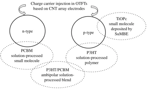
SWCNT array electrodes have been already successfully applied to pentacene, PCBM, and CuPc TFTs [70], [93], [94].
processable P3HT polymer and P3HT/PCBM blends, and, the vacuum processable (supersonic molecular beam epitaxy [SuMBE]) Titanyl-phthalocyanine (TiOPc) molecule. These organic semiconductors were selected to confirm and extend the results previously observed [70], [93], [94] (Figure 1.9). n-type p-type PCBM solution-processed small molecule P3HT solution-processed polymer TiOPc small molecule deposited by SuMBE P3HT/PCBM ambipolar solution-processed blend
Charge carrier injection in OTFTs based on CNT array electrodes
Figure 1.9: Scheme of the different organic semiconductors considered in this MSc work to investigate the behavior of SWCNT array electrodes in OTFTs.
We investigated vacuum deposited films of an organic semiconductor belonging to the metal phthalocyanine family, TiOPc, to extend the results previously observed with CuPc (p-type) [94]. Specifically, TiOPc films were deposited using the SuMBE technique.
P3HT was selected since this is a well-investigated polymer semiconductor, considered as a model polymer for fundamental studies in organic electronics. To date there are no studies related to the combination of organic semiconducting polymers and SWCNT array electrodes in OTFTs. P3HT/PCBM blends are an important example of bulk-heterojunction systems [101], i.e. systems where two (p- and n-type) organic semiconductors are mixed at the molecular/nanometric level. P3HT/PCBM ambipolar blends represent an interesting case of study since they enable the investigation of both electron and hole charge injection and transport in the same TFT. The study of blends opens the possibility to use CNT array electrodes in ambipolar devices such as OLETs.
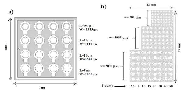
concentric electrode geometry is the most suitable to evaluate the performance of common gate OTFTs, since it permits to circumvent parasitic currents [102]. The device structure used in this project is illustrated in Figure 2.1.
Figure 2.1: Structure of bottom-gate bottom-contact OTFTs used in this work: top view (a) and cross section (b). Doped Si served as substrate and G electrode.
The employed substrates were highly doped (n-type) Si (100) wafers (resistivity of 0.002-0.003 Ω∙cm) covered with either 100 nm or 200 nm-thick thermally grown SiO2 dielectric (100 nm:
34.5 nF/cm2 capacitance, 200 nm: 17.26 nF/cm2 capacitance), where Si acted as substrate and G electrode in OTFTs.
The first step to fabricate SWCNT array electrodes was vacuum filtration of the SWCNT solution using cellulose filters [103]. For this purpose, 2% sodium cholate aqueous dispersion of SWCNTs (1×10⁻⁴ mg/mL), a vacuum filtration apparatus, and a Millipore membrane filter with pore size of 0.22 μm were used. The vacuum filtration apparatus (Figure 2.2) includes a funnel that hosts the cellulose filters, a flask, and tubing connected to house vacuum (about 1 mTorr).
Figure 2.2: Vacuum filtration apparatus used in this work.
Typically, 4 mL of SWCNTs sodium cholate solution were diluted in 50 mL water. The density of the SWCNT network deposited on SiO2 depends on the concentration of the SWCNT solution.
Before filtering the SWCNT solution, the filter was wet with 50 mL of water to ensure adhesion of filter on funnel. The addition of SWCNT solution started when a small amount of water was still present in the funnel. After filtration, the cellulose filter containing the SWCNTs was dried for one day in ambient conditions.
The SiO2/n-Si substrates were cut into small pieces (2 cm × 2 cm) and cleaned by sonication
(using an Eumax ultrasonic cleaner UD100SH-4L) in isopropyl alcohol (IPA), acetone and again IPA for 5 mins, 10 mins, and 5 mins, respectively (IPA and acetone were obtained from J.T.Baker company). The SiO2 surface was then treated with 1,1,1,3,3,3-hexamethyldisilazane
(HMDS, Gelest, 99%) to improve adhesion of SWCNTs. HMDS was applied by spin coating (1000 rpm, for 1 min). Deposition of SWCNT networks on the SiO2 surface of the substrates was
achieved with the following procedure:
1. To transfer the SWCNTs from the cellulose filters to the SiO2 surface, the filters were
dipped in 1, 2-dichlorobenzene (DCB) for about 1 min.
2. The filter containing SWCNTs was placed on the SiO2 surface treated with HMDS.
3. The substrate was gently rinsed with acetone to dissolve the cellulose filter.
4. When the filter on the substrate started to dissolve, the substrate was transferred into a beaker containing acetone for about 30 mins.
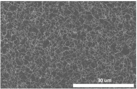
The SWCNT networks were then inspected with a field emission scanning electron microscopy (FE-SEM, Hitachi S-4700). The SEM images were acquired in the secondary electron imaging mode using the upper detector (Everhart-Thornley detector), at 1 keV accelerating voltage, and 1 µA emission current and 5 mm working distance. SWCNTs appear bright on an insulating substrate, when imaged under low accelerating voltage operation (Figure 2.3) [104].
Figure 2.3: SEM image (1 keV, 7 µA) of a SWCNT network deposited on SiO2.
The patterning of S and D electrodes was achieved by photolithography and lift-off in the LMF clean room (class 1000). The SWCNT-coated substrates were first kept on a hot plate at 190 ˚C for about 20 mins to remove adsorbed water. Then, the lift-off resist LOR 1A (Microchem) was spun onto the SWCNT-coated substrate at 2000 rpm for 1 min. After soft baking (at 190 ˚C for 3 mins), the positive tone photoresist S1805 (Shipley) was spun on LOR 1A and baked at 115 ˚C for 1 min. The sample was then exposed to UV light through a photo mask in a Karl Suss mask
aligner (MA-4). Hard contact in constant power mode was used for exposure. Two different photo masks were used to pattern concentric S and D electrodes with different W and L values (Figure 2.4).
Figure 2.4: Two different photo masks for patterning circular S and D electrodes, used in this work. Each photo mask consists of several patterns of either (a) or (b).
The photoresist was then developed in MF319 (Microchem) developer for 75 seconds. The exposed regions of S1805 photoresist were dissolved in the developer leading at the same time to dissolution of the underlying LOR 1A layer from the opened windows. This procedure reproduces the patterns of the photo mask on photoresist. Finally, the photoresist-SWCNT-coated substrate was immersed in a beaker containing deionized water for 1 min, rinsed several times with deionized water in order to completely remove the residual developer, and dried with the N2
jet.
Figure 2.5: SEM image (1 keV, 7 µA) of the photoresist-SWCNT-coated substrate, after patterning the photoresist.
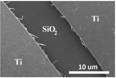
In order to make contact pads to SWCNT electrodes, a 20 nm-thick Ti film was deposited at a deposition rate of 0.1 nm/s using a Edwards Auto 306 electron beam evaporator in vacuum (10-6 -10-7 mbar) and patterned by a lift off process, which was achieved by immersing the sample in Remover PG (Microchem) at 70 ˚C for half an hour. This step was followed by rinsing the sample at room temperature with the remover PG and subsequently with IPA. Washing with deionized water and drying with N2 were the last steps of the lift-off procedure. During lift-off, a
Ti pattern, complementary to the photoresist pattern, was obtained (Figure 2.6).
The following step to complete the fabrication of SWCNT array electrodes was a sonication of the samples for a few minutes while immersed in AZ Stripper (AZ Electronic Materials). The sonication removes the SWCNTs not directly attached to the Ti pads and cuts the SWCNTs directly attached to the Ti pads such that only SWCNTs few hundreds of nanometers-long remain on the substrate. After sonication in AZ Stripper, the samples were immersed in IPA followed by washing in deionized water. The sonication time depends on the amount of SWCNT solution used in vacuum filtration; therefore it needs to be optimized for each sample. Figure 2.7 shows a SEM image of the sample with bright SWCNT arrays connected to metallic (Ti) pads.