HAL Id: cea-01659809
https://hal-cea.archives-ouvertes.fr/cea-01659809
Submitted on 17 Jan 2018
HAL is a multi-disciplinary open access
archive for the deposit and dissemination of
sci-entific research documents, whether they are
pub-lished or not. The documents may come from
teaching and research institutions in France or
abroad, or from public or private research centers.
L’archive ouverte pluridisciplinaire HAL, est
destinée au dépôt et à la diffusion de documents
scientifiques de niveau recherche, publiés ou non,
émanant des établissements d’enseignement et de
recherche français ou étrangers, des laboratoires
publics ou privés.
X-ray microscopic investigation of molecular orientation
in a hole carrier thin film for organic solar cells
Quentin Arnoux, Benjamin Watts, Sufal Swaraj, Francois Rochet, Ludovic
Tortech
To cite this version:
Quentin Arnoux, Benjamin Watts, Sufal Swaraj, Francois Rochet, Ludovic Tortech. X-ray microscopic
investigation of molecular orientation in a hole carrier thin film for organic solar cells. Nano Research,
Springer, 2017, 5, pp.2771-2782. �10.1007/s12274-017-1907-6�. �cea-01659809�
X-ray microscopic investigation of Molecular Orientation in a Hole Carrier Thin Film for Organic Solar cells
Quentin ARNOUX,1,2,3,* Benjamin WATTS,4 Sufal
SWARAJ,5 François ROCHET,1,5 Ludovic
TORTECH,2,3,*
1 UPMC, LCPMR, France. 2 UPMC, IPCM, France. 3 CEA Saclay, NIMBE, France. 4 Paul Scherrer Institute, Switzerland 5 Synchrotron SOLEIL, France.
12
In the present article, we investigate the morphology of an organic layer (2,2’,6,6’-tetraphenyl-4,4’-dipyranylidene, DIPO-Ph4) deposited under
vacuum on a silicon nitride (Si3N4) substrate. The films were
characterized by Atomic Force Microscopy (AFM) and Scanning Transmission X-Ray Microscopy (STXM) to gain an insight into the material growth.
Quentin ARNOUX, http://iramis.cea.fr/nimbe/Pisp/quentin.arnoux/ Ludovic TORTECH, http://www.ipcm.fr/TORTECH-Ludovic
X-ray microscopic investigation of Molecular Orientation in a
Hole Carrier Thin Film for Organic Solar cells
Quentin ARNOUX,1,2,3 () Benjamin WATTS,4 Sufal SWARAJ,5 François ROCHET,1,5 Ludovic TORTECH,2,3 ()
1 Sorbonne Universités, UPMC Univ Paris 06, UMR 7614, Laboratoire de Chimie Physique Matière et Rayonnement (LCPMR),
F-75005 Paris, France.
2 Sorbonne Universités, UPMC Univ Paris 06, UMR 8232, Institut Parisien de Chimie Moléculaire (IPCM), F-75005, Paris, France. 3 CEA Saclay, IRAMIS, NIMBE (UMR 3685), Laboratoire d'Innovation en Chimie des Surfaces et Nanosciences (LICSEN), F-91191
Gif-sur-Yvette, France.
4 Paul Scherrer Institute, 5232 - Villigen Psi, Switzerland.
5 Synchrotron SOLEIL, L’Orme des Merisiers, Saint-Aubin, BP 48, F-91192 Gif-sur-Yvette, France.
Received: day month year / Revised: day month year / Accepted: day month year (automatically inserted by the publisher) © Tsinghua University Press and Springer-Verlag Berlin Heidelberg 2011
ABSTRACT
Because dipyranylidenes are excellent hole carriers, their application in organic solar cells or organic light emitting diode is envisaged. In the present article, we investigate the morphology of 2,2’,6,6’-tetraphenyl-4,4’-dipyranylidene (DIPO-Ph4) deposited under vacuum on a silicon nitride (Si3N4) substrate, a paradigmatic system
for the study of molecular crystal/inorganic substrate interfaces. Samples with various coating ratios and different thermal treatments were prepared. The films were characterized by Atomic Force Microscopy (AFM) and Scanning Transmission X-Ray Microscopy (STXM) to gain an insight into the material growth. Results show a change of orientation at a molecular level depending upon the evaporation conditions. We are now able to tailor organic layer with a specific molecular orientation and a specific electronic behavior.
KEYWORDS
Organic solar cells; Scanning Transmission X-ray Microscopy; Molecular orientation
Introduction
Organic electronic devices are becoming increasingly commercially viable due to their continuously improving efficiency in the recent years and the tremendous amount of research targeted in maintaining relatively high efficiencies along with their low cost of production and technological ease of transfer. [1,2] The recently recorded high efficiencies of these devices [3–7] are still well below the
theoretical maximum efficiencies. [8] It is now well known that to improve the performance of these devices it is imperative to have a thorough understanding and complete control on the various aspects of the complex morphological architecture of these devices. Generally, these electronic devices are fabricated in a stack-like geometry of 𝑝-type and 𝑛-type semiconductors, either in the form of bilayers or blends sandwiched between charge transporting electrodes. These electrodes are primarily a Nano Res
DOI (automatically inserted by the publisher)
transparent indium tin oxide (ITO) film that acts as a hole collector and an evaporated aluminum metal that acts as an electron collector. To improve the durability and the efficiency of the organic photovoltaics (OPV), interfacial layers (IFLs) are used to bridge the electronic and morphological gap between the electrode and the active layer. The IFL at the anode is made of organic materials (polymers, small molecules), of graphene oxide [9] or even of inorganic material like NiO. [10] It is systematically deposited between the indium tin oxide (ITO) electrode and the standard photovoltaic active layers (often a P3HT:PCBM blend). [11] The most widely used IFL is the PEDOT:PSS polymer because of its high conductivity and easy processability, but its high acidity can lead to ITO deterioration. [11] To circumvent this difficulty some of the present authors have explored the benefit of depositing a 𝑝 -type molecular solid of the DIP family (2,2',6,6'-tetraphenyl-4,4'-dithiapyranylidene, DIPS-Ph4) on
ITO to finally form an ITO/DIPS-Ph4/P3HT:PCBM/LiF/Al cell in which the short-circuit
density ( 𝐽𝑆𝐶 ) [12] is efficiently increased. Current
sensing contact mode atomic force microscopy (CS-AFM) shows that there is a considerable increase in the total number of hole-carrying pathways with respect to a PEDOT:PSS IFL. [12]
Besides the favorable alignment of energy levels of the molecular solid with the ITO band structure, the increase in the hole-collection efficiency is also related to the interfacial morphological aspects. Charge conduction goes through molecular orbitals (MOs), more particularly through highest occupied molecular orbital (HOMO) for hole transport and lowest unoccupied molecular orbital (LUMO) for electron transport. With flat conjugated molecules, this implies that charge conduction goes through 𝜋 MOs which are perpendicular to the mean molecular plane. Thus, from one molecule to another, the charge transfer will be enhanced with molecules packed plane-to-plane and laid flat to the surface. Therefore, the charge transport is strongly linked to the
molecular orientation: angle between the molecules and their respective angles with the substrate. In this context, it is important to stress upon the significance of an adapted characterization tool, such as scanning transmission x-ray microscopy (STXM) that has the potential to disentangle molecular domain orientation information in thin films. [13] STXM, and other synchrotron based soft X-ray characterization tools such as resonant soft X-ray scattering, are already been widely used in conjunction with other laboratory based techniques to investigate the complex morphology of OPVs. [14–20]
Figure 1. (a) DFT geometric optimization of the free DIPO-Ph4
molecule (dark, white and red spheres correspond to C, H, and O atoms respectively); (b) Molecular orientation inside the molecular solid according to Chasseau et al.. [21]
The present study examines the growth of a molecular solid 2,2’,6,6’-tetraphenyl-4,4’-dipyranylidene (DIPO-Ph4, Figure 1) on Si3N4 substrates. DIPO-Ph4 is a
promising molecule to create an effective hole-conducting IFL at the transparent anode in OPV. [22] It forms a high-conductivity donor-acceptor complex with tetracyanoquinodimethane (TCNQ). [23] Its oxidation potential of 0.24 V (relative to ferrocene) makes it a better electron donor than tetrathiafulvalene (TTF). Its ionization energy is ~ 4.6 eV, according to Forrest’s relationship. [24] The geometry of the free molecule is depicted in Figure 1(a): the four phenyls are almost parallel to the dipyranylidene core, the dihedral angle being ~ 18°. [25] In the solid state, molecules pack plane-to-plane in columns and the dihedral angle of the phenyl groups reduces to 7.6 – 10.2° (Figure 1(b)). [21] DIPO-Ph4 is deposited on commercial Si3N4 substrates
evaporation. Changes in the morphology of the deposits with thermal treatment are monitored (ex
situ) by atomic force microscopy (AFM). STXM is then
carried out to obtain orientation sensitive information in the bulk of the deposits at a relatively high spatial resolution. Complementary density functional theory (DFT) calculations of the HOMO and LUMOs are performed to estimate the electronic transitions. We performed the measurements for 3 samples prepared under different evaporation conditions. The objective was to obtain a class of reference samples presenting different molecular orientation.
1 Experimental
1.1 Synthesis and chemical characterization
DIPO-Ph4 (see Figure 1(a)) has been prepared
following a synthesis the CEA team developed. [26] The final compound was characterized via Nuclear Magnetic Resonance (NMR) and via elementary analysis (see Table S1). No contamination was detected. Chasseau et al. [21] has described the crystallization structure via X-ray diffraction (XRD) investigations. In molecular solids, molecules are V-shaped such as presented in Figure 1(b).
1.2 Sample preparation
All DIPO-Ph4 deposits were prepared on commercial
Si3N4 substrates of thickness of 100 nm. After
introduction into a high vacuum ( ~ 10−6 mbar)
evaporation chamber, the Si3N4 substrate was exposed
to a molecular beam of DIPO-Ph4 using a Knudsen cell
positioned at 30 cm from it. The direction of the molecular beam was positioned at normal angles with the surface plane. A quartz balance (QB) monitor allows us to follow the deposition rate. DIPO-Ph4 is
evaporated at a speed of 1 Å· min−1 and the layer is
finally characterized by the average number of molecules per cm2 (QB-coverage).
Two identical samples were prepared while keeping the substrate at room temperature and with a QB-coverage of 1×10¹⁵ molecule·cm−2 evaporated (Sample
A & B). One of these samples (Sample B) was post-annealed at 𝑇 ≥ 170 °C and at atmospheric pressure for 1h. The objectives were to perform molecular desorption and to have access to the first layers
deposited. A third sample (Sample C) was prepared on a hot substrate 𝑇 ~ 100 °C during the evaporation of 10×1015 molecule·cm−2.
1.3 Atomic force microscopy (AFM)
The surface morphology of the DIPO-Ph4 films was
investigated via Atomic Force Microscopy (AFM). The AFM used was a Molecular Imaging from Agilent, PicoLE, used in contact mode using a Pt/Ir tip of radius 20 nm. The spring constant of the cantilever is 0.2 N·m−1. The vertical resolution in contact mode is
0.5 nm.
1.4 Density Theory Functional theory (DFT) calculations
We also performed Density Functional Theory (DFT) of the electronic structure of the isolated molecular (Kohn-Sham molecular orbital energies) of the molecule to substantiate the interpretation of our absorption results. We used the TURBOMOL package, adopting the B3-LYP functional and the def2-SV(P) base. The geometric optimization is given in Figure 1(a).
1.5 X-ray microscopy and data analysis
STXM has been performed on PolLux beamline (Switzerland Light Source). Samples were introduced in the analysis chamber which was then pumped down to ~ 10−3 mbar. The absorption stacks were
recorded at the C 1s edge (280 to 340 eV) with an X-ray beam normal to the surface and horizontally polarized. A zone plate with an outer ring spacing of 25 nm was used that allowed for a spatial resolution of ~ 30 nm. The image stacks were post processed using aXis2000. [27] The optical density (OD) was obtained using the 𝐼0 on the area between the
DIPO-Ph4 clusters (absorption of the Si3N4 substrate) and the
decomposition of the stacks into main spectral components was performed via Principal Component Analysis (PCA). For Sample B, we only measured spectra via a linescan to minimize X-ray dosage to the molecular clusters. Absorption spectra were normalized to the edge jump and were fitted using an error function curve as background, [28] centered at 288.9 eV. Energy calibration of the beamline was checked by measuring a reference PCBM (Phenyl-C61-butyric acid methyl ester) film. Main transitions have been fitted with Gaussian.
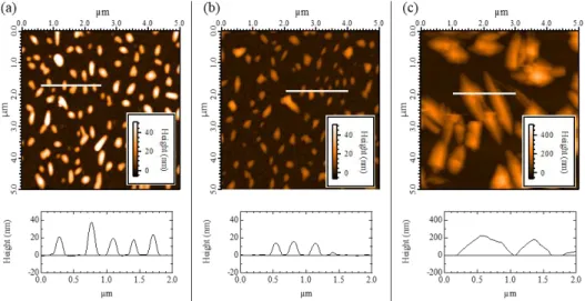
Figure 2. AFM images: (a) Sample A: No annealing treatment sample with QB-coverage of 1×10¹⁵ molecule·cm−2; (b) Sample B:
QB-coverage of 1× 10¹⁵ molecule· cm−2 with a post-annealing treatment at 𝑇 ≥ 170 °C; (c) Sample C: QB-coverage of 10 × 1015
molecule·cm−2 evaporated on a hot substrate (𝑇 ~ 100 °C).
2 Results and discussion
2.1 DIPO-Ph4 layer morphology studied via AFM
Atomic force microscopy (AFM) is used to examine the samples that were subsequently examined by absorption spectroscopy. As the morphological information of the deposited layer is detrimental to correctly interpret our absorption data, the AFM images (shown in Figure 2) are discussed first. To avoid any damage of the very thin window, the substrates are not cleaned before the evaporation. In that case, the silicon nitride has a native oxide layer at the surface. [29] The roughness of the Si3N4 substrate
(presented in Supporting information Figure S1) is 0.5 nm (root mean square, RMS). The DIPO-Ph4 coverage
is monitored during the evaporation in the evaporation chamber via a quartz balance (QB-coverage). The weight increases per surface unit during the evaporation. Finally, it is converted into a molecular surface density using the density given by Chasseau et al.. [21] After the deposition of 1× 10¹⁵
molecule·cm−2, the AFM image (Sample A, Figure 2(a))
shows that 3D elongated clusters (“mounds”) cover 25% of Si3N4 surface. The average height of the cluster
is 30 nm with an average diameter of 250 nm. Given the cluster density, an average volume of DIPO-Ph4
per surface unit is obtained, leading to a molecular surface density of 1.07×10¹⁵ molecule·cm−2 in excellent
agreement with the QB-coverage. After a post-annealing treatment at 𝑇 ≥ 170 °C (Sample B, Figure 2(b)). The average height of the cluster decreases to 13 nm. The mounds still cover 20% of the Si3N4 surface
with an average diameter of 230nm. The molecular surface density is divided by 3 (0.3 × 10¹⁵
molecule· cm−2). For the last sample (Sample C), 10
times more molecular material have been evaporated,
i.e. 10× 1015 molecule· cm−2 as QB-coverage, on a hot
substrate (𝑇 ~ 100 °C). The DIPO-Ph4 layer covers
now 60% of the Si3N4 surface. Clusters are no more
circular but look like large molecular crystals. The average height is 200 nm and the molecular surface density calculated from AFM image is 10.5 × 10¹⁵
molecule·cm−2 which is still in great agreement with
the QB coverage.
These observations are discussed below. When layers are deposited over homogeneous substrates, like single crystals, two main types of growth are classically considered, namely Volmer-Weber and Stranski-Krastanov growth. [30] In a Volmer-Weber growth, the organic molecules cluster in islands, leaving bare substrate areas. This arises from the fact that the interaction between molecules (𝜋-stacking) is much stronger than the interaction between the DIPO-Ph4 molecule and the Si3N4 substrate.
Alternately, in a Stranski-Krastanov growth, the molecule-molecule interaction competes with molecule-substrate interactions. A thin wetting layer covers all the substrate, on top of which the 3D island growth mode takes place. To calculate the molecular surface density, only the molecular clusters were taken in account. As the measurements are in good agreement with the QB-coverage, the wetting layer, if present, should not exceed ~ 2 nm. Concerning the
post-annealed sample, it was possible to decrease the average height of the clusters while keeping constant the overall area coverage and the average diameter of the cluster. With such a sample, it is possible to have access to the first layers evaporated which are representative of the initial stages of the evaporation in the first sample. As far as the 10×1015 molecule·cm−2
QB-coverage is concerned, there is a complete change in the layer morphology. The energy brought during the evaporation, on the hot substrate, changes the molecular growth by increasing the molecule diffusion on the surface.
2.2 Molecular description and electronics transitions
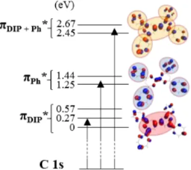
For STXM analysis, it is firstly important to have a good understanding on the electronic mechanism which will take place during the absorption process. DFT calculation was used to describe the empty molecular state (LUMO) centered on the C of DIPO-Ph4 (Figure 3). Furthermore, it was useful to visualize
the concerned molecular orbital (MO) to have information on the orientation. In fact, to determine the molecular orientation inside the clusters, we must be sure that there is an MO with one main direction.
Figure 3. Electronic scheme of the C 1s transition, indicated
energy are related to the LUMO and three OM are represented with an isovalue of 0.04 (LUMO, LUMO +3 and LUMO +5). The principal weight localization of the OM is emphasized with ellipse.
The lowest unoccupied molecular orbital (LUMO) and unoccupied MO of higher energy (LUMO+1 to LUMO+6) where described via DFT calculation. LUMOs are mainly composed of 𝜋∗ MOs which are
perpendicular to the dipyranylidene (DIP) core or to the phenyl (Ph) groups. They can be divided in 3 groups. A first one is centered at ~ 0.3 eV above the LUMO and composed of LUMO, LUMOs +1 and +2. The second one is centred at 1.3 eV above the LUMO and composed of LUMOs +3 and +4. The last one is centered at 2.3 eV above the LUMO and is composed of LUMOs +5 and +6. Looking to the localization of these groups, it appears that the first one is more localized on the DIP core, whereas the second one is more localized on the Ph groups. For the last one, the MOs are, with the same weight, on the DIP and on the Ph groups. These three groups will be now called 𝜋DIP∗ , 𝜋Ph∗ and 𝜋DIP+Ph∗ .
The geometry of the free molecule is depicted in Figure 1: the four phenyls are almost parallel to the DIP core, the dihedral angle being 18°. In the solid state, molecules pack plane-to-plane in columns and the dihedral angle of the phenyl groups reduces to 7.6 – 10.2°. Consequently, there is one main plane following the DIP core and four other planes following each of the four Ph groups. Thus, for the 𝜋DIP∗ MOs there is one main direction which is
perpendicular to the DIP core. As the contrary, for the 𝜋Ph∗ MOs, there is no main direction and finally, the
𝜋DIP+Ph∗ MOs have no main orientation because they
are localized both on the DIP core and on the Ph groups. The X-ray absorption results in the 𝑒− transition from core level to empty state. Thus, the absorption efficiency depends on the energy level of the empty states. It will also rely on the relative geometry between the electrical component of the X-ray beam and the direction of the MOs. Therefore, for DIPO-Ph4 molecule, absorption will be high if the
polarization is parallel to the 𝜋DIP∗ , so perpendicular
to the molecule. In other terms, with an X-ray beam normal to the surface (polarization parallel to the surface) there will be high absorption at 𝜋DIP∗ energy
if DIPO-Ph4 molecule are perpendicular to the surface
(𝜋DIP∗ parallel to the surface).
2.3 Scanning X-ray Microscopy
Figure 4. STXM images in thickness at photon energy 285 eV: (a) Sample A; (b) Sample B; (c) Sample C.
The STXM results have firstly been used to confirm the thickness of the layers and thus, compare with the AFM results. The obtained image at ℎ𝜈 = 285eV, corresponding to the maximum absorption at the C K edge (at 285 eV, Figure 4), is extracted from the image stack [𝑋; 𝑌; ℎ𝜈] to obtain the optical density ( 𝑂𝐷 ) images ( [𝑋; 𝑌] ) at 285 eV. This image is used to calculate the corresponding thickness using (1):
𝑂𝐷 = ln (𝐼0 𝐼)
𝑂𝐷 = 𝜇𝜌𝑙 (1)
where 𝜇 is the photoabsorption cross section, 𝜌 is the density and 𝑙 the thickness. We present the results in the same way as AFM images but in the images (Figure 4) are obtained from the absorption measurements.
For Sample A (1 × 10¹⁵ molecule · cm−2 QB-coverage
sample), the STXM image (Figure 4(a)) shows clusters with average height of 30 nm. This agrees with the AFM results. For the post-annealed sample (Sample B), STXM image (Figure 4(b)) is also in good agreement with an average cluster height of ~ 10 nm. We also have the same conclusion for the Sample C (10× 1015 molecule· cm−2 QB-coverage sample) where
the average cluster height is found to be 250 nm. The morphology is also confirmed for the different samples: circular cluster for Sample A and Sample B whereas there is large molecular crystal for Sample C. [𝑋; 𝑌] STXM analyses are in great agreement with AFM results.
Absorption spectra
Further investigation of the [𝑋; 𝑌; ℎ𝜈] stacks were performed with respect to the photon energy related variation (spectroscopy). Using PCA (Principal Component Analysis), we determined the main absorption spectra) of the stacks. Then, the first four components have been used to decompose the STXM stacks in four main regions. For each region, the absorption spectra are then extracted. These spectra are the average one for the defined region. After normalization, spectra have been fitted as described in the experimental part. The potential ionization (𝐼𝑃 at 288.9 eV) value was determined previously from the XPS C 1s binding energy and the measurement from the work function. Results for Sample A are presented in Figure 5.
Figure 5. Sample A: (a) STXM decomposition mapping; (b) Absorption spectra extracted for each region (the substrate (Sub) spectrum
is not represented as there is no absorption from this region); (c) 𝜋∗ area after substraction of the error function step function background
(at 𝐼𝑃) and the 𝜎∗ area
Table 1. Experimental 𝜋∗ transitions, FWHM of the Gaussian contribution and 𝜋∗/𝜎∗ ratio. For post-annealed sample, there were not
enough signal to determine 𝜋Ph∗ contribution.
Sample/Region Energy (eV) G-FWHM (eV) 𝝅
∗ /𝝈∗ (%) 𝝅𝐃𝐈𝐏∗ 𝝅𝐏𝐡∗ 𝝅𝐃𝐈𝐏+𝐏𝐡∗ 𝝅𝐃𝐈𝐏∗ 𝝅𝐏𝐡∗ 𝝅𝐃𝐈𝐏+𝐏𝐡∗ 𝝅𝐃𝐈𝐏∗ 𝝅𝐏𝐡∗ 𝝅𝐃𝐈𝐏+𝐏𝐡∗ 𝚺 Not-annealed Top 284.98 286.22 287.96 0.92 0.88 1.77 11 2 12 26 E2 285.00 286.23 287.98 0.92 0.81 1.76 10 2 13 24 E1 285.01 286.33 287.97 0.95 0.75 1.68 8 1 12 21 Post-annealed Top 294.94 _ 287.63 0.94 _ 1.95 6 _ 5 11 E 294.95 _ 287.58 0.93 _ 1.34 4 _ 3 7
The decomposition of the [𝑋; 𝑌; ℎ𝜈] stack for Sample A (Figure 5(a)) leads to four regions precisely localized on the sample. The main region is the one localized between the organic cluster. There is no absorption (or at least too low to be seen with the STXM thickness resolution). This is absorption from the substrate. The organic mounds are decomposed in three regions: one at the top and two on the edge. These regions will be now named Top, E2 and E1 respectively.
Absorption spectra have been extracted for these regions and edge-jump normalized for comparison (Figure 5(b)). A clear distinction of the 𝜋∗ and the 𝜎∗ regions is evident in the figure. After subtraction of the background and the 𝜎∗ region, the 𝜋∗ region is emphasized in Figure 5(c) for clarity. It has been fitted with three Gaussian curves (G-FWHM are indicated in Table 1). The first one centered at ~ 285 eV is attributed to the first transition group 𝜋DIP∗ . 𝜋Ph∗ is at
~ 286 eV and 𝜋DIP+Ph∗ centred at ~ 288 eV. DFT
calculation for a free molecule gives a 𝜋Ph∗ − 𝜋DIP∗ of
~ 1.3 eV and a 𝜋DIP+Ph∗ − 𝜋DIP∗ of ~ 2.3 eV (see
Figure 3). Experimentally, the value for the 𝜋Ph∗ −
𝜋DIP∗ is ~ 1.2 eV which is very close to the theoretical
calculation. For the 𝜋DIP+Ph∗ transition, the difference
with the 𝜋DIP∗ is ~ 3.1 eV. This value is 1 eV higher
than the theoretical one. The G-FWHM of the 𝜋DIP∗
transition is larger than of the 𝜋Ph∗ transition.
In the absorption spectra, we also focused on the contribution of the 𝜋∗ transition in comparison to the 𝜎∗ one. The intensity of the 𝜎∗ transition remain
identical between spectra extracted from Top to E1 regions. This was used as a reference to evaluate the 𝜋∗ transition in the different regions. The 𝜋∗/𝜎∗ ratio
decreases from Top to E1 (from 26% to 21%).This evolution is mainly due to a decrease of the 𝜋DIP∗
transition (from 11% to 8%). This transition is the only one which can be used for the molecular orientation. Thus, in the organic layer, there is an evolution in this orientation from the edge to the top of the cluster. In
the later regions, molecules are oriented perpendicularly to a higher degree than in the edge. This implies that there is a change in the orientation between the layer near the substrate and the top layers. The analysis of the post-annealed sample could allow us to extract information on the first layers evaporated. Unfortunately, the small amount of organic material in this sample makes the analysis harder due to a weak signal at normal X-ray incidence. To overcome the issue, we tilted the sample (30° between the normal and the sample surface). To decrease beam damage, we only performed a linescan along the organic cluster (Figure 6). We extracted from this line the edge (E) and Top spectra. The values of the 𝜋∗ transitions are given in Table 1. To make a comparison between the two samples, we performed tilted incidence angle experiments on Sample A. Results are presented in supporting information Figure S2, Figure S3 and Table S2. There were not changes from the previous analysis as we chose a small tilt angle: the 𝜋∗ interaction is more efficient than the 𝜎∗ one.
Figure 6. Sample B: (a) STXM image in thickness (at 285 eV)
with the position of the linescan (white dotted line); (b) Absorption spectra extracted for edge (E) and Top region (the substrate (Sub) spectrum is not represented as there is no absorption from this region).
For Sample B, 𝜎∗ transition is much higher than in Sample A and a decrease from the top to the edge of the 𝜋∗ is also observed (from 11% to 7%). The change from edge to top agrees with the change of molecular orientation inside the organic cluster. Besides, the high 𝜎∗ transition results from the several DIPO-Ph4
molecules that are parallel to the surface.
Therefore, at the beginning of the evaporation on substrates kept at room temperature, molecules
remain parallel to the substrate. Substrate-molecule interactions are minimized in this configuration. In this case, there is a small 𝜋∗ absorption and a greater 𝜎∗ absorption. After few layers, molecules start to
straighten and crystallized driven by the 𝜋-stacking interaction. There is a change in the molecular orientation resulting in an increase of 𝜋∗ absorption. The edges of the mount reflect this change as they are close to the first deposited layers. Besides, crystallization leads to molecular orientation as described in Figure 1(b). It shows that molecules are not all parallel to each other: they are V-shaped. Consequently, 𝜎∗ transition is still present and absorption spectra on Top are relevant of the absorption spectra of the crystallized organic material.
Figure 7. Sample C: (a) STXM decomposition mapping; (b)
Absorption spectra extracted for each region (the substrate (Sub) spectrum is not represented as there is no absorption from this region).
Table 2. Experimental 𝜋∗/𝜎∗ ratio for the sample annealed under
evaporation. Sample/Region 𝝅 ∗/𝝈∗ (%) 𝝅𝐃𝐈𝐏∗ 𝝅𝐏𝐡∗ 𝝅𝐃𝐈𝐏+𝐏𝐡∗ 𝚺 Under annealing Top 12 4 11 27 E2 11 4 10 26 E1 13 4 11 29
To pursue the analysis, we performed the experiments on a sample prepared with an evaporation under thermal annealing (Sample C). The objective was to bring energy to the molecule and see how it reacts on the substrate. The absorption spectra were obtained following a similar treatment as the first sample (PCA). Results are presented in Figure 7 and in Table 2.
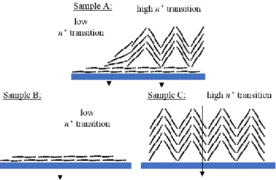
Figure 8. Schematic representation of the molecular orientation for Samples A, B & C.
For Sample C, there is no difference between the edge and the top of the organic mount. 𝜋∗ transition is as high as the top of the not-annealed sample (28 – 31%) with a 𝜋DIP∗ which remains high (12 – 14%). The
mounds are totally crystallized from the first layers deposited. The substrate temperature brings enough energy to start crystallization and overcome molecule-substrate interaction.
Therefore, we obtained with these samples, two opposed molecular orientations: one which present parallel molecules on top of the surface (Sample B) and another in which the organic mounds are directly crystallized as soon as deposited on the substrate (Sample C) (Figure 8). We are thus able to tailor the molecular orientation (thanks to the evaporation conditions). With the perspective of organic electronics, it is important to control the morphology and the molecular orientation to enhance for example the charge mobility through the organic layer.
2.3 Photovoltaic response
We are comparing three OSCs (the process is described in Supporting information Figure S4) with an active layer of P3HT:PCBM, with a “thin” (0.3×10¹⁵
molecule · cm−2), a “thick” (1 × 10¹⁵ molecule · cm−2)
layers of DIPO-Ph4 and a reference based on
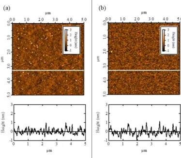
PEDOT:PSS (5 nm), all three as interfacial layers. Prior to characterization of the photovoltaic cells we ensured that the structuration obtained onto ITO (an oxide surface) was comparable to the one obtained onto Si3N4 (see Figure S5). The ITO and Si3N4 have a
native oxide layer and present a similar roughness (< 1 nm), the surface energy is assumed to equivalent following the literature. [29,31] In addition, the
ITO/DIPO-Ph4 interface has already been structurally
and electronically described. [32] As interfacial layer, DIPO-Ph4 layer will act as a hole-transport and an
electron blocking layer. Concerning the solar cell stack, it is worth to note that on top of the DIPO-Ph4 layer a
thin layer (5 nm) of PEDOT:PSS was deposited to prevent the organic solvent of P3HT:PCBM deposition to modify the DIPO-Ph4 morphology.
The photovoltaic cell performances are given in Table 3. The thick DIPO-Ph4 layer reaches 3.1% of as
maximum power conversion efficiency (𝑃𝐶𝐸) using a solar simulator calibrated at 100 mW·cm−2. The open
circuit voltage (𝑉𝑂𝐶) and the fill factor (𝐹𝐹) are 586 mV
and 44%, respectively. The current density (𝐽𝑆𝐶) is 12.1
mA·cm−2 (see Figure 9 and Table 3). These results were
compared to a reference cell using only 5 nm PEDOT:PSS as interfacial layer prepared in the same conditions and which shows a lower 𝐽𝑆𝐶 (11.1
mA·cm−2) and a lower 𝑃𝐶𝐸 at 2.2%. Using DIPO-Ph4
as interfacial layer, we increase the overall yield by 47%. The thicknesses of the DIPO-Ph4 layers have no
effect on the 𝑉𝑂𝐶 . Indeed, this parameter mainly
depends on the LUMO donor/HOMO acceptor difference in the active layer.
In addition to the performance, we extracted the physical constants from the 𝐽 - 𝑉 curve under illumination (see Figure S6). The series resistance decreases to 7 Ω∙cm² when for the reference cell the value was measured at 22 Ω∙cm² and 14 Ω∙cm² for the thinnest IFL based on DIPO-Ph4. On the other side the
shunt resistance ( 𝑅𝑠ℎ ), which reflects the electrical
short-cut and more generally the overall electronical recombination at the interface, remained the same for the three layers, enough high to avoid shortcut losses.
The DIPO-Ph4 layer demonstrates a favorable hole
transport collection at the ITO anode which is consistent with the electronic behavior of DIPO-Ph4.
Figure 9. Photovoltaic characterization with 3 different IFLs
under 100 mW· cm−2; main graphic corresponds to the fourth
quadrant part of the general measurement, in inset (DIPO is for DIPO-Ph4)
Table 3. PV Parameters (100 mW·cm−2) of devices with different
IFLs and P3HT:PCBM as active layer (Units: 𝑃𝐶𝐸 and 𝐹𝐹 (%); 𝑉𝑂𝐶 (mV); 𝐽𝑆𝐶.(mA∙cm-2); 𝑅𝑠ℎ and 𝑅𝑠 (Ω·cm2)). IFLs 𝑷𝑪𝑬 𝑽𝑶𝑪 𝑱𝑺𝑪 𝑭𝑭 𝑹𝒔𝒉 𝑹𝒔 PEDOT: PSS 2.2 583 11.1 34 174 22 DIPO-Ph4 thin 2.3 534 10.5 41 191 14 DIPO-Ph4 thick 3.1 586 12.1 44 191 7
We thus observe a 𝐽𝑆𝐶 increase of 1 mA·cm−2 due to
the lowering of the series resistance and thus an increase of the charge carrier collection. The increase of the fill factor reveals a better electronic process at the interface. Besides, less number of holes are recombined to be collected at the ITO electrode due to the electron blocking effect with the DIPO-Ph4 layer.
[32] As hole transport layer and compared to PEDOT:PSS, our organic layer increases the efficiency of charge collection at the ITO anode. On thick DIPO-Ph4, it is worth to notice that the fill factor increases
significantly despite the surface mounds. Often a highly-structured surface is frequently associated to a rough surface and a bad layer contact which leads to a lower field factor. [33] In the present case, the island structuration leads to a better coverage of the substrate (from 20% for the “thin” layer to 55% for the “thick” layer) and to well-crystallized islands as demonstrated by STXM.
Conclusions
We have shown that STXM is a powerful characterization technique to access the local organization of molecular domains. By decomposing the resulting absorption spectra, in association with the very high lateral resolution we have been able to distinguish different molecular organizations. Thanks to calculations, the electronic transitions observed by X-ray absorption have been attributed to specific 𝜋-𝜋 interactions. These are related to the molecular orientation which in turn is a function of the deposition thickness. The structuration of the thick layer leads to a herringbone 3D structuration. Because of the core crystallinity due to herringbone, an overlapping of the 𝑝𝑧 orbital is induced. Photovoltaic devices with DIPO-Ph4 as interfacial
layer were characterized and compared to a reference cell. Overall performance of the thick DIPO-Ph4 layer
had been the best. The good series resistance demonstrates an improvement of the hole charge transport through this layer. The fill factor proves that the crystalline mounds, despite the 3D surface clusters, is benefit to the performance. Therefore, the short-circuit current increases.
Acknowledgements
QA thanks the LABEX MiChem for funding his PhD grant and the great help during the experiments of HERMES team (SOLEIL).
Electronic Supplementary Material: Supplementary
material (organic material elementary analysis, tilted experiment on sample A, photovoltaic device process, morphology on ITO substrate and equivalent resistant for the organic solar cell) is available in the online version of this article at
http://dx.doi.org/10.1007/s12274-***-****-*
(automatically inserted by the publisher).
References
[1] Li, S.; Ye, L.; Zhao, W.; Zhang, S.; Mukherjee, S.; Ade, H.; Hou, J. Energy-Level Modulation of Small-Molecule Electron Acceptors to Achieve over 12% Efficiency in Polymer Solar Cells. Adv. Mater. 2016, 28 (42), 9423– 9429.
[2] Zhao, J.; Li, Y.; Yang, G.; Jiang, K.; Lin, H.; Ade, H.; Ma, W.; Yan, H. Efficient Organic Solar Cells Processed from Hydrocarbon Solvents. Nat. Energy 2016, 1 (2), 15027. [3] Yan, Y.; Liu, X.; Wang, T. Conjugated-Polymer Blends
for Organic Photovoltaics: Rational Control of Vertical Stratification for High Performance. Adv. Mater. 2017, 29 (20), n/a-n/a.
[4] Lin, Y.; Chen, B.; Zhao, F.; Zheng, X.; Deng, Y.; Shao, Y.; Fang, Y.; Bai, Y.; Wang, C.; Huang, J. Matching Charge Extraction Contact for Wide-Bandgap Perovskite Solar Cells. Adv. Mater. 2017, 1700607.
[5] Yue, S.; Lu, S.; Ren, K.; Liu, K.; Azam, M.; Cao, D.; Wang, Z.; Lei, Y.; Qu, S.; Wang, Z. Insights into the Influence of Work Functions of Cathodes on Efficiencies of Perovskite Solar Cells. Small 2017, 13 (19), n/a-n/a. [6] Atxabal, A.; Braun, S.; Arnold, T.; Sun, X.; Parui, S.; Liu,
X.; Gozalvez, C.; Llopis, R.; Mateo-Alonso, A.; Casanova, F.; et al. Energy Level Alignment at Metal/Solution-Processed Organic Semiconductor Interfaces. Adv. Mater. 2017, 29 (19), n/a-n/a.
[7] Yao, H.; Cui, Y.; Yu, R.; Gao, B.; Zhang, H.; Hou, J. Design, Synthesis, and Photovoltaic Characterization of a Small Molecular Acceptor with an Ultra-Narrow Band Gap. Angew. Chemie - Int. Ed. 2017, 56 (11), 3045–3049. [8] Giebink, N. C.; Wiederrecht, G. P.; Wasielewski, M. R.; Forrest, S. R. Thermodynamic Efficiency Limit of Excitonic Solar Cells. Phys. Rev. B - Condens. Matter Mater. Phys. 2011, 83 (19), 195326.
[9] Yeo, J. S.; Yun, J. M.; Kang, M.; Khim, D.; Lee, S. H.; Kim, S. S.; Na, S. I.; Kim, D. Y. An Approach for an Advanced Anode Interfacial Layer with Electron-Blocking Ability to Achieve High-Efficiency Organic Photovoltaics. ACS Appl. Mater. Interfaces 2014, 6 (22), 19613–19620.
[10] Irwin, M. D.; Buchholz, D. B.; Hains, A. W.; Chang, R. P. H.; Marks, T. J. P-Type Semiconducting Nickel Oxide as an Efficiency-Enhancing Anode Interfacial Layer in Polymer Bulk-Heterojunction Solar Cells. Proc. Natl. Acad. Sci. 2008, 105 (8), 2783–2787.
[11] Zeng, H.; Zhu, X.; Liang, Y.; Guo, X. Interfacial Layer Engineering for Performance Enhancement in Polymer Solar Cells. Polymers (Basel). 2015, 7 (2), 333–372. [12] Berny, S.; Tortech, L.; Véber, M.; Fichou, D.
Dithiapyrannylidenes as Efficient Hole Collection Interfacial Layers in Organic Solar Cells. ACS Appl. Mater. Interfaces 2010, 2 (11), 3059–3068.
[13] Watts, B.; Schuettfort, T.; McNeill, C. R. Mapping of Domain Orientation and Molecular Order in Polycrystalline Semiconducting Polymer Films with Soft X-Ray Microscopy. Adv. Funct. Mater. 2011, 21 (6), 1122–1131.
[14] Bartelt, J. A.; Beiley, Z. M.; Hoke, E. T.; Mateker, W. R.; Douglas, J. D.; Collins, B. A.; Tumbleston, J. R.; Graham, K. R.; Amassian, A.; Ade, H.; et al. The Importance of Fullerene Percolation in the Mixed Regions of Polymer-Fullerene Bulk Heterojunction Solar Cells. Adv. Energy Mater. 2013, 3 (3), 364–374.
[15] Collins, B. A.; Li, Z.; Tumbleston, J. R.; Gann, E.; McNeill, C. R.; Ade, H. Absolute Measurement of
Domain Composition and Nanoscale Size Distribution Explains Performance in PTB7:PC 71 BM Solar Cells.
Adv. Energy Mater. 2013, 3 (1), 65–74.
[16] Stuart, A. C.; Tumbleston, J. R.; Zhou, H.; Li, W.; Liu, S.; Ade, H.; You, W. Fluorine Substituents Reduce Charge Recombination and Drive Structure and Morphology Development in Polymer Solar Cells. J. Am. Chem. Soc.
2013, 135 (5), 1806–1815.
[17] Ye, L.; Zhang, S.; Ma, W.; Fan, B.; Guo, X.; Huang, Y.; Ade, H.; Hou, J. From Binary to Ternary Solvent: Morphology Fine‐tuning of D/A Blends in PDPP3T‐ based Polymer Solar Cells. Adv. Mater. 2012, 24 (47), 6335–6341.
[18] Swaraj, S.; Wang, C.; Yan, H.; Watts, B.; Lüning, J.; McNeill, C. R.; Ade, H. Nanomorphology of Bulk Heterojunction Photovoltaic Thin Films Probed with Resonant Soft X-Ray Scattering. Nano Lett. 2010, 10 (8), 2863–2869.
[19] Collins, B. A.; Cochran, J. E.; Yan, H.; Gann, E.; Hub, C.; Fink, R.; Wang, C.; Schuettfort, T.; McNeill, C. R.; Chabinyc, M. L.; et al. Polarized X-Ray Scattering Reveals Non-Crystalline Orientational Ordering in Organic Films. Nat. Mater. 2012, 11 (6), 536–543. [20] Collins, B. A.; Gann, E.; Guignard, L.; He, X.; McNeill,
C. R.; Ade, H. Molecular Miscibility of Polymer−Fullerene Blends. J. Phys. Chem. Lett. 2010, 1 (21), 3160–3166.
[21] Chasseau, D.; Gaultier, J.; Hauw, C.; Fugnitto, R.; Gianis, V.; Strzelecka, H. Tétraphényldipyranylidène (Dip ϕ 4 ).
Acta Crystallogr. Sect. B Struct. Crystallogr. Cryst. Chem.
1982, 38 (5), 1629–1631.
[22] Fichou, D.; Tortech, L.; Alaaeddine, M. Nouveau Procédé de Fabrication de Dispositifs Électroniques Organiques, 2014.
[23] Alizon, J.; Blanc, J.; Gallice J.; Robert, H.; Fabre, C.; Strzelecka, H.; Rivory, J.; Weyl, C. Organic Conductors and Semiconductors; Pál, L., Grüner, G., Jánossy, A., Sólyom, J., Eds.; Lecture Notes in Physics; Springer Berlin Heidelberg: Berlin, Heidelberg, 1977; Vol. 65. [24] D’Andrade, B. W.; Datta, S.; Forrest, S. R.; Djurovich, P.;
Polikarpov, E.; Thompson, M. E. Relationship between the Ionization and Oxidation Potentials of Molecular Organic Semiconductors. Org. Electron. physics, Mater. Appl. 2005, 6 (1), 11–20.
[25] Barth, V. Dipyrrométhènes Métallés (Co,Ni,Cu) et Dipyrannilidènes : De Nouveaux Matériaux Organiques Pour La Conversion Photovoltaïque de L’énergie Solaire, Paris 6, 2014.
[26] Berny, S.; Tortech, L.; Fichou, D. Derives de Type Dipyrannylidene Comme Couche Interfaciale Anodique Dans Des Dispositifs Electroniques. 2011.
[27] aXis2000 source
http://unicorn.mcmaster.ca/aXis2000.html (accessed May 2, 2017).
Surface Sciences; Springer Berlin Heidelberg: NewYork, Heidelberg, 1992; Vol. 25.
[29] Liu, L.-H.; Michalak, D. J.; Chopra, T. P.; Pujari, S. P.; Cabrera, W.; Dick, D.; Veyan, J.-F.; Hourani, R.; Halls, M. D.; Zuilhof, H.; et al. Surface Etching, Chemical Modification and Characterization of Silicon Nitride and Silicon Oxide—selective Functionalization of Si 3 N 4
and SiO 2. J. Phys. Condens. Matter 2016, 28 (9), 94014.
[30] Venables, J. A.; Spiller, G. D. T.; Hanbucken, M. Nucleation and Growth of Thin Films. Reports Prog. Phys. 1984, 47 (4), 399–459.
[31] Kim, J. S.; Friend, R. H.; Cacialli, F. Surface Energy and Polarity of Treated Indium–tin–oxide Anodes for Polymer Light-Emitting Diodes Studied by
Contact-Angle Measurements. http://oasc12039.247realmedia.com/RealMedia/ads/clic k_lx.ads/www.aip.org/pt/adcenter/pdfcover_test/L- 37/1279441103/x01/AIP-PT/JAP_ArticleDL_060717/jap.jpg/434f71374e315a55 6e61414141774c75?x 1999.
[32] Arnoux, Q.; Boucly, A.; Barth, V.; Benbalagh, R.; Cossaro, A.; Floreano, L.; Silly, M. G.; Sirotti, F.; Derat, E.; Carniato, S.; et al. Energy Level Alignment of a Hole-Transport Organic Layer and ITO: Towards Applications for Organic Electronic Devices. ACS Appl. Mater. Interfaces 2017, acsami.7b06691.
[33] Gupta, D.; Mukhopadhyay, S.; Narayan, K. S. Fill Factor in Organic Solar Cells. Sol. Energy Mater. Sol. Cells 2010, 94 (8), 1309–1313.
Electronic Supplementary Material
X-ray microscopic investigation of Molecular Orientation in a
Hole Carrier Thin Film for Organic Solar cells
Quentin ARNOUX,1,2,3 () Benjamin WATTS,4 Sufal SWARAJ,5 François ROCHET,1,5 Ludovic TORTECH,2,3 ()
1 Sorbonne Universités, UPMC Univ Paris 06, UMR 7614, Laboratoire de Chimie Physique Matière et Rayonnement (LCPMR), F-75005
Paris, France.
2 Sorbonne Universités, UPMC Univ Paris 06, UMR 8232, Institut Parisien de Chimie Moléculaire (IPCM), F-75005, Paris, France. 3 CEA Saclay, IRAMIS, NIMBE (UMR 3685), Laboratoire d'Innovation en Chimie des Surfaces et Nanosciences (LICSEN), F-91191
Gif-sur-Yvette, France.
4 Paul Scherrer Institute, 5232 - Villigen Psi, Switzerland.
5 Synchrotron SOLEIL, L’Orme des Merisiers, Saint-Aubin, BP 48, F-91192 Gif-sur-Yvette, France.
Supporting information to DOI 10.1007/s12274-****-****-* (automatically inserted by the publisher)
Table S1. Elementary analysis of DIPO-Ph4
Atom 1st measurement 2nd measurement Theoretical value
Carbon (%) 86.45 86.17 87.90
Hydrogen (%) 5.12 5.22 5.21
Figure S2. STXM images in thickness at photon energy 285 eV of the not-annealed sample with QB-coverage of 1×10¹⁵ molecule·cm−2
and a tilted incidence angle.
Figure S3. Sample A with a tilted incidence angle: (a) STXM decomposition mapping; (b) Absorption spectra extracted for each region
(the substrate (Sub) spectrum is not represented as there is no absorption from this region); (c) 𝜋∗ area after substraction of the error
function background and the 𝜎∗ area.
Table S2. Experimental 𝜋∗ transitions for the not-annealed sample with a tilted incidence angle, FWHM of the Gaussian contribution
and 𝜋∗/𝜎∗ ratio. Sample/Region 𝝅 ∗/𝝈∗ (%) 𝝅𝐃𝐈𝐏∗ 𝝅𝐏𝐡∗ 𝝅𝐃𝐈𝐏+𝐏𝐡∗ 𝚺 Not-annealed (tilted) Top 12 3 15 30 E2 11 2 16 29 E1 9 3 15 28
Photovoltaic devices:
Figure S4. Schema of the ITO/DIPO-Ph4/PEDOT:PSS/P3HT:PCBM/LiF solar cell.
Commercial ITO substrates (SOLEMS) used have a sheet resistance of 25 Ω·sq-1. As solar cells efficiency relies on
the good quality of the layers and of the interfaces, ITO is firstly cleaned before being exposed to the first organic layer. Wet cleaning was achieved by sequential ultrasonic baths using alkaline detergent solution (5 vol% in deionized water), dichloromethane, ethanol, and isopropanol, each for 10 minutes. The chemically cleaning procedure leaves a weak carbon contamination. The dried surface is then exposed to UV-ozone treatment for 10 minutes. A too long UV ozone cleaning could result in the degradation of the molecular layer deposition due to the formation of active oxygens.
The photovoltaic device structure is ITO/DIPO-Ph4/PEDOT:PSS/P3HT:PCBM/LiF (see Figure S4). The cleaned
ITO substrates are immediately transferred into nitrogen glove box and then used to build the devices.
Figure S5. AFM images: ITO/DIPO-Ph4 samples with QB-coverage of (a) 0.3×10¹⁵ molecule·cm−2; (b) 1×10¹⁵ molecule·cm−2.
DIPO-Ph4 is deposited on ITO under vacuum (see Figure S5) as the same process already described in Sample
preparation part (DIPO-Ph4 on Si3N4). PEDOT:PSS is spin-coated and heated at 140°C for 10 minutes in nitrogen
glove box and a thickness of approximately 5 nm is achieved. The 100 – 150 nm active layer consisting of P3HT:PCBM (15 mg·mL-1 for P3HT, 12 mg·mL-1 for PCBM, blended in ortho-dichlorobenzene) is spin-coated and
subsequently annealed at 80°C for 15 minutes in nitrogen glove box. Then, we transport samples into high vacuum chamber to evaporate LiF (1.0 – 1.5 nm, at rates of 0.01 Å·s−1) and Al (100 – 150 nm, at rates of 0.5 Å·s−1)
and post annealing is performed. The post-annealing consists in firstly heating at 100°C for 10 minutes and then at ~ 150°C for 5 minutes.
The photo-electrical characterization of OPVs is performed using a xenon lamp, with an AMG 1.5 filter. The calibration demonstrates an incident light of 100 mW·cm−2.
The typical 𝐽- 𝑉 curve and the equivalent circuit cell is shown in Figure S6a). In this schema, 𝑅𝑆 is the total
resistance of all the layers. 𝑅𝑆ℎ represents current leakage, such as impurity induced or 𝑝-𝑛 junction leakage.
From a graphical point of view, the value of 𝑅𝑆 can be approximated from the inverse slope of the 𝐽- 𝑉 curve
at forward bias, while 𝑅𝑆ℎ is the inverse slope of the 𝐽- 𝑉 curve at reverse bias.
Figure S6. Representation of (a) a typical 𝐽-𝑉 curve and the equivalent electrical circuit; (b) series and shunt resistance represented as the inverse 𝐽-𝑉 curve.
————————————