HAL Id: cea-01936725
https://hal-cea.archives-ouvertes.fr/cea-01936725
Submitted on 27 Nov 2018
HAL is a multi-disciplinary open access
archive for the deposit and dissemination of
sci-entific research documents, whether they are
pub-lished or not. The documents may come from
teaching and research institutions in France or
abroad, or from public or private research centers.
L’archive ouverte pluridisciplinaire HAL, est
destinée au dépôt et à la diffusion de documents
scientifiques de niveau recherche, publiés ou non,
émanant des établissements d’enseignement et de
recherche français ou étrangers, des laboratoires
publics ou privés.
2D vertical field-effect transistor
Daniela Di Felice, Yannick Dappe
To cite this version:
Daniela Di Felice, Yannick Dappe. 2D vertical field-effect transistor. Nanotechnology, Institute of
Physics, 2018, 29, pp.505708. �10.1088/1361-6528/aae406�. �cea-01936725�
Nanotechnology
PAPER
2D vertical field-effect transistor
To cite this article: D Di Felice and Y J Dappe 2018 Nanotechnology 29 505708
View the article online for updates and enhancements.
2D vertical
field-effect transistor
D Di Felice and Y J Dappe
1Service de Physique de l’Etat Condensé, DSM/IRAMIS/SPEC, CNRS UMR 3680, CEA Saclay, Université Paris-Saclay, F-91191 Gif-Sur-Yvette, France
E-mail:[email protected]
Received 23 July 2018, revised 18 September 2018 Accepted for publication 25 September 2018 Published 17 October 2018
Abstract
Within the framework of 2D materials, we present four theoretical models of a verticalfield-effect transistor(FET) composed of simple alternate graphene and MoS2layers. The electronic transport
properties at a specific graphene/MoS2interface in each configuration are investigated by
focusing in particular on the current as a function of the gate voltage. The gate voltage, simulated with a shift of the bands of a specific layer, allows us to tune the current at the interface and the charge transfer between the planes. This analysis of the charge transfer as a function of the gate voltage reveals a strong connection with the transport characteristics as the slope of the current curve. The analysis of physical phenomena at the graphene/MoS2interface can further improve
the 2D vertical FET performance and contribute to the development of new 2D nanotechnology. Keywords: graphene and 2D materials, density functional theory, electronic transport, transistor (Some figures may appear in colour only in the online journal)
1. Introduction
The field-effect transistor (FET) is an electronic device representing the basic building block of modern technology based on semiconductor electronics. It consists of an elec-tronical device used to amplify or switch the current, com-posed of a semiconductor channel connected with two metallic contacts, where theflowing current can be tuned by applying an electricfield. Generally speaking, the progress of information and communication technology comes from the effort in improving the performances of this electronic component[1]. Traditionally, FETs are based on bulk or 3D
semiconductor channels composed of silicon, and GaAs and GaN semiconductors. Following Moore’s law, which in 1965 predicted that the density of transistors in a chip will double every two years [2–5], the 3D materials have been scaled
down to nanoscale dimension over the pastfive decades. Of course, there is a limit to the size reduction of 3D FETs related to short-channel [6, 7] and surface effects, due to
dangling bonds, which cause the deterioration of transistor performance. After the discovery of graphene [8, 9], many
other graphene-like materials such as germanene, silicene and transition metal dichalcogenides started to be included in electronic devices to overcome some of the previously cited undesired effects.
Many 2D FETs, mostly based on graphene due to its extraordinary properties, have been built or theoretically modeled in recent years. However, graphene does not present any gap, which is strictly necessary in electronics. One way to overcome this problem is to combine graphene with a 2D semiconductor such as MoS2 in a van der Waals (vdW)
heterostructure, a vertical stacking of different 2D materials able to keep the main characteristics of each material[10]. In
an FET architecture, the 2D materials can play the role of an in-plane channel[11,12] or barrier [13–16]. In principle, for a
tunneling transistor such as that proposed by Britnell et al, graphene is used because of the low density of states(DOS), responsible for the greater increase of EF with respect to
conventional 2D gas with parabolic dispersion, as a gate voltage is applied [17–21]. However, the absence of a band
gap in graphene affects the performance of the transistor, due to the low ON/OFF ratio. Recently, an FET fully composed of 2D materials was built with graphene contacts, hBN di-electric and MoS2channel, exhibiting good performance[22].
In this work, we present a very simple model for FET bases on the interface graphene-MoS2monolayer, where the
two monolayers are used as the source-drain electrodes. The MoS2monolayer is included because of its band gap, used to
switch ON/OFF the device. By means of density functional theory (DFT) and non-equilibrium Green’s function formal-ism, we are able to simulate the effect of the gate voltage and calculate the transverse current between the graphene and
Nanotechnology Nanotechnology 29(2018) 505708 (11pp) https://doi.org/10.1088/1361-6528/aae406
1
Author to whom any correspondence should be addressed.
MoS2. Despite the used approximations and its simplicity,
this model is able to reproduce the transistor operations, allowing the complete investigation of the electronic transport at the graphene-MoS2interface. In particular, we focus on the
modification of the transport current, modulated by the gate voltage, between the electrodes when additional alternate layers of graphene and MoS2are stacked on top of them.
Then, a mixed heterostructure (hBN/graphene/MoS2)
and the interface graphene/hBN are also presented to demonstrate the independence of the interfaces and the role of the band edge shape in the transport parameters. We believe that this kind of study is necessary to define the possible role of the vertical vdW heterostructures in the new FET generation.
2. Method of calculation
All the results we present in this work have been obtained within DFT methodology. Both the self-consistency and transport calculations are performed within the Fireball code, a very efficient DFT-localized orbital method [23,24]. This
code uses a self-consistent version of the Harris–Foulkes local density approximation(LDA) functional [25,26] and the
self-consistency is achieved over the occupation numbers. The unit cell optimization and inclusion of the vdW interaction using the LCAO-S2+ vdW approach are presented in detail in appendixA.
Then, using the Hamiltonian calculated within the Fire-ball methodology, the electronic current can be estimated following the non-equilibrium Green’s function technique developed by Keldysh [27]. The complete system can be
virtually separated for the current calculation into two sub-systems(even though the whole system is fully diagonalized in Fireball) given by the different layers and labeled T and S. These two parts are joined in the current equation through a mutual interaction (TTS and TST, which correspond to the
hopping integrals calculated in the Fireball code).
I e h T D T eV D eV d 4 Tr , 1 E E eV TS SS SSr ST TT TTa 2 F F
ò
p r w w r w w w = -´ -+ [ ( ) ( ) ( ) ( )] ( ) where ρTT and ρSS are the density matrices of the twosubsystem, respectively; DTTa ={ ˆI -T gˆST TTˆ ( ) ˆ ˆ ( )}a w T gTS SSa w -1
and DSSr ={ ˆI -T gˆST TTˆ ( ) ˆ ˆ ( )}r w T gTS SSr w -1matrices are related
to the multiple scattering effect produced by potential elec-tronic reflections that could occur when the two subsystems are close to each other. The two terms gˆSS TTr a are the Green’s function for the non-interacting case. The final equation is obtained at 0 K temperature and a bias voltage V. A complete description of the methodology can be found in[28].
To simulate the gate voltage and effect of the band shifting, we used a scissor operator [29, 30] described in
appendixB, able to move each bandεα(k) a valueDa( ).k
In this work, we consider four different stacking con-figurations based on MoS2 and graphene planes. Since
graphene and MoS2 have different lattice parameters, it is
necessary to build a supercell commensurate with both MoS2
and graphene. In particular, our bricks to build the four supercells are composed of four MoS2 and seven graphene
unit cells mutually rotated by 15 degrees. Due to the periodic boundary conditions and the mismatch of the lattice para-meters, a strain on graphene is present, since we keep the MoS2 in its optimized configuration. In fact, the strain on
graphene does not affect the electronic and transport proper-ties, unlike what happens in strained MoS2. As we
demon-strated in a previous work[31], the orientation between the
layers in a heterostructure where the interlayer force is the weak vdW interaction, does not affect the global electronic properties. This suggests that any oriented supercell is equivalent from the global transport point of view. Hence, we will use the smallest possible unit cell in order to reduce the calculation time, since we know that the orientation between the layers does not affect the electronic transport properties of the interface.
3. Results
In this model, the main idea is to combine the gap of MoS2
with the graphene characteristics, using these two 2D crystals as electrodes. The transverse current between graphene and the MoS2 electrodes, ISD, is allowed by the voltage applied
between the two layers, called the source-drain voltage VSD,
and it can be tuned or switched by means of a second voltage VG, able to modify the band alignment between the two
planes. The gate voltage VGis responsible for the shift of the
bands of graphene with respect to the gap of MoS2, simulated
by applying the scissor operator on it, which represents the effective gate potential felt by graphene(normally reduced by ∼100 times with respect to the real applied gate potential when a dielectric of 300 nm of SiO2 is placed between the
gate and the electrode).
The transverse current ISD occurs only if there are
accessible states on both electrodes. In graphene, there are always available electrons(except at the Dirac point) for the current, whereas in MoS2, due to the gap, the current is
possible only if we fall into the conductance band (CB) or valence band(VB). For a specific range of VGcorresponding
to the gap value, the band alignment is such that the Fermi level falls in the gap of MoS2and the current is forbidden; out
of this range, the Fermi level approaches the CB(or VB) and the device switches to the ON state. The Fermi level on the VB and CB leads to a charge transfer(Q) between graphene and MoS2, or in other words to a charge redistribution
between the planes, that is found to be at the basis of the device operation.
In the following, we willfirst analyze the characteristics of the simple graphene/MoS2heterostructure as a transistor
and then we stack additional layers forming further systems as graphene/MoS2/graphene with VG applied on the first
3.1. Band alignment in graphene/MoS2heterostructure
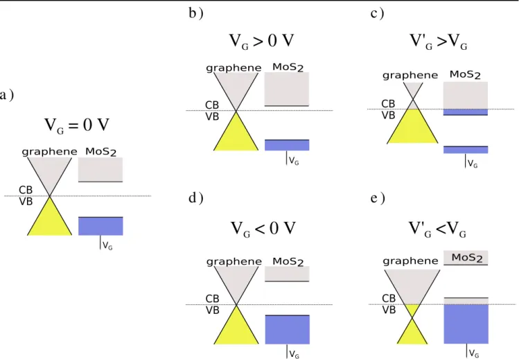
We start by describing the effects of the band alignment in the graphene/MoS2interface shown infigure1. Starting from the
initial position, namely for VG=0 V, the Dirac point falls in
the MoS2gap (at −0.6 V from the CB), and moves towards
the CB as the voltage positively increases, or towards the VB when VGis negative. For positive gate voltages, the graphene
bands shift to higher values; the Fermi level defined by gra-phene moving towards the CB, as can be seen infigure1(b).
For more positive voltages, the Fermi level moves on the CB and a migration of electrons from graphene to MoS2occurs
(see figure 1(c)), providing the accessible states for the
current.
In the case of negative VG, we have an opposite shift and
the migration of electrons from MoS2 to graphene occurs
when the Fermi level falls on the VB (compare figures1(c)
and (e)). In the following sections, we will refer to this migration of electrons from graphene to MoS2as the charge
transfer Q on MoS2and vice versa.
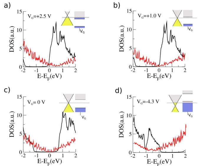
In order to understand the mechanism of our transistor, it is necessary to take a look at the band shift, by means of the DOS alignment for different VG. First of all, we observe that
the shift of the graphene DOS with respect to the MoS2DOS
as a function of VGis not linear, but depends on the position
of the Fermi level(falling almost in correspondence with the
Dirac point), with respect to the MoS2gap, to the CB and VB.
Hence, when the Fermi level falls in the MoS2 gap, an
increase of the gate voltage of 1 V (from 0 to +1.0 V in figures 2(b) and (c)) yields a shift of the band structure of
almost 0.7 eV. On the other hand, when the Fermi level approaches the CB (or VB), the same VGincreased by 1 V,
which causes a reduced shift of the DOS, since a charge transfer from graphene to MoS2(or from MoS2to graphene)
occurs, oppositely to the applied gate. This reaction of the system to the applied band shift on graphene is discussed in appendix B.
This means that, in order to reach thefirst electronic states in CB(VB) of MoS2, and consequently the current saturation,
we need an effective VG, which is larger than the value of the
gap. This is the reason we need to calculate the electric current for a range of VG from −5 to +5 V (larger that the gap of
MoS2). Note that when the Dirac point is in the gap, it defines
the Fermi level, whereas when it is close to CB (VB), the charge transfer from graphene to MoS2 (from MoS2 to
gra-phene) results in an electronic doping of graphene causing a displacement of the Fermi level from the Dirac point.
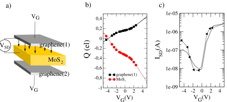
3.2. Graphene/MoS2electronic transport properties
We now move to the quantitative evaluation of the charge transfer for graphene/MoS2 by plotting the Q(VG) curve
Figure 1.Band diagrams: alignment of graphene and MoS2Fermi electronic levels for positive and negative VG, where the Dirac cone falls in the MoS2gap(panel b and c) and for larger absolute values where the the Dirac cone falls in the CB and VB, in panel d) and e), respectively.
3
(see figure3(a) for the structure). As previously mentioned,
the approach of the Fermi level to CB or VB leads to a charge transfer Q between the layers. Infigure3(c), we plot Q at the
interface as a function of VG. This curve shows three regions
characterized by linear behavior with two different slopes. The plateau-like part(with smaller slope) coincides with the Fermi level moving in the MoS2gap, namely for a range of
VGof∼2V, corresponding to the OFF state of the transistor
(here we can still find finite Q=0.18 el/unit cell, even for VG=0 V, coming from the interaction between the layers).
Then, right out of the OFF range of VG, we found the very
important part, we call the switch region, defined as the range of VGwhere the Q curve changes its slope from the OFF to
the ON linear parts, occupying around 1 V in this case; the change of slope does not suddenly occur. For larger VG, we
recover the two second linear regions, for positive and negative voltages. We note that even in the OFF region, we have a charge transfer Q that leads to a non-zero electronic density in the gap of MoS2.
Infigure3(b), we show the behavior of ISD(VSD)
calcu-lated for a range of VSDbetween −0.5 and +0.5 V and for
different VG. For gate voltage VG=−1.0 V, corresponding to
the OFF state of the transistor, the current is very low.
However, when the Dirac cone approaches the VB(CB), for VG<−1.7 V (VG>+0.3 V), we observe an increase of the
positive (negative) branch of the current curve for positive (negative) VSD; this corresponds to the ON state.
In figure3(d), the current ISD(VG) for VSD=−0.1 V is
shown for a VGrange between−5 and +6 V, corresponding
to the range where the ON/OFF switch occurs. Again, in the OFF region around −1.5 and +0.5 V, we found very low current corresponding to the plateau in Q(VG), whereas in
the ON region we can find two important parts: one is the increase of ISD(VG), related to the change of Q slope, and the
other one is the saturation of the current, for VG> 2.0 V and
VG< −3.0 V, corresponding to the second linear region of Q.
The main parameters we want to modify by stacking an additional layer is the slope of ISD(VG) and the ratio between
the higher and lower current, called the ON/OFF ratio, which defines how good the performance of the transistor is.
In this work, the slope of ISD(VG) is defined as the
increase of the current curve in the VGrange from 0 to+2 V,
whereas the ON/OFF ratio is the ratio between the current at VG=5 V and the current at VG=0 V. In this first
config-uration, we found a slope of∼2×10²and an ON/OFF ratio of ∼2.4×10².
Figure 2.DOS and the relative band alignment for different values of VG. Red(black) line corresponds to graphene (MoS2) DOS. Graphene DOS has been multiplied byfive, in order to directly compare the two DOS.
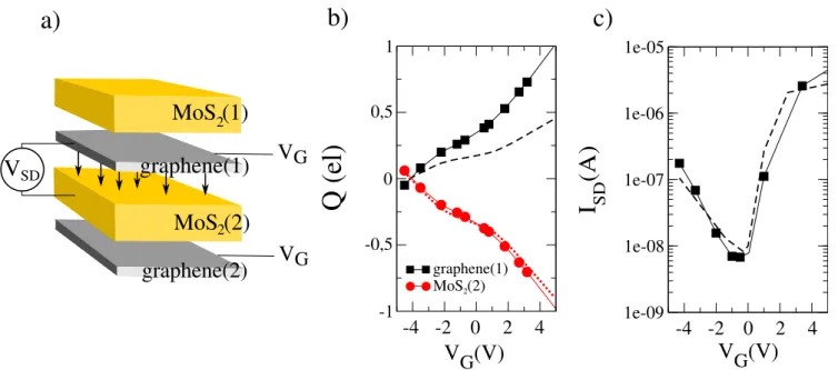
3.3. Graphene/MoS2/graphene heterostructure
Starting from graphene/MoS2heterostructure, we now stack an
additional graphene, obtaining graphene(1)/MoS2/graphene(2)
where, as previously, graphene(1) and MoS2are the source and
drain electrodes(see figure4(a)).
As is known from the previous work[31], the presence of
the second graphene does not affect the electronic properties of the component layers. However, its presence modifies the band alignment, strictly connected to the charge transfer Q, and then to the current. In figure 4(b), we plot Q for each
Figure 3.Graphic representation of the transistor model composed of graphene/MoS2heterostructure is illustrated in(a), the current ISD(VSD) for different VGin(b). Charge transfer with a zoom on the switch region and the current as a function of the gate voltage ISD(VG) for VSD=−0.1 V are shown in (c) and (d), respectively.
Figure 4.Graphic representation of the transistor model composed of graphene(1)/MoS2/graphene(2) heterostructure in (a), charge transfer Q on graphene(1), graphene(2) and MoS2in black, red and green, respectively, are plotted in(b). In (c), ISD(VG) for VSD=−0.1 V is shown together with the current obtained in thefirst case, in a solid and dashed line, respectively.
5
layer, in black, red and green lines for graphene(1), MoS2and
graphene(2), respectively. The dashed lines correspond to the charge transfer on graphene in the original graphene/MoS2
heterostructure. We found that the charge transfer for all three layers is very different from what we had before. The first difference is that Q varies less with respect to VGthan in the
previous graphene/MoS2device, due to the presence of the
second graphene layer. Furthermore, here, we do not have the three linear regions as before and Q on graphene(1) has almost the same slope for the whole VGrange. Looking at Q
on MoS2, however, we can recognize two regions from−5 to
+0.5 V and from +0.5 to +5.0 V, characterized by small and very smooth change of slope.
The transverse current calculated at the graphene(1)-MoS2
interface, ISD(VG), is represented in figure4(c). The change of
Q is reflected in the current behavior: the OFF region seems to be larger, according to the absence of the third linear region in Q for negative VG, and also for positive values, the increase of
ISD is slower than in the previous transistor, as Q increases
slowly. The absence of the change of the switch region for negative VGis reflected in the low current.
In this configuration, the presence of the second graphene layer reduces the effect of VGin the switching of the charge
transfer curve from the OFF to the ON region. In fact, the switch region increases and, consequently, the current shows a smoother increase with respect to graphene/MoS2, clearly
visible since here it is necessary to apply a larger value of VG
of 1 V to recover the same current as in the previous graphene/MoS2 system. This results in a worsening of the
transistor parameter given by the slope of ISD(∼1.4×10²).
However, the ratio between the larger and the lower current appears to be larger than in the previous case, being almost 103. The idea is to try to increase the velocity of the band
shift, which can be analyzed by looking at the Q shape, in particular at the switch between the linear regions, which should be as small as possible to lead to a faster increase of ISD. In other words, we want the Fermi level to move as fast
as possible towards the CB or VB edges of MoS2. We will try
to achieve this by using the heterostructure and by applying the gate voltage on the two graphene layers.
3.4. Double gate on the two graphene layers
By considering the same heterostructure graphene(1)/MoS2/
graphene(2) (figure5), it is possible to make something different;
we apply the same gate voltage in both graphene layers in order to also use the second graphene as an active component, by also shifting its band. This is a symmetric system from the point of view of the band shift, composed by two distinct and equivalent interfaces: graphene(1)-MoS2 and MoS2-graphene(2), being
the first interface where the VSD is applied and the current
calculated.
The symmetric configuration ensures that both graphene layers present the same alignment. The analysis of the charge transfer and the transport characteristics have been repeated in this new configuration and the results are presented in figure5.
First of all, we take a look at the charge transfer. Obviously, wefind the same Q curve on both graphene lay-ers, as we expected from the symmetry of the system. Then, we note that the Q curve corresponds to the one found on graphene in the first configuration (compare the black con-tinuous and dashed lines in figure5(b)), revealing a kind of
independence between the two graphene(1)/MoS2 and
MoS2/graphene(2) interfaces.
Here, the same VGbrings about doubled charge transfer
on the MoS2 electrode with respect to the original
Figure 5.Graphic representation of the transistor model composed of graphene(1)/MoS2/graphene(2) with VGapplied on both graphenes in (a) and charge transfer Q on graphene and MoS2(black and red line, respectively) is shown in (b). In (c), ISD(VG) for VSD=−0.1 V is shown together with the current obtained in thefirst case, in a solid and dashed line, respectively.
graphene/MoS2 interface, in both ON and OFF zones.
However, the switch region is not thinner than in the previous case, which means that the same range of VG as in
MoS2/graphene is necessary to move from the OFF to the
ON part. The consequence is that the increase of the current does not occur faster than before. Consequently, we do not expect a significant improvement of ISD with respect to the
graphene/MoS2 interface, as can be observed when
com-paring the continuous and dashed lines infigure5(c). We also
note that, as a consequence of the Q doubling on the OFF and ON region, the ratio between the two slopes of the Q curve calculated on MoS2characterizing the ON and OFF regions
does not change.
3.5. MoS2/graphene/MoS2/graphene heterostructure
Considering the results of the previous cases, we now move to the last configuration: MoS2(1)/graphene(1)/MoS2(2)/
graphene(2) heterostructure with gate voltage applied on two graphene planes(figure6(a)). The electrodes are graphene(1)
and MoS2(2).
Following our idea, we expect tofind twice the amount of charge transfer Q on both electrodes, as can be seen in figure6(b), where Q on graphene (black line) and Q on the
MoS2 electrodes are shown and compared to the charge
transfer in the simple graphene/MoS2configuration (dashed
line). We confirm that the charge transfer between the layers can be evaluated by considering each interface independently from the others.
Also, in this latter case, we can relate the charge transfer (figure6(b)) and ISD(figure6(c)). We found that the slope of
the current is not improved with the additional MoS2 and
graphene layers, whereas we canfind a larger ON/OFF ratio.
3.6. hBN/graphene, the charge transfer depends on the DOS
At this point, after a complete description of the role of the additional layers in the electronic transport characteristics, we want to focus on the intrinsic parameters affecting the slope of ISD(VG). We show here that the fundamental role is played by
the shape of the DOS in the CB and VB edges. The way the DOS increases, since we do not have a perfect sharp band edge, is reflected on the charge transfer curve, in the switch region and then in the current slope. In the end, the slope ratio between the OFF and ON Q region is a consequence of the DOS shape at the gap edges.
A simple test is performed on the hBN/graphene het-erostructure shown infigure7(a). The hBN is not suitable as
an electrode because of its very large band gap. However, it provides a very clear example to demonstrate how the shape of the CB and VB edges affects the increase of the current.
The switch of the charge transfer from the OFF to the ON linear region of hBN/graphene and graphene/MoS2 (blue
and red lines in figure7(b), respectively) is stressed by the
arrows in the zoom on the right. In hBN/graphene the change of slope from the OFF to the ON region occurs at ∼5 V, whereas for MoS2/graphene it occurs at less than 2 V; this
provides a larger switch region for hBN/graphene. Thus, we expect a smoother increase of the ISDcurve compared to the
current in graphene/MoS2, as shown by the blue and the red
lines, respectively, infigure7(c).
The very slow increase of the charge and, consequently, of the current with respect to the graphene/MoS2 case, is
Figure 6.Graphic representation of the transistor model composed of MoS2(1)/graphene(1)/MoS2(2)/graphene(2) is shown in (a); the charge transfer Q on graphene(1) and MoS2(2) (black and red line, respectively) is compared with the charge transfer obtained in the graphene/MoS2case(dashed lines) with the scissor on graphene in (b). In (c), ISD(VG) for VSD=−0.1 V is shown together with the current obtained in thefirst case, in the solid and dashed line, respectively.
7
related to smoother CB edges of hBN(blue line in figure7(d)
around 1 and 2 eV) with respect to the one of MoS2.
4. Independence of the interfaces in vdW heterostructures
In this brief section, we would like to show the possibility to predict the shape of the charge transfer Q on the intermediate layer in a mixed heterostructure, by considering separately the single interfaces and the charge transfer Q between them. Here, we consider the MoS2/hBN/graphene heterostructure,
which can be decomposed in two different interfaces, MoS2/hBN and hBN/graphene, represented in figure 8(a).
Here, we just compare the sum of the charge transfer Q on graphene calculated in the separate interfaces, 2) + 3), 2) and 3) in figure8(b) (the light and dark green for hBN-graphene
and graphene-MoS2, respectively), with Q on graphene
cal-culated directly in the hBN/graphene/MoS2 heterostructure
(labeled 1) in figure8(b).
Comparing the sum of Q from the separate interfaces and that calculated in the hBN/graphene/MoS2 heterostructure,
2) + 3) and 1) in figure8(b), we find a good agreement in the
shape of the curve, whereas we have a vertical shift of approximately 0.1 electrons. However, as we illustrated in the main text, the shape of Q, in particular, the switch region and the ratio between the slopes in the ON and OFF linear region, are the most important parameters to characterize the current
Figure 7.Graphic representation of the graphene/hBN interface is shown in (a). In (b) the charge transfer Q calculated on the graphene layer
for hBN/graphene (blue line) is compared to the one calculated on graphene in graphene/MoS2(red line); the arrows in the zoom on the right indicate the size of the switch region. In(c) the current calculated at the graphene/hBN interface as a function of VGis indicated by the blue line, whereas the red line is the current corresponding to graphene/MoS2, already shown in previous sections. In(d) the comparison is shown between the partial DOS of MoS2(red solid and dashed lines) and that of hBN (blue line). CB edges have a different shape, smoother in hBN than in MoS2, as shown in the inset.
at the interface. From a computational point of view, the possibility to succeed in this kind of prevision separating the single interfaces, is important because it avoids the problem related to the building of the supercell considering the mis-match between three or more different 2D crystals.
Furthermore, another interesting application of the inde-pendence of the interfaces is illustrated in this last part. Here, we report a simple scheme of a heterostructure composed of alternate graphene and MoS2 planes beyond graphene/
MoS2/graphene/MoS2. We found that the presence of the
further planes does not change the charge transfer on the graphene-MoS2interface in the middle(see figure9(a)).
This kind of independence found in the vdW heterostructure interfaces when the alternate graphene layers are connected to the gate, can be useful if one wants to avoid the charge disper-sion on the electrodes. One possible structure is represented infigure9(b): if we add extra vdW layers on the top and bottom
of MoS2/graphene/MoS2/graphene, as the capper in the
tran-sistor, for instance, the charge transfer necessarily present at the external interfaces does not affect the charge transfer and con-sequently the electronic transport between the electrodes.
5. Conclusions
In conclusion, in this work we have studied the mechanism at the basis of the graphene/MoS2 transistor performance by
observing and comparing the results coming from three het-erostructures of alternate graphene and MoS2 layers. In all
these systems, we have chosen the graphene and MoS2
electrodes where the electronic transport calculations were performed, and we have studied the influence of the addi-tional layers on the performance of the transistors. We have focused our attention on the current modulation as a function
Figure 8.In(a) the hBN/graphene/MoS2heterostructure labeled 1). 2) and 3) are the graphic representations of the single interfaces of hBN/ graphene and graphene/MoS2. In(b) we plot the charge transfer Q on graphene, calculated directly in 1) (red line) and as a sum of the Q calculated on graphene in the 2) and 3) interfaces (light and dark line, respectively). Dashed red line is Q calculated as a sum of the charge transfer in the single interfaces 2) and 3).
Figure 9.In(a) a sequence of alternate graphene-MoS2interfaces is represented, with graphene layers connected to a gate voltage; the charge transfer between the layers is given by a succession of+2Q and −2Q. This demonstrates that the charge transfer on the layers in the middle is affected just by the closer plane and the presence of the farther layers is negligible. In(b) a scheme of the smallest heterostructure (MoS2/graphene/MoS2/graphene) that can be used to avoid the effect of the undesired charge transfer given by external layers (the red objects) on the electrodes is given, in this representation, by the graphene and MoS2in the middle.
9
of the gate voltage, namely ISD(VG), relating its behavior to
the charge transfer Q (and, consequently, to the band shift). We found that the width of the switch region is strictly related to the slope of ISD(VG). The faster the change of slope of the
charge transfer from the OFF to ON region occurs, namely for small VGrange, the more ISD(VG) will rapidly increase.
By stacking additional layers, it is possible to tune the effect of the gate voltage on the band shift and, consequently, on the charge transfer. We have seen that one is able to reduce the effect of VGon the charge transfer and on the current just
by adding an extra graphene layer non-connected to the gate as in the first graphene/MoS2/graphene, worsening the
perfor-mance of the transistor. On the other hand, we can improve the VGeffect on the charge transfer on the electrodes, connecting
also the second graphene to the gate potential. However, even if Q is doubled on the electrodes, the current does not switch faster, since neither the velocity of the Q curve moving from the OFF to the ON region, nor the increased ratio of Q, namely the ratio between the ON and OFF region slope, change. By stacking additional layers, the current can at least show an increase in the ON/OFF ratio, probably due to more charges at the Fermi level, determining the current.
We found that the heterostructures composed of alternate layers beyond the electrodes do not represent the way to really improve the transistor performance. Moreover, further addi-tional planes beyond MoS2/graphene/MoS2/graphene do not
affect even the charge transfer on the electrodes, as a con-sequence of the interface independence. However, this kind of independence found in the vdW heterostructure interfaces when the alternate graphene layers are connected to the gate, can be useful if we want to avoid the charge dispersion on the electrodes. If an extra vdW layers is on the top and bottom of the MoS2/graphene/MoS2/graphene, as the capper in the
transistor, for instance, the necessary charge transfer present at the external interfaces does not affect the charge transfer and consequently the electronic transport between the electrodes.
Moreover, the independence of the interfaces can also be used to study the heterostructures composed of more than two different crystals such as, for example, hBN/graphene/MoS2.
The possibility to separate the two interfaces allows us to avoid the computational problem of the lattice mismatch between three crystals and to build and analyze even different super-cells with a different size for each interface. For example, it is possible to study, within the framework of DFT, transistors with a more complex structure, made by vertical stacking of 2D crystals, just by considering separately each interface.
We can conclude by saying that the mixed vertical het-erostructures composed of more than two different crystals are not useful to improve the performance of the transistor, whereas the choice of the semiconductor with a sharp band edge is more important to increase the current slope for a fast switching device.
Acknowledgments
D Di Felice thanks the CEA Phare Program for funding her research.
Appendix A. Unit cell optimization
The unit cell we used to build the four configurations is composed of graphene/MoS2 mutually rotated 15 degrees,
see figure A1. All the other configurations are built by adding one graphene layer, one MoS2or both in a vertical
stacking.
Following the Fireball formalism based on the self-con-sistent Harris–Foulkes LDA functional, the structural optim-ization is performed until the forces were below 0.1 eV/Å. Optimized numerical basis sets have been used for molyb-denum(Mo), sulfur (S) and carbon (C) with respective cutoff radii in atomic units of s=3.9, p=4.5, d=5.0 for S, s=5.0, p=4.5, d=4.8 for Mo and s=4.5, p=4.5 for C. The choice of the supercells is a well-known problem in DFT codes as already dealt with in our previous article [31] with
respect to the effect of the rotation angle on the electronic properties of graphene/MoS2 heterostructure. Hence, due to
the lattice vector mismatch and rotation angle, a perfect match is very difficult to obtain. Consequently, it is necessary to adapt the lattice vector parameter of graphene and MoS2by
applying an artificial strain on the two layers that can affect the electronic properties. In our previous article, we found a way to treat this problem by studying the effect of the strain on the electronic properties of graphene and MoS2. We found
that the MoS2 electronic gap is very sensitive to the strain,
whereas on graphene electronic structure the effect of the strain is negligible. Consequently, we chose to keep the MoS2
layer in the optimized structure, while graphene presents a small strain. Furthermore, while LDA functional is a good approximation for covalent bonds characterizing the in-plane interactions, the out-of-plane vdW interactions are not well dealt with in DFT. This well-known limit of DFT in dealing with the vdW interaction, is overcome by using the LCAO-S2 + vdW approach [32], based on the dipolar approximation for
vdW interaction. This approach has proved to give good results in agreement with experiments[33–35]. The structural
optimization is thus performed in two steps: a preliminary equilibrium configuration is obtained by using LDA func-tional, and then the LCAO-S2 + vdW approach is used to calculate the equilibrium interlayer distance, found to be ∼3.1 Å,as reported in [31].
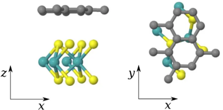
Figure A1.Representation of the basic graphene/MoS2cell used in our calculations.
Appendix B. The scissor operator
The scissor operator consists of an extra potential added to the sub-Hamiltonian written in the localized orbital basis set of a system, in order to shift the electronic levels of the corresp-onding subsystem with respect to the rest of the system. It can be seen as an extra electricfield applied to one subsystem. In the present case, we shift the electronic levels of the graphene monolayer with respect to the levels of MoS2, in order to
reproduce the effect of an electrostatic gate applied to the system. Since this operator is part of the Hamiltonian, the electronic density is correctly recalculated through the usual self-consistent process, and the charge transfer is correctly taken into account. This approximation works very well here due to the weak coupling between the 2D materials through vdW interaction. This method has been developed first for metal/organic interfaces to correct the electronic level mis-alignment [36]. It has then been generalized to extended
interfaces in our previous work[31].
The scissor operator, in the most general case, is able to move each bandεα(k) a value Δα(k). Taking advantage of the properties of projectors, it can be written as:
OS k k k , 2 k ,
å
a a = D ñá a a( )∣ ( ) ( )∣ ( )where∣ ( ) is the eigenorbital with energya kñ εα(k). We will
calculate the matrix elements of the scissor operator in the Fireball basis set for periodic systems:
B N e k 1 , 3 i i r i R k R , ñ =
å
i f,ñ m + m ∣ ( ) ( )∣ ( )where∣f ñm,i is the numeric atomic orbital of the orbitalμ of atom i(at ri). If we expand∣ ( ) in this basis set:a kñ
b B k R k , 4 l l l , , ,
å
a ñ = ñ l l a l ∣ ( ) ( )∣ ( ) ( )the scissor operator matrix element Bá m,i( )∣k O BS∣ n,j( ) takeskñ
the form: B O B B b B k k k k R k , 5 i S j i l l l , , , , , ,
å
å
á ñ = D á ´ ñ ´ m n a a m l l a l ⎛ ⎝ ⎜⎜ ⎞⎠⎟⎟ ( )∣ ∣ ( ) ( ) ( )∣ ( )∣ ( ) ( ) b R B k B k , 6 m m m j , ,,* , ,å
´ á ñ = s s a s n ⎛ ⎝ ⎜⎜ ( ) ( )∣ ∣⎞⎠⎟⎟ ( ) ( ) b b B B B B k R R k k k k , 7 l m l m i l S m j S k k , , , , , , , , , , , i l m j , ; , , ; , *å
D á ñ ´ á ñ a l s a la sa m l s n m l s n ( ) ( ) ( ) ( )∣ ( ) ( )∣ ( ) ( ) ( ) ( )where Sm l, ; ,i l( ) is the overlap matrix element between thek
orbitalμ of atom i and the orbital λ of atom l.
In our calculations, the scissor operator has been applied only on graphene, by selecting the eigenorbitals ∣ ( )a kñ
corresponding to carbon atoms. The initial shift given by Δα(k) is applied on the selected eigenorbitals (all the carbon
orbitals), which build the graphene sub-Hamiltonian. This sub-Hamiltonian is part of the whole Hamiltonian over which the self-consistency is performed. Thus, the whole system reacts to the scissor and the whole electronic density is recalculated. In our specific case, when the self-consistency is reached, the energy shift of the graphene eigenvalues with respect to MoS2is always lower than the appliedΔα(k), as a
consequence of the response of the system. In this work, we refer to the gate voltage as the value ofΔα(k) applied on the graphene eigenorbitals. Thus, VG and Δα(k) have the same
value. Moreover, the value of Δα(k) is the same for all the eigenorbitals where it is applied.
ORCID iDs
Y J Dappe https://orcid.org/0000-0002-1358-3474
References
[1] Schwierz F et al 2015 Nanoscale7 8261
[2] Moore G E 1965 Electronics38 114–77
[3] Dennard R H et al 1974 IEEE J. Solid-State Circuits9 256–68
[4] Mistry K et al 2007 IEEE International Electron Devices Meeting(Washington, DC, 10-12 December 2007)247–50
[5] Cartwright J 2011 Nature38 114–77
[6] Ferrain I et al 2011 Nature479 310–6
[7] Colinge J P 2004 Solid State Electron48 897–905
[8] Novoselov K S et al 2004 Science306 666
[9] Novoselov K S et al 2012 Nature490 192
[10] Geim A K and Grigorieva I V 2013 Nature499 419
[11] Radisavljevic B et al 2011 Nature6 147
[12] Yoon Y et al 2011 Nano Lett.11 3768–73
[13] Myoung N et al 2013 ACS Nano7 7021–7
[14] Britnell L et al 2012 Science335 947
[15] Yu W J et al 2013 Nat. Mater.12 246
[16] Singh A K et al 2016 ACS Appl. Mater. Interfaces8 34699–705
[17] Luryi S 1988 Appl. Phys. Lett.52 201
[18] Heiblum M et al 1990 IBM J. Res. Develop.34 530
[19] Simmons J A et al 1998 J. Appl. Phys.84 5626
[20] Zaslavsky A et al 2003 Appl. Phys. Lett.83 1653
[21] Sciambi A et al 2011 Phys. Rev. B84 085301
[22] Roy T et al 2014 ACS Nano8 6259–64
[23] Lewis J P et al 2011 Phys. Status Solidi B248 1989
[24] Jelínek P et al 2005 Phys. Rev. B71 235101
[25] Harris J 1985 Phys. Rev. B31 1770–9
[26] Foulkes W M C and Haydock R 1989 Phys. Rev. B39 12520–36
[27] Keldysh L V 1964 Zh. Eskp. Teor. Fiz 47 1515 Keldysh L V 1965 Sov. Phys. JEPT20 1018 Mingo N et al 1996 Phys. Rev. B54 2225 [28] Gonzalez C et al 2016 Nanotechnology27 105702
[29] Abad E et al 2010 J. Phys.: Condens. Matter304007
[30] Abad E 2013 Energy Level Alignment and Electron Transport Through Metal/Organic Contacts (Heidelberg: Springer) [31] Di Felice D et al 2017 J. Phys. D: Appl. Phys.50 17LT02
[32] Dappe Y J et al 2006 Phys. Rev. B74 205434
[33] Dau M T et al 2018 ACS Nano12 2319
[34] Pierucci D et al 2016 Sci. Rep.6 26656
[35] Savini G et al 2011 Carbon49 62
[36] Abad E et al 2011 J. Chem. Phys.134 044701
11