HAL Id: hal-00906019
https://hal.archives-ouvertes.fr/hal-00906019
Submitted on 16 Jan 2014HAL is a multi-disciplinary open access archive for the deposit and dissemination of sci-entific research documents, whether they are pub-lished or not. The documents may come from teaching and research institutions in France or abroad, or from public or private research centers.
L’archive ouverte pluridisciplinaire HAL, est destinée au dépôt et à la diffusion de documents scientifiques de niveau recherche, publiés ou non, émanant des établissements d’enseignement et de recherche français ou étrangers, des laboratoires publics ou privés.
P-type and N-type multi-gate polycrystalline silicon
vertical thin film transistors based on low-temperature
technology
Peng Zhang, Emmanuel Jacques, Regis Rogel, Olivier Bonnaud
To cite this version:
Peng Zhang, Emmanuel Jacques, Regis Rogel, Olivier Bonnaud. P-type and N-type multi-gate poly-crystalline silicon vertical thin film transistors based on low-temperature technology. Solid-State Electronics, Elsevier, 2013, 86, pp.1-5. �10.1016/j.sse.2013.04.021�. �hal-00906019�
P-type and N-type multi-gate polycrystalline silicon vertical thin film
transistors based on low-temperature technology
P. Zhang, E. Jacques, R. Rogel*, O. Bonnaud
Département Microélectronique et Microcapteurs, IETR, UMR CNRS 6164, Université de Rennes 1, Campus Beaulieu,
35042 Rennes Cedex, France
* Corresponding author, Tel.: +33 22 3235776; fax: +33 22 3235657
E-mail address: [email protected] (R. Rogel)
ABSTRACT
P-type and N-type multi-gate vertical thin film transistors (vertical TFTs) have been
fabricated, adopting the low-temperature (T ≤ 600°C) polycrystalline silicon (polysilicon)
technology. Stacked heavily-doped polysilicon source and drain are electrically isolated by an
insulating barrier. Multi-teeth configuration is defined by reactive ion etching leading to
sidewalls formation on which undoped polysilicon active layer is deposited. All the
polysilicon layers are deposited from low pressure chemical vapor deposition (LPCVD)
technique. Vertical TFTs are designed with multi gates, in order to have a higher equivalent
channel width. Different active layer thicknesses have been attempted, and an ION/IOFF ratio
slightly higher than 105 is obtained. P-type and N-type vertical TFTs have shown symmetric
electrical characteristics. Different geometrical parameters have been chosen. IOFF is
proportional to the single channel width, and to the tooth number. ION is only proportional to
the tooth number. These devices open the way of a CMOS-like technology.
1. INTRODUCTION
Polycrystalline silicon thin film transistor (polysilicon TFT) has shown its interest in
various applications, such as the solar cells [1], random access memories (RAMs) [2], flat
panels for imaging [3], and especially in the display domains as AMLCD [4] or AMOLED [5].
For these applications, a higher integration density and thus a higher current density are
looked for. Thus, the primary motivation of this work is this target that could be obtained by
adopting a short channel length for the transistors. The vertical thin film transistor (vertical
TFT) enables fabricating transistors with ultra-short channel length that is determined by the
deposited film thickness instead of the lithographic limitation as in its planar counterpart.
Indeed, this limitation is rather high due to large area process and, a better control of the
channel length seems a very exciting issue. Much research has been carried out on polysilicon
VTFTs.
The James D. Flammer's group has fabricated polysilicon VTFTs adopting Arsenic
implanted source and drain, which degrades after annealing [6]. The Tan Fulei's group has
used a bottom gate vertical TFT structure with a self-aligned offset [7], and excimer laser
annealing methods [8] to crystallize the active layer. However, this self-aligned offset
structure requires high temperature, and the high cost and homogeneity are the technological
drawbacks of the laser crystallization. In our work, the VTFTs are fabricated with
low-temperature polysilicon technology, which is compatible with glass substrates, while a
[9], polysilicon VTFTs were fabricated with an undoped polysilicon active layer between two
heavily-doped polysilicon layers (source and drain). However, the large overlapping area
between source and drain has led to a strong off-current, IOFF [9]. In this paper, a novel
polysilicon VTFT structure has been proposed, which eliminates the large overlapping area by
the introduction of an insulating barrier between source and drain. In addition, different
geometrical parameters have been chosen, i.e., different tooth widths, Wt (10 µm and 20 µm),
different numbers of teeth, Nt (1, 2 and 4), and different single channel widths, Wc (10 µm,
20 µm and 30 µm). The key point of the fabrication process lies in the formation of the
continuous sidewalls due to the difference of the etching selectivity between the polysilicon
and the insulating barrier. In this paper, the detailed fabrication process is introduced and
electrical characterizations of the devices are presented, analyzed and discussed, more
especially, the comparison between electrical behaviors of the P-type and N-type VTFTs.
2. DEVICE STRUCTURE AND DESIGN
For the polysilicon VTFTs, the schematic three-dimensional (3D) view is shown in figure
1 (a). The 3D structure enables several gates positioned in parallel, with the gate electrode
passing over all the teeth. Source and drain are discriminated by a partial etching until
reaching the bottom heavily-doped polysilicon layer. The RIE endpoint control is obtained
from a laser interferometer measurement. Fig. 1 (b) shows clearly the cross-sectional view of
a basic tooth structure including two channels. Source and drain contacts are located in front
and behind the cross-sectional plan, and they are electrically isolated by an insulator barrier.
Active layer is deposited after the formation of the tooth sidewalls, the distance between the
length, L, is defined by the barrier thickness located in-between the both heavily doped
polysilicon layers.
3. FABRICATION PROCESS
Thin film technology is adopted to fabricate the devices, and the polysilicon thin films are
the determinant factor for the fabrication of the vertical TFTs. The polysilicon layers are
deposited from LPCVD technique at 550°C and 90 Pa using silane (SiH4) as precursor gas. At
these conditions, the films are still in amorphous state [10]; therefore a solid phase
crystallization step (SPC) is carried out at 600°C for 12 hours to crystallize the amorphous
silicon into polysilicon. The combined techniques of LPCVD and SPC have been adopted in
the lateral TFTs fabrication, combination that was proved to be a way to obtain a high field
effect mobility of carriers higher than 100 cm2/V·s with an ION/IOFF of more than 106 [11].
Therefore, this technology will also be used in our vertical TFTs fabrication. In addition,
in-situ doping can be obtained by adding dopant gases to the precursor gas, SiH4: Phosphine,
PH3, for N-type doping or diborane B2H6 for the P-type. Therefore, P-type and N-type VTFTs
could be easily fabricated in the same run, just by adopting different doping gases for source
and drain regions. In the whole fabrication process, the maximum temperature doesn’t exceed
600°C.
As mentioned above, due to the dependence of active layer properties on the sidewall
profile, the sidewall formation is a critical step during the fabrication process. Prior to the
fabrication process, much work has been devoted to form continuous sidewalls by reactive ion
etching (RIE) in order to better control the quality of the deposited active layer. Indeed, as
high sidewall roughness (due to reactive ion etching) would lead to the formation of a high
density of seed sites, which would induce a serious decrease of the crystalline quality of the
layer.
A SiO2 layer was involved as the insulating barrier layer in the first run. In order to reduce
the recess in the sidewalls due to the difference of etching selectivity between poly-Si and the
SiO2 barrier, the SiO2 layer should be very thin (figure 2). The thicker SiO2 layer is, the larger
the recess. Thus, to ensure a sufficient channel length, L, another undoped polysilicon layer is
deposited on the insulator film. For the fabrication process, the adopted SiO2 thickness is 100
nm, considering that the breakdown voltage, VBD, is about 0.5 V/nm, while the undoped
polysilicon thickness is 1 µm, in this case. Figure 2 shows that an etching processed at a high
RF power, with a reduced etchant gas pressure, leads to appropriate sidewalls. The channel
length, L, is approximated to the barrier thickness, i.e., L = 1.1 µm, knowing that a little
extra-length is due to the tilt angle of the sidewalls, about 70° (1/cos70° = 1.06).
After adjusting the sidewall profiles, a five-mask process is carried out to fabricate the
vertical TFTs. After the classical cleaning of the substrates, a 500 nm thick SiO2 layer,
playing the role of a buffer, is deposited by APCVD at 420°C. Afterwards, the deposition of
the first heavily-doped polysilicon layer is followed by the deposition of a 100 nm thick SiO2
layer by APCVD. Then, a 1 µm thick undoped polysilicon layer is deposited by LPCVD.
Finally, a heavily-doped polysilicon layer is also deposited by LPCVD. The silicon oxide and
the undoped polysilicon layer define the insulating layer of figure 1(a), in between the two
heavily-doped layers. After each silicon layer’s deposition by LPCVD, a SPC step is carried
After the deposition steps, two RIE steps are implemented. Indeed, first photolithography
and RIE steps are performed to define the multi-gate configuration, while the second
photolithography and partial RIE steps are performed to form source and drain regions. This
partial etching is achieved when reaching the bottom heavily-doped layer, and the precise
control of the etching endpoint is achieved with the help of a laser interferometer. Afterwards,
an undoped polysilicon active layer is deposited by LPCVD technique under the same
conditions, and thus patterned by the third RIE process that enables to form a channel on each
sidewall, i.e., two channels for one tooth.
An essential RCA cleaning step must be performed before gate oxide deposition, in order
to eliminate the defects at the surface of the active layer. After the deposition of a 70 nm thick
gate oxide layer by APCVD at 420°C, a densification step at 600°C for 12 hours is carried out
to eliminate most defects in the gate oxide. After that, the contact openings for source and
drain are defined by the fourth mask. After a 400 nm thick Aluminum layer deposited by
Joule effect evaporation, the electrodes are defined by a wet etching step. The SEM top view
and the schematic side view of the final fabricated VTFT are presented in figure 3 (a) and
figure 3 (b), respectively. The top view clearly shows that the gate electrode passes above all
the teeth at the same time that defines a multi-gate structure.
4. ELECTRICAL CHARACTERISTICS AND DISCUSSION
For the vertical TFTs, the active layer is deposited after the formation of the sidewall.
Thus, different active layers can be obtained with the nearly same sidewall profile in the same
run. Because a preliminary physical simulation predicted a role of the active layer thickness,
nm. Figure 4 shows the transfer characteristics for these different thicknesses. We may
observe nearly the same ION/IOFF ratio of more than 105, for a drain-source voltage,
VDS = 100 mV. This indicates relative compensated effects on the two currents.
Table 1 shows the electrical parameters deduced from the transfer characteristics and on
the classical model of a TFT. When increasing the active layer thickness, TAC, the smallest
threshold voltage, VTH, and the highest field effect mobility, µFE, are obtained. This indicates a
better crystalline quality of the active layer on the sidewall, when increasing TAC, which is
consistent with the polysilicon growth kinetics on the planar surface [12]. The rather low
mobility µFE and high threshold slope S are more likely to be due to the high roughness of the
sidewalls caused by the long-time of the RIE process. In fact, even though the sidewall profile
has been optimized, there is still a recess of the sidewall at the interface between the
polysilicon and the SiO2 insulating layers. In addition, the morphology of the active layer
crystallized on the sidewalls is still unknown, which may also affect the electrical parameters.
Even if the mobilities are in the order of 10 cm2/V·S, these values are suitable for many
applications.
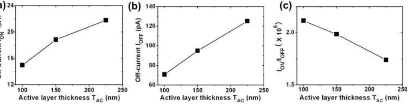
Figure 5 (a) - (c) show the relationships of on-current, ION, off-current, IOFF, and
on/off-current ratio, ION/IOFF, with different active layer thicknesses. ION and IOFF show the
same trend, that is: ION and IOFF both increase with the active layer thickness, TAC. The ION
increases with TAC due to the better crystalline quality. In addition, IOFF increases with the
active layer thickness TAC; indeed, when increasing TAC, a greater part of the active layer is
not under gate control and thus results in a higher leakage. Figure 5 (c) shows that reducing
between ION and IOFF variations with different active layer thicknesses TAC.
Due to the in-situ doping during the LPCVD process, P-type and N-type VTFTs could be
easily fabricated in the same run, just by adopting different dopant gases (PH3 or B2H6) for
source and drain regions. For such VTFTs, the 150 nm thick active layer is chosen,
corresponding to a good compromise between the ION/IOFF ratio and the mobility µFE.
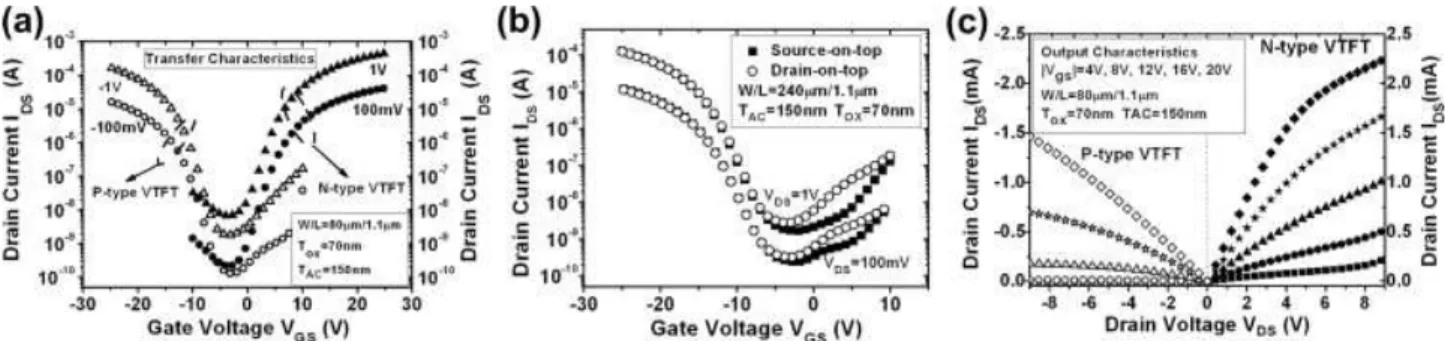
The typical transfer characteristics of the P-type and N-type VTFTs are shown in figure 6
(a), with the same W/L = 80 µm/1.1 µm. ION/IOFF ratios slightly higher than 105 are obtained
for both P and N-type VTFTs. For VDS = 100 mV, the deduced electrical parameters are listed
in table 2. The same subthreshold slope S of 1.9 V/dec is obtained for both P and N-type
VTFTs. For P-type VTFT, the field effect mobility µFE is 4.2 cm2/V·s, while the threshold
voltage VTH equals to -15 V. In contrast, for N-type VTFT, µFE is 7.5 cm2/V·s, while VTH
equals to 9.8 V. The difference of threshold voltage VTH between P-type and N-type VTFTs is
consistent with the polycrystalline silicon lateral counterparts [13]. Nevertheless, the two
types of VTFTs have shown symmetric ION and IOFF, which demonstrates the feasibility for
CMOS-like VTFT circuit applications as inverters or oscillators.
Figure 6 (b) shows the similar transfer characteristics of the source-on-top (SOT) and the
drain-on-top (DOT), which indicates that the source and drain electrodes could be permuted.
Figure 6 (c) shows the output characteristics of the fabricated VTFTs, the kink effect prevents
the saturation of the drain current, which could be suppressed by increasing the channel
length and thus undoped polycrystalline silicon thickness [14], and by improving the
crystalline quality of the active layer on the sidewalls.
of different dimensions. The same relationships have been obtained for the two types of
vertical TFTs, therefore, the relationships for P-type vertical TFTs are shown as an example.
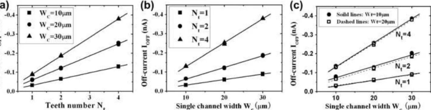
For ION, its relationships with different geometrical parameters are shown in figure 7. From
figure 7, ION shows a linear relationship with the tooth number, Nt, as ION is directly related
with the channel numbers (there are two channels for each tooth). In the first analyses, ION
appears independent of the gate width, WC. This behavior should means that a dependence of
ION with WC could be observed by decreasing the size, but a specific study must be made in
this case, especially by improving the design rule.
Figure 8 gives the relationships between the off-current IOFF and the geometrical
parameters. From figure 8 (a) and 8 (b), IOFF shows strictly linear relationships with the tooth
number Nt as well as the single channel width Wc, which confirm that the off-current IOFF is
directly related with the active layer region. From figure 8 (c), IOFF is independent of the tooth
width Wt, which highlights that IOFF is just brought by the active layer part between source
and drain, while the active layer on top of the tooth doesn’t have any effect on IOFF.
By combining the analysis of on-current ION and off-current IOFF, we can conclude that,
for a fixed tooth width Wt, the ION/IOFF ratio follows the equation:
1 ( .1) ON OFF t t c c I N eq I ∝ N W ∝W
Which means that for the vertical TFTs, the ION/IOFF ratio can be increased by reducing the
single channel width Wc, thus a narrow single channel width Wc is required, which is
approximate to the design rule. This also indicates a reduction of tooth length, which is fixed
In contrast, the tooth number, Nt, doesn’t affect the final ION/IOFF ratio, as expected, even
though the higher tooth number, Nt, enables to provide a higher ION, which is the major
advantage of our vertical TFTs. In addition, the ION/IOFF ratio is not affected by the tooth
width, Wt.
Dynamic characterizations of vertical TFTs were not performed, at this level of the study. It is
clear that in the first designs, the frequency parameters were not optimized; indeed, the
relatively large area of the source and drain coverage could lead to a high parasitic capacitance
and decrease the frequency performances. However, this source to drain parasitic capacitance
effect is lowered since we used a 1 µm thick undoped polysilicon layer deposited on the SiO2
thin film, which increases the channel length as well as the equivalent insulating film thickness;
thus it decreases this parasitic capacitance. In addition, for the tooth width, a stabilized
industrial process should adopt the smallest distance compatible with the design rule. The area
of the capacitance should be minimized in this case.
5. CONCLUSION
This paper presents a vertical TFT structure fabricated by a low-temperature process
(T ≤ 600°C) polysilicon technology. By adopting the multi-gate structure, the total channel
width can be enlarged while the channel length can be very short for a vertical structure. The
electrical results show an ION/IOFF ratio of more than 105 with a field effect mobility µFE
around 10 cm2/V·s for different active layer thicknesses. P-type and N-type VTFTs have been
CMOS-like applications. The relationships of the electrical characteristics and the geometric
parameters have also been analyzed, the off-current IOFF is proportional to the tooth number,
Nt, and the single channel width, Wc, while the on-current, ION is only proportional to Nt. This
indicates that ION/IOFF ratio could be enlarged by adopting a smaller WC that approximates to
the design rule, which needs a modification of the masks. In addition, the field effect mobility
µFE could be increased by reducing the sidewall roughness and improving the crystalline
quality of the active layer.
ACKNOWLEDGEMENTS
The authors thank all the members of the department of microelectronics and
microsensors for their technological support on the fabrication process and for their kind
discussion. The authors also would like to thank Dr Joseph Lelannic for providing the SEM
References
[1] G. Beaucarne, S. Bourdais, A. Slaoui, J. Poortmans, Thin Solid Films 2002: 403–404:
229-237.
[2] Jin-Woo Han, Seong-Wan Ryu, Dong-Hyun Kim, and Yang-Kyu Choi, IEEE Trans.
Electron Dev. 2010: 57: 601–607.
[3] J.P. Lu, K. Van Schuylenbergh, J. Ho, Y. Wang, J.B. Boyce, and R.A. Street, Appl. Phys.
Lett. 2002: 80: 4656–4658.
[4] Satoshi Inoue, Sumio Utsunomiya, Takayuki Saeki, and Tatsuya Shimoda, IEEE Trans.
Electron Dev 2002: 49: 1353–1360.
[5] KeeChan Park, Jae-Hong Jeon, YoungIl Kimc, Jae Beom Choi, Young-Jin Chang, ZhiFeng
Zhan, ChiWoo Kim, Solid State Electron 2008: 52: 1691–1693.
[6] Tiemin Zhao, Min Cao, Krishna C. Sarawat, and James D. Flummer, IEEE Electron Dev.
Lett: 1994: 15: 415–417.
[7] Chao Sung Lai, Chung Len Lee, Tan Fu Lei, Horng Nan Chern, IEEE Electron Dev. Lett:
1996:17: 199-201.
[8] Ming-Zhen LEE, Chung-Len LEE and Tan-Fu Lei, Jpn J. Appl. Phys. 2003: 42:
2123–2126.
[9] P. Zhang, E. Jacques, R. Rogel, N. Coulon, O. Bonnaud, Solid State Electron 2013: 79:
26–30.
[10] P. Joubert, B. Loisel, Y. Chouan, and L. Haji, J. Electrochem. Soc. 1987: 134: 2541-2545.
[11] L. Pichon, K. Mourgues, F. Raoult, T. Mohammed-Brahim, K. Kis-Sion, D. Briand, and
[12] N.C.C. Lu, C.Y. Lu, M.K. Lee, C.C. Shih, C.S. Wang, W. Reuter, and T.T. Sheng, J.
Electrochem. Soc. 1984: 131: 897-902.
[13] Gael Gautier, Carlos Eduardo Viana, Samuel Crand, Regis Rogel, Nilton Itiro Morinioto,
and Olivier Bonnaud, Fourth IEEE International Caracas Conference on Devices,
Circuits and Systems: 2002 Aruba: DO14 –1-6.
[14] A. Valletta, P. Gaucci, L. Mariucci, G. Fortunato, S.D. Brotherton, Appl. Phys. Lett., 85
Figure captions
Figure 1: (a) 3D schematic of the VTFT structure, and (b) cross-sectional view of a tooth
structure. The 3D view shows multi gates. The tooth structure shows that the source and drain
electrical path is blocked by an insulating barrier, while the active layer is deposited after the
Figure 2: SEM of the optimized sidewall profile, which enables the active layer, the gate
oxide layer, and the Al layer depositions on it. It remains, however, a small recess at the level
of the SiO2 insulating layer due to the etching selectivity difference.
Figure 3: (a) SEM top view and (b) schematic side view of the fabricated vertical TFT.
The geometrical parameters, including the tooth number, Nt, the single channel width, Wc, and
Figure 4: Transfer characteristics for different active layer thicknesses TAC (225 nm, 150
nm, and 100 nm), ION/IOFF ratios higher than 105 are obtained.
Figure 5: (a) On-current ION, (b) off-current IOFF, and (c) ION/IOFF relationships with
different active layer thicknesses TAC. ION and IOFF increases with TAC, while ION/IOFF reduces
Figure 6: (a) Transfer characteristics of the P-type and N-type VTFTs, (b) transfer
characteristics for source-on-top (SOT) and drain-on-top (DOT) structure, and (c) output
characteristics of the P and N-type vertical TFTs. For the two types of VTFTs, the transfer
characteristics are symmetric. Source and drain can be permuted. Output characteristics are
affected by kink effect, which is due to the short channel length L.
Figure 7: Variation of ION with the tooth number: ION is proportional to the tooth number,
Figure 8: The relationships of IOFF with different geometrical parameters: (a) IOFF is
proportional to the tooth number, Nt, (b) IOFF is proportional to the single channel width, Wc,
and (c) IOFF is independent of the tooth width, Wt.
Active layer thickness (nm) S (V/dec) gm (µS) VTH (V) µFE (cm2/V s) ION/IOFF
225 1.3 1.2 3.9 13.2 1.74 × 10⁵ 150 1.3 1.0 4.4 11.5 1.98 × 10⁵ 100 1.2 0.8 5 9.2 2.11 × 10⁵
Table 1: Electrical parameters of VTFTs with different active layer thicknesses TAC. When
increasing TAC, threshold voltage VTH reduces and field effect mobility µFE increases, while
ION/IOFF ratio reduces.
VTFT type S (V/dec) VTH (V) gm (µS) µFE (cm2/V s)
P-type 1.9 −15 1.5 4.2 N-type 1.9 9.8 2.7 7.5