Abstract—In a flip chip package, the chip corner areas which are embedded in the underfill material are often critical to the damage initiation, since a stress concentration usually exists at these locations. A high level of stress concentration often promotes crack initiation from the chip corner. In order to better understand the local deformation around chip corners and crack tips, a method based on laser scanning confocal microscopy combined with the digital image correlation (confocal-DIC) was developed to measure local strain directly in deformed, transparent objects. A transparent epoxy resin with alumina particle fillers was used in four different types of samples, which were fabricated for the purpose of validation. A non-constrained sample and a thin-layer sample were used to verify the isotropic thermal expansion and the strain gradients with respect to the depth, respectively. Results from both samples were in good agreements with the calculation from the coefficient of thermal expansion (CTE) and FEM simulations. Furthermore, the confocal-DIC technique was applied to measure the strain distribution near the chip corner area of a third sample replicating the geometry of a flip chip package. The measured maximum first principal strain was located at the chip corner, reaching 0.9 % at 60 °C, in a good agreement with the simulation results. The strain in front of the crack tip was also evaluated by a three-point bending test in a fourth test sample. The measured maximum strain was 5.8±0.7 %, corresponding to a relative error of only about 5 % compared to simulations for a round crack tip configuration. The averaging used in DIC lowers its spatial resolution and makes it difficult to capture higher strain gradients in small regions. However, the confocal-DIC approach appears to be able to provide reasonable results for evaluating the maximum strain and the full field strain distribution in tri-dimensional volumes with geometries, materials and dimensions which are very similar to those of actual flip chip microelectronic packages.
Index Terms—Underfill, confocal microscopy, digital image correlation, deformation
I. INTRODUCTION
igh performance polymers and polymer-based composites are widely used in microelectronic packaging to enhance the reliability of the devices. An appropriate management of
Manuscript received July 9, 2019. This project was supported by the NSERC/IBM Collaborative Research and Development Grant in Numerical Modeling for Advanced Packaging.
The authors are with the Institut Interdisciplinaire d’Innovation Technologique (3IT), Université de Sherbrooke, Sherbrooke, Canada (e-mail: [email protected]).
stress and strain in microelectronic packaging is quite important, as the high level of stress often induces mechanical or electrical failures [1]. In flip-chip packages, the large mismatch in the coefficient of thermal expansion (CTE) between the silicon die and the organic substrate induces high stress levels, which are exacerbated by concentrations at interfaces and die corners, from which the underfill damage often originates [2]. Many of the reliability failures in flip-chip packages result from delaminations or cracks in the underfill material, which is applied between the die and the substrate to alleviate the effect of the aforementioned CTE mismatches on the solder joints [3]. Several types of underfill failure modes, such as the interface delamination and cracking, are observed in accelerated temperature cycling tests [4-5]. The cracks in the underfill may not initially cause an electrical failure, but may propagate over time into the solder joints and the die back end of line (BEOL), thus resulting in device failure [6]. Macroscopic fracture properties, such as the fracture toughness, adhesion strength and the critical energy release rate at the Si/polymer interface, can be experimentally measured, e.g. via the cantilever beam test [7-9]. Although these fracture properties can be applied as input parameters to models to evaluate the reliability of the package, it is still challenging to predict the lifetime of the devices due to the difficulties involved in estimating correctly the local stress or strain levels at some critical positions, such as the die corner, the solder joints and the BEOL.
Numerical simulations, such as those based on the finite element method, are a popular way to predict the stress levels at critical locations within the package [10-12]. Reference [13] has studied the singularity of the right angle geometry of the chip corner using two-dimensional fracture mechanics. In the case of quasi-static loading, the order of the singularity is only dependent on the elasticity constants of the two materials. Reference [14] has evaluated the interface shear stress considering the height and width of the underfill fillet, using the finite element method. In the experimental validations, no failures were observed to 3000 cycles (0 °C to 100 °C, ~2 cycles per hour), with fillet heights at the die corner varied from ~2 % to ~70 % of the die thickness. The microelectronic packaging Copyright © 2017 IEEE. Personal use of this material is permitted. However, permission to use this material for any other purposes must be obtained by sending a request to [email protected]
Using Confocal Microscopy and Digital Image
Correlation to Measure Local Strains Around a
Chip Corner and a Crack Front
Ying Yang, Papa Momar Souare, and Julien Sylvestre
community relies on numerical simulations to predict stresses and strains that develop within package structures. However, numerical models do not always provide enough accuracy due to approximations on geometries, materials properties, etc. Considering the chip dicing process, the real die corner is not a perfect cube and its geometry is hard to model precisely. The dicing might provide a rough surface on the sidewalls, and the chip faces might not form a perfect 90° right angle [15,16]. In addition, the underfill usually consists of inorganic particle fillers added to a resin to improve its mechanical properties. Due to the variability of filler sizes, contents and curing process, the underfill is not perfectly uniform on a scale of a few tens of micrometers, and may exhibit the separation of fillers and resin [17] and cavities [7]. The finite element method itself also has limitations on calculating the stress at the singularity point, with results that are not convergent when reducing the element size [18]. The above restrictions remain a significant obstacle to obtaining the correct stress and strain value near the chip corner, thus increasing the difficulty of fatigue predictions.
Direct measurements of strain in the underfill would be useful to validate existing physical models or to develop new models to improve the accuracy of numerical simulations. The local deformation of the underfill around the die corner is challenging to measure experimentally, since the relevant area is small (< 1 mm3) and the pyramid corner is totally hidden inside the underfill and is not directly accessible. Several experimental techniques have been proposed to measure the strain at small scales in the underfill. Carbon nanotubes (CNTs) can be a good strain sensor, because their Raman shift responds linearly to imposed strains [19-21]. Reference [22] has dispersed single-wall carbon nanotubes (SWCNTs) in the underfill to measure the internal strains. However, this approach as presented works only in two dimensions, and the position of the measured maximum strain appeared to be quite random and not located at the chip corner, thus raising questions about the validity of the method. Other 2-dimensional methods, such as moire interferometry and conventional digital image correlation, can only provide deformations on the exterior surface of the underfill [23-25]. Scanning acoustic microscopy is able to detect the voids and delaminations inside the underfill, but does not have sufficient resolution to provide information about strains [26-28]. In order to obtain the global distribution of strains inside an assembly, displacements in three dimensions must be estimated. Unlike 2-dimensional strain mapping, the 3-dimensional microscale strain field is more difficult to obtain by strain sensors or conventional optical microscopy. An X-ray micro-computed tomography (Micro-CT) has been applied in 3-D reconstruction on metallic components, while the digital volume correlation method (DVC) was used to calculate their volumic deformations [29-31]. However, due to the rotational scanning configuration of the micro-CT, the spatial resolution is limited by the size of the assembly, which makes it difficult to realize high-resolution imaging on a large sample. As an example, the typical voxel sensitivity of micro-CT in reference [29] is 157 157 157 µm3 for a silicone soft material sample with a dimension of 20 10 3 mm3. References [32,33] describe an optical scanning
tomography method to obtain 3D images by using a laser plane, with a spatial resolution reaching 60 60 60 µm3 per voxel. Due to their limited spatial resolution, these methods are not appropriate to capture the deformation gradient in the underfill precisely, especially near the chip corner area and in front of the possible cracks.
Laser scanning confocal microscopy (LSCM) avoids some of the drawbacks of other 3D methods, as it scans the sample from one side by controlling the position of the focal plane and can provide high resolution images of volumes. Reference [34] has combined the LSCM and DVC methods to mesure large strains (up to 25 %) in agarose gels (with typical sample dimensions of 6.4 mm in diameter and 1.4 mm in height). The DVC requires well-structured voxels, while the underfill is a fairly thin layer (tens of micrometers). According to the geometry of voxels used in reference [32-34], only one or two voxels could be constructed along the layer thickness in an underfill layer, which would translate into a low vertical resolution. Conventional 2-dimensional DIC is simpler to apply on such thin layers, by choosing enough slices when the sample warpage is negligible.
In this paper, we report on the development of an experimental approach to measure the local strain distribution inside a quasi-transparent material for the geometry of a flip-chip corner and a sample with a prefabricated crack. LSCM is combined with digital image correlation (DIC) to produce a method (confocal-DIC) which was used for strain measurements with excellent strain sensitivity (~0.01 %) and spatial resolution (37 37 3 µm3) in a small volume (1200 1200 60 µm3). Section 2 presents the procedure for sample preparation and the measurement protocol. Section 3 provides the details of finite element models used to confront the experimental results. The results of the comparison to the models and applications of the confocal-DIC method are discussed in section 4.
II. EXPERIMENTS
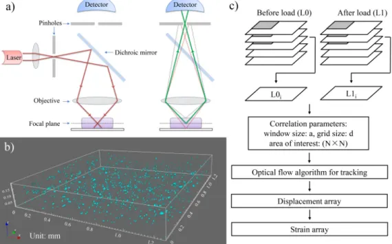
In order to realize the characterization of local strain inside the materials, laser scanning confocal microscopy was applied in this study. Conventional optical microscopes collect visible light from a large fraction of the sample volume, and cannot separate the image at the focal plane from images at other out-of-focus planes. However, the LSCM uses a pinhole in front of the detector to block the incoming light from the volume outside of a thin focal plane region. Fig. 1a shows the general principle of the LSCM, including the step of illuminating (left) and light collection (right). During the illuminating step, the laser is reflected by the dichroic mirror and focused on the sample. Then, the reflected lights goes through the dichroic mirror and is directed toward the detector. Due to the finite focal depth of the objective lens and the angular selection of light rays by the pinhole, only the light from a shallow region around the focal plane can reach the detector. By controlling the vertical position of the sample, a series of sliced images can be produced and stacked vertically. Fig. 1b displays a typical stacked image
obtained by the LSCM (Olympus FV3000, laser at 640 nm wavelength, 10 UPlanSApo objective), with particle fillers dispersed in the epoxy resin as position markers (fabrication details below).
The image processing procedure used to obtain a estimate of planar strain in each slice of the stacked image is shown in Fig. 1c. After obtaining two stacks of images, before (L0) and after
(L1) applying the load, the same layer in each stack is selected and the calculation parameters are initialized. Then, the 2D displacement array is obtained by comparing the images from the two stacks using a digital image correlation algorithm, and the strain values are finally calculated from the displacement array. Herein, this technique, which combines the features of confocal microscopy and digital image correlation method, is called the confocal-DIC method.
Fig. 1. (a) General principle of the laser scanning confocal microscopy; left: incident laser illuminating the sample, right: pinhole accepting the reflection from the focal plane, thus rejecting most out-of-focus light. (b) Typical 3-dimentional stacked image, with particle fillers dispersed in epoxy resin. (c) Diagram of the image processing.
The underfill material used in this work was composed of the SU-8 2005 epoxy resin, which was loaded with particle fillers consisting of alumina powder (1 µm in diameter). The SU-8 2005 epoxy is thermally and chemically stable and it has an excellent optical transparency when the light wavelengh is above 500 nm [35]. The nominal Young's modulus and coefficient of thermal expansion of unloaded SU-8 2005 are 2 GPa and 52∙10-6/°C, respectively [36]. Before curing the epoxy, about 0.1 wt% alumina particle fillers were ultrasonically dispersed in the epoxy to ensure a good distribution of the particles as position markers. The concentration of fillers should be low to avoid the occlusion of fillers by other fillers above, and to avoid modifying the mechanical properties of the epoxy too much. It must however be appropriately high to allow an accurate strain calculation during the image processing.
Four types of specimens were prepared as illustrated in Fig. 2. The first sample was used to validate the thermal expansion deformation. The mixed resin and fillers were formed on a silicone substrate, so it could be removed from the substrate easily (c.f. Fig. 2a). It was placed on the microscope stage directly, without any boundary limitations. The second sample was designed to verify the capability of the method to characterize the strain gradient along the thickness of the sample. The epoxy mixture was coated on a transparent glass
substrate, with a thickness that was carefully controlled at 0.1 mm by grinding and polishing (c.f. Fig. 2b). Both of these two samples were imaged at 24 °C, 36 °C, 48 °C and 60 °C, over a 1.2 1.2 mm2 area of interest. A thermocouple was also used to monitor the temperature on the sample, as the air convection usually caused heat dissipation on the surface.
The third sample in Fig. 2c was used to measure the deformation near the chip corner area. A rectangular silicon die was encapsulated on a glass substrate by the same epoxy mixture, so that it provided a right angle boundary to the epoxy. The epoxy mixture played a role similar to the underfill in a flip-chip package, with the fillet width chosen to be large (about 3 mm) to avoid the effects of the free surface. The sample was cured at 170 °C for 20 minutes and then cooled down slowly on a hotplate. This sample was imaged at 24 °C and 60 °C to obtain the local deformation near the chip corner (24 °C was used as the reference temperature).
The fourth sample in Fig. 2d was used to characterize the deformation near a crack tip, which had a greater strain concentration than the right angle geometry. For the purpose of having a perfect surface on the sample, a high temperature tape was placed inside a rectangular aluminum mould (20 10 2 mm3) during the epoxy curing. The aluminum mould was dissolved in a HCl solution and the tape was easily removed
manually. A pre-crack, 2 mm in length, was produced in the centre of the long edge by a sharp blade. Refering to the standard ASTM E1820 [37], the whole sample was loaded in a 3-point bending test fixture, and the displacement of the loading point (about 0.2 mm) was measured by an optical microscope.
Although the area near the indenter imposing the displacement at the loading point may present a large stress gradient, the crack position is far away enough from the indenter, the finite element simulations show that its influence on the stress distribution near the crack can be neglected.
Fig. 2. Diagrams of the samples preparation: (a) non-constrained sample, (b) thin-layer sample, (c) chip-corner sample and its cross-section view, (d) 3-point bending sample with a prefabricated crack.
As described in Fig. 1c, we obtained two series of stacked LSCM images from the same region in each sample (before loading and after loading). A global vertical alignment was accomplished by carefully comparing their patterns of speckles in order to choose the photos from the same vertical position. The pixel size in the LSCM images was 2.5 2.5 µm2. A Python-based DIC script was used with a correlation window (subtile) of 50 50 pixel2 and a grid size of 15 15 pixel2 [38]. The DIC script firstly tracked the displacement of each subtile (in two dimensions) and then calculated the strain component x, y and xy from the central difference of displacements in four grid points. After obtaining the displacement and strain array of each layer, the strain contours were stacked to form volumetric representations of the strain fields. Currently, we did not apply the DVC to calculate the full 3-dimensional deformation, but might develop it in the future.
III. MODELING
Of the four samples, only the deformation in the first non-constrained sample could be easily calculated analytically from the CTE due to the complexity of the geometries. Thus, the finite element method was used to compare the results between the experiments and theoretical expectations, for the last three samples. The finite element models are shown in Fig. 3, using the same geometry as the samples and material properties as
described in Table I. As is common practice in this field, the mechanical properties of silicon were simplified as isotropic, since the Young’s modulus of the underfill is significantly lower than the modulus of the silicon, so the anisotropic nature of silicon has only a small influence on the deformation of underfill. As mentioned in the reference [39], the crystal structure of silicon has cubic symmetry, so calculations for devices with orthogonal shapes and loads will be reasonably accurate. Several researchers [40,41] also chose one single elasticity value for the silicon die. As the loading temperatures did not exceed 60 °C, only the material properties of the underfill under the Tg were used. To create the parametric numerical models efficiently, a custom software was used, PACK [42] . PACK is a Python-based high performance numerical software, incorporating advanced pre- and post-processing features for multiple commercial finite element softwares (including Ansys APDL used in this work) [43]. The chip-corner models were generated by PACK (c.f. Fig. 3b), with two sizes of underfill elements (40 µm and 24 µm) used to study how to best capture the corner strain concentration. A quarter simplification was used for the thin-layer model and chip-corner model, while a x-symmetric and y-symmetric boundary condition were applied on the yz and xz plane. A fixed constraint was also applied on the node at (0,0,0) to avoid rigid body motion. In order to correctly calculate the deformation, the reference temperature was set at 24 °C, in accordance with the experimental measurements. In the 3-point
bending model (c.f. Fig. 3c), two types of crack front (round and triangular) were also used, since the real crack front produced by the blade is possibly between these two ideal geometries.
TABLE I
MATERIAL PROPERTIES IN MODELS
Die Underfill Substrate
Young’s Modulus (GPa) 120 2 (below Tg) 0.5 (above Tg) 82 CTE (10-6 /°C) 2.6 52 (below Tg) 298 (above Tg) 7.1 Tg (°C) 210 Poisson ratio 0.35 0.3 0.2
Fig. 3. Finite element models of the (a) thin-layer sample, (b) chip-corner sample, (c) 3-point bending sample, with a round and a triangular crack front geometry.
In Fig. 3a and 3b, we used 8-node solid elements for most
components, while the underfill fillet was modeled by prisms and tetrahedral elements due to the complex geometry. Parabolic 20-node solid elements were used to build the crack models for more accurate strain evaluation near the crack tip. Uniform temperatures were applied on the thin-layer and chip-corner models. A 0.2 mm central displacement load was set on the the 3-point bending sample. All the FEM models were solved by the Ansys Sparse solver. We extracted the deformation on the edge of the thin-layer model, the strains along the diagonal direction from the chip corner and along the vertical direction from the crack tip.
IV. RESULTS AND DISCUSSION
The aim of the non-constrained sample and the thin-layer sample was to validate the feasibility of the confocal-DIC method. The shape of the non-constrained sample was entirely defined by the effect of fluid surface tension. This sample was free of restriction on its boundary, so that the strain εi at each position was controlled by the CTE α of the bulk material and is expressed by
i
T
(1) where ΔT is the temperature difference between the two load conditions, and ix,y,xy indicates the components of strain. As described in Fig. 4a, both the strain components x and y were evaluated by the confocal-DIC method. Each measured point in Fig. 4a represents the average value and standard deviation calculated over the strain components in a 9-slice stacked image. The measured deformation for components x and y showed a quasi-linear relationship with respect to the temperature of the sample, with a slope comparable to the CTE of the epoxy. The average strains of both the x and y components were in good agreement with the calculations from the CTE at each test temperature, with the maximum relative error reaching 13.5 % for the strain component y at 54.6 °C. The averaged strain values obtained by a linear fit gave a CTE of (47.2±4.5)10 -6/°C, slightly lower but consistent with the SU-8 2005 expected value of 52.010-6/°C. Fig. 4b shows typical images of εx, εy and εxy for one layer. εx and εy increased with temperature, while εxy was small and independent of temperature.
Fig. 4. (a) Strain components x (dashed line), y (dotted line) and xy (dot-dash line) in the non-constrained sample and the strain calculated from the CTE (solid line), with respect to loading temperatures. Error bars represent one standard deviation. (b) Typical strain images for one layer at 33.6 °C, 43.4 °C and 54.6 °C.
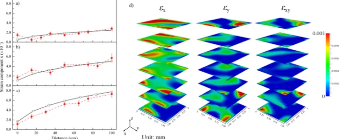
The thin-layer sample was used to verify the measurement of strain gradients with respect to the depth inside the material. Since the glass substrate had a low CTE and a high Young’s modulus, the deformation of the epoxy mixture near the bi-material interface was strongly controlled by the glass substrate. Thus, an increase of deformation is expected along a path from the interface to the free edge. Fig. 5 summarizes the results for strain component x. With increasing temperatures, the strain gradients became more significant in both simulations and experiments. Due to image noises compared to the small
deformation, some data fluctuations are clearly visible, especially near the interface area. However, the global trends of these strain values were in a good agreement with the simulation results. The maximum strain on the component x reached 2.8∙10-4, 5.7∙10-4 and 7.3∙10-4 at the three measurement temperatures, which shows a good sensitivity for small deformation measurements. Fig. 5d presents typical strain images of εx, εy and εxy at 54.6 °C. Although some noise is clearly present, an εx can still be observed to be increasing along the z direction, while εy and εxy keep a relatively low level.
Fig. 5. Strain component x of the calculation (solid line) and the measurement (dashed line) with respect to vertical distance from the bi-material interface in the thin-layer sample at (a) 33.6 °C, (b) 43.4 °C and (c) 54.6 °C. Error bars represent one standard deviation. (d) Typical strain images at 54.6 °C.
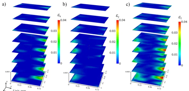
The above two preliminary validation tests show that the confocal-DIC method is capable to measure local deformations at the micrometer scale and to produce reasonable strain estimates. We next apply this method to evaluate the underfill deformation near the chip corner area, as described in Fig. 2c. Fig. 6 shows the measured first principal strain in the underfill, with the chip area shown in grey (without considering its deformation). The vertical step (gap between two slices in the image stack) for all the four samples was set as 3 µm in order to collect enough information and avoid missing possibly large strain gradients. The 1st to 4th layers from the top represent the area above the chip corner and the 6th to 9th layers were the underfill between the chip and the substrate. The 5th layer from the top was exactly the layer at the corner point. The maximum value of the first principal strain appears at the chip corner area in the 5th layer and reaches 0.9 %. On the edge of the sidewall, the maximum value reaches about 0.5 %. Although the first principal strains on the 1st to 4th layer were generally lower than on the 5th layer, the in-plane maximum value was still located near the chip corner and the interface regions. From 6th to 9th layers, a broad area reaches 0.5 % deformation as a result of the differences of CTE between the silicon die and glass substrate.
Fig. 6. 3-dimensional stacked images of the first principal strain near the chip corner at 60 °C.
In order to further compare the effect of strain concentration between the simulations and experiments, Fig. 7 shows the first principal strain along the diagonal direction from the chip corner. Considering the singularity effect on the right angle area, the strain concentration was steeper in simulation results than in experiments. Smaller elements were also better able to capture the local strain gradient. The maximum strain in the model with 24 µm and 40 µm elements sizes reached 1.16 %
and 1.10 % respectively, while the measured maximum strain was 0.92 %. The measured value was about 20 % lower than the simulation, since the real chip corner was not a perfect pyramid (e.g. due to imperfect dicing of the die). When the position is 50 µm away from the strain concentration area, all the three values remain at a similar, low strain level (0.1-0.2 %).
Fig. 7. First principal strain at 60 °C as a function of the distance from the chip corner in the diagonal direction, for the calculation with an element size of 24 μm (dashed line) and 40 μm (dotted line), and the measurements (triangle markers) with an exponential fitting curve (solid line). Error bars represent one standard deviation.
As the chip corner is often subjected to high strain levels, many reliability tests have found that cracks might initiate from the chip corner and then propagate into the underfill and the back end of line (BEOL). Thus, we have also tried to characterize the strain distribution in front of a single crack by the 3-point bending test, as described in Fig. 2d. The central displacement load was 0.2 mm, measured by an optical microscope. Fig. 8 shows the measured strain contours near the crack front area on the component x, y and the first principal strain. Since the central load was along the y direction, the mode I crack was dominant, which means that the tensile stress was normal to the crack plane yz. The strain component x (Fig. 8a) showed a significant concentration near the crack front area (the right edge of images), while the strain component y (Fig. 8b) was generally low, indicating the same situation of mode I crack. Here we still use the first principal strain to evaluate the global strain level in the crack front area (Fig. 8c). A high level of strain concentration can be observed from the right edge of the images.
Fig. 8. 3-dimensional stacked images of the (a) strain component x, (b) strain component y, (c) first principal strain in front of the crack area. In order to compare the results between the experiments and
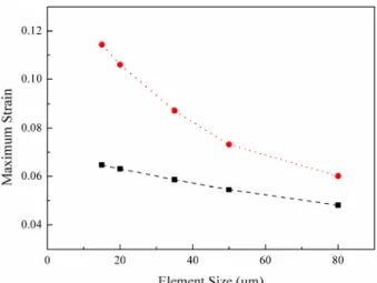
simulations, Fig. 9 summarizes the relationship between the maximum first principal strain and the element size for round and triangular crack tip configuration in the FEM simulation. Since the real crack tip is not a sharp angle but has a small radius, these two configurations were analyzed, representing two types of ideal geometry of the crack tip. Due to the singularity effect, the strain at the triangular crack tip increased rapidly and became non-convergent when the element size was less than 40 µm. However, the strain at the round crack tip was generally stable. Here we chose the results of the element size at 35 µm for further comparison with the experiments, to have a similar resolution as in the DIC calculation (37 37 µm2). Fig. 10 shows the first principal strains along the y direction from the
crack front. The triangular tip model had the highest strain level near the crack, reaching 9.2 %, while the maximum strain for the round tip model was 6.1 %. The experimental data were quite close to the round tip configuration at 5.8±0.7 %, only about 5 % lower than that in the round tip model. Since the DIC calculates a single strain value for each correlation window, strong deformation gradients near the crack tip are averaged, which is equivalent to a spatial low-pass filter in the data processing. This results in a smoothing of the strain distribution and reduces the slope in high strain gradient areas. Although it is difficult to capture high strain gradients by our method, it is still useful to evaluate the maximum strain level and the general distribution of full strain fields.
Fig. 9. Maximum first principal strain at the round crack tip (dashed line) and the triangular crack tip (dotted line) with respect to the element size.
Fig. 10. First principal strain along the crack front direction in the calculation with a round crack front (dashed line) and a triangular crack front (dotted line), and the measurements (diamond markers) with an exponential fitting curve (solid line). Error bars represent one standard deviation.
V. CONCLUSION
In this work, we have developed a methodology for measuring the local strain inside the underfill material directly. This technique combines the advantages of the laser scanning confocal microscopy and digitial image correlation methods, and is able to provide a 3-dimensional stacked strain contours. Four types of samples were fabricated for the purpose of validation. A preliminary validation was performed by a non-constrained sample and a thin-layer sample, for the thermal expansion deformation and the strain gradient with respect to the depth in the material. Both the strain components x and y in the non-constrained sample were in a good agreement with the coefficient of thermal expansion (CTE) of the bulk resin. The strain gradients obtained in the thin-layer sample were consistent with the simulation results, as a function of the depth from the resin/glass interface. This demonstrates the usefulness of the confocal-DIC approach in obtaining the internal strain of quasi-transparent materials at the micrometer scale. We applied this approach to measure the strain in the underfill around a chip corner. The first principal strain reached 0.9 % at the corner area,
which is close to the simulation results. In the 3-point bending test, a higher strain concentration was found in front of the crack tip, while the measured maximum strain was 5.8±0.7 %, only about 5 % lower than the simulations of the round crack tip configuration.
The confocal-DIC approach seems to have some difficulties to capture very high strain gradients, because of the limitations on resolution and the averaging effect in each correlation window resulting from the DIC calculation. It can nevertheless provide very reasonable results for evaluating the maximum strain and the full field strain distribution in a 3-dimensional stacked view. It is expected that this technique will provide more opportunities to understand the real microscale mechanical behaviour inside materials, thus leading to better reliability estimates for microelectronic devices.
ACKNOWLEDGMENT
The authors thank Daniel Garneau from University of Sherbrooke for the support of the confocal microscope.
REFERENCES
[1] I. Nnebe, S. Park, and C. Feger, “Direct measurement of local stress in first-level flip-chip organic packages,” In Proc. 60th Electron. Comp. Technol. Conf., June 2010, pp. 1266-1272.
[2] M. C. Paquet, J. Sylvestre, E. Gros, and N. Boyer, “Underfill delamination to chip sidewall in advanced flip chip packages,” In Proc. 59th Electron. Comp. Technol. Conf., May 2009, pp. 960-965.
[3] Z. Zhang, and C. P. Wong, “Recent advances in flip-chip underfill: materials, process, and reliability,” IEEE Trans. Adv. Packag., vol. 27, no. 3, pp. 515-524, 2004.
[4] T. Sinha, T. J. Davis, T. E. Lombardi, and J. T. Coffin, “A systematic exploration of the failure mechanisms in underfilled flip-chip packages,” In Proc. 65th Electron. Comp. Technol. Conf., May 2015, pp. 1509-1517. [5] M. C. Paquet, C. Dufort, T. E. Lombardi, T. Sinha, M. Hasegawa, K. Okoshi, and K. Kohara, “Effect of underfill formulation on large-die, flip-chip organic package reliability: a systematic study on compositional and assembly process variations,” In Proc. 65th Electron. Comp. Technol. Conf., May 2016, pp. 729-736.
[6] C. J. Zhai, U. Ozkan, A. Dubey, R. C. Blish, and R. N. Master, “Investigation of Cu/low-k film delamination in flip chip packages,” In Proc. 56th Electron. Comp. Technol. Conf., May 2006, pp. 709-717. [7] M. C. Paquet, M. Gaynes, E. Duchesne, D. Questad, L. Bélanger, and J.
Sylvestre, “Underfill selection strategy for Pb-free, low-K and fine pitch organic flip chip applications,” In Proc. 56th Electron. Comp. Technol. Conf., May 2006, pp. 1595-1603.
[8] M. D. Diop, M. C. Paquet, D. Danovitch, and D. Drouin, “Void-free underfill process with variable frequency microwave for higher throughput in large flip chip package application,” IEEE Trans. Device Mater. Rel., vol. 15, no. 2, pp. 250-257, 2015.
[9] X. Fan, J. Zhou, and A. Chandra, “Package structural integrity analysis considering moisture,” In Proc. 58th Electron. Comp. Technol. Conf., May 2008, pp. 1054-1066.
[10] X. J. Fan, H. B. Wang, and T. B. Lim, “Investigation of the underfill delamination and cracking in flip-chip modules under temperature cyclic loading,” IEEE Trans. Comp. Packag. Technol., vol. 24, no. 1, pp. 84-91, 2001.
[11] C. J. Zhai, R. C. Blish, and R. N. Master, “Investigation and minimization of underfill delamination in flip chip packages,” IEEE Trans. Device Mater. Rel., vol. 4, no. 1, pp. 86-91, 2004.
[12] A. Q. Xu, and H. F. Nied, “Finite element analysis of stress singularities in attached flip chip packages,” J. Electron. Packag., vol. 122, no. 4, pp. 301-305, 2000.
[13] J. C. W. Van Vroonhoven, “Effects of adhesion and delamination on stress singularities in plastic-packaged integrated circuits,” J. Electron. Packag., vol. 115, no. 1, pp. 28-33, 1993.
[14] K. Kacker, S. Sidharth, A. Dubey, C. J. Zhai, and R. C. Blish, “Impact of underfill fillet geometry on interfacial delamination in organic flip chip
packages,” In Proc. 56th Electron. Comp. Technol. Conf., May 2006, pp. 1604-1610.
[15] Y. Fan, A. Arevalo, H. Li, and I. G. Foulds, “Low-cost silicon wafer dicing using a craft cutter,” Microsys. Technol., vol. 21, no. 7, pp. 1411-1414, 2015.
[16] M. Kumagai, N. Uchiyama, E. Ohmura, R. Sugiura, K. Atsumi, and K. Fukumitsu, “Advanced dicing technology for semiconductor wafer— stealth dicing,” IEEE Trans. Semicond. Manuf., vol. 20, no. 3, pp. 259-265, 2007.
[17] M. C. Paquet, D. Danovitch, P. M. Souare, and J. Sylvestre, “Study of capillary underfill filler separation in advanced flip chip packages,” In Proc. 67th Electron. Comp. Technol. Conf., May 2017, pp. 1361-1368. [18] S. S. Pageau, P. F. Joseph, and S. B. Biggers Jr, “Finite element analysis
of anisotropic materials with singular inplane stress fields,” Int. J. Solids Struc., vol. 32, no. 5, pp. 571-591, 1995.
[19] S. Yashiro, Y. Sakaida, Y. Shimamura, and Y. Inoue, “Evaluation of interfacial shear stress between multi-walled carbon nanotubes and epoxy based on strain distribution measurement using Raman spectroscopy,” Compos. Part A: Appl. Sci. Manufact., vol. 85, pp. 192-198, 2016. [20] C. A. Cooper, R. J. Young, and M. Halsall, “Investigation into the
deformation of carbon nanotubes and their composites through the use of Raman spectroscopy,” Compos. Part A: Appl. Sci. Manufact., vol. 32, no. 3-4, pp. 401-411, 2001.
[21] P. Dharap, Z. Li, S. Nagarajaiah, and E. V. Barrera, “Nanotube film based on single-wall carbon nanotubes for strain sensing,” Nanotechnology, vol. 15, no. 3, pp. 379-382, 2004.
[22] I. Nnebe, S. Park, and C. Feger, “Using single-wall carbon nanotubes and Raman spectroscopy to measure local stresses in first-level flip-chip organic packages,” IEEE Trans. Comp. Packag. Technol., vol. 1, no. 10, pp. 1601-1607, 2011.
[23] Y. Sun, and J. H. Pang, “Digital image correlation for solder joint fatigue reliability in microelectronics packages,” Microelectron. Reliab., vol. 48, no. 2, pp. 310-318, 2008.
[24] X. Q. Shi, Y. L. Zhang, and W. Zhou, “Determination of fracture toughness of underfill/chip interface with digital image speckle correlation technique,” IEEE Trans. Comp. Packag. Technol., vol. 30, no. 1, pp. 101-109, 2007
[25] D. Vogel, el al., “Stress analyses of high spatial resolution on TSV and BEoL structures,” Microelectron. Reliab., vol. 54, no. 9-10, pp. 1963-1968, 2014.
[26] S. Brand, P. Czurratis, P. Hoffrogge, and M. Petzold, “Automated inspection and classification of flip-chip-contacts using scanning acoustic microscopy,” Microelectron. Reliab., vol. 50, no. 9-11, pp. 1469-1473, 2010.
[27] G. M. Zhang, D. M. Harvey, and D. R. Braden, “Microelectronic package characterisation using scanning acoustic microscopy,” NDT & E Int., vol. 40, no. 8, pp. 609-617, 2007.
[28] W. J. Wolter, M. Speck, and R. Heinze, “Reliability analysis in microelectronic packaging by acoustic microscopy,” In Proc. 28th Int. Spring Seminar Electron. Technol., May 2005, pp. 436-443.
[29] P. Lall, and J. Wei, “X-ray micro-CT and DVC based analysis of strains in metallization of flexible electronics. In Proc. 16th IEEE Int. Conf. Thermal Thermomechan. Phenom. Electron. Syst., May 2017, pp. 1253-1261.
[30] K. Cinar, and I. Guven, “Micro-computed tomography as a tool to investigate the deformation behavior of particulate-filled composite materials,” J. Engin. Mater. Technol., vol. 140, no. 2, pp. 021001(1-18), 2018.
[31] P. Lall, and J. Wei, “X-ray micro-CT and digital-volume correlation based three-dimensional measurements of deformation and strain in operational electronics,” In Proc. 56th Electron. Comp. Technol. Conf., May 2015, pp. 406-416.
[32] A. Germaneau, P. Doumalin, and J. C. Dupré, “Comparison between X-ray micro-computed tomography and optical scanning tomography for full 3D strain measurement by digital volume correlation,” NDT & E Int., vol. 41, no. 6, pp. 407-415, 2008.
[33] A. Germaneau, P. Doumalin, and J. C. Dupré, “3D strain field measurement by correlation of volume images using scattered light: recording of images and choice of marks,” Strain, vol. 43, no. 3, pp. 207-218, 2007.
[34] C. Franck, S. Hong, S. A. Maskarinec, D. A. Tirrell, and G. Ravichandran, “Three-dimensional full-field measurements of large deformations in soft materials using confocal microscopy and digital volume correlation,” Exp. Mechan., vol. 47, no. 3, pp. 427-438, 2007.
[35] A. Del Campo, and C. Greiner, “SU-8: a photoresist for high-aspect-ratio and 3D submicron lithography,” J. Micromechan. Microengin., vol. 17, no. 6, pp. 81-95, 2007.
[36] Y. Pan, N. Khan, M. Lu, and J. Jeon, “Organic microelectromechanical relays for ultralow-power flexible transparent large-area electronics,” IEEE Trans. Electron Devices, vol. 63, no. 2, pp. 832-840, 2015. [37] Standard test method for measurement of fracture toughness. ASTM
E1820, 2011.
[38] https://gitlab.com/damien.andre/pydic/
[39] M. A. Hopcroft, W. D. Nix, and T. W. Kenny, “What is the Young's modulus of silicon?”. J. Microelectrom. Syst., vol. 19, no. 2, pp. 229-238, 2010.
[40] M. Y. Tsai, C. J. Hsu, and C. O. Wang, “Investigation of thermomechanical behaviors of flip chip BGA packages during manufacturing process and thermal cycling,” IEEE Trans. Comp. Packag. Technol., vol. 27, no. 3, pp. 568-576, 2004.
[41] L. Chen, Q. Zhang, G. Wang, X. Xie, and Z. Cheng, “The effects of underfill and its material models on thermomechanical behaviors of a flip chip package,” IEEE Trans. Adv. Packag., vol. 24, no. 1, pp. 17-24, 2001. [42] J. Sylvestre, “Integrated modeling of C4 interconnects,” In Proc. 57th
Electron. Comp. Technol. Conf., May 2007, pp. 1084-1090.
[43] M. K. Toure, P. M. Souare, S. Allard, B. Foisy, E. Duchesne, and J. Sylvestre, “CFD-based iterative methodology for modeling natural convection in microelectronic packages,” In Proc. 19th Int. Conf. Thermal Mechan. Multi-Phys. Simul. Exp. Microelectron. Microsyst., Apr. 2018, pp. 1-8.
Ying Yang received the B.Eng. degree and M.Eng.
degree from the Civil Aviation University of China, Tianjin, China, in 2014 and 2017, respectively.
He is currently pursuing the Ph.D. degree with the Université de Sherbrooke, Sherbrooke, Canada. His current research interests include the reliability of underfill and life prediction of the microelectronic packaging.
Papa Momar Souare received the diploma of
engineer in mechanical engineering from Ecole Polytechnique de Tours (France) in 2010. In 2011, he joined STMicroelectronics (Crolles, France), and worked as a Modeling Engineer in the Technology Modeling Team. He obtained his PhD degree from Ecole Nationale Supérieure des Mines de Saint-Étienne (France) in November 2014. Since 2015, he has been a research associate at the Université de Sherbrooke (Canada). His research interests include numerical modeling and thermal and mechanical issues in microelectronic packages.
Julien Sylvestre received the B.Sc. degree in
physics from McGill University (Montréal, Canada) in 1998, and the Ph.D. degree in physics from the Massachusetts Institute of Technology (Cambridge, USA) in 2002. He was a Post-Doctoral Scholar at the California Institute of Technology and at NASA's Jet Propulsion Laboratory (Pasadena, USA) until 2004, when he joined the IBM Corporation (Bromont, Canada), where he worked in microelectronics R&D as principal technical professional in the Systems and Technology Group. He joined the Université de Sherbrooke as an Associate Professor of Mechanical Engineering in 2014, where he currently is chairholder of the NSERC/IBM Canada Industrial Research Chair in High Performance Heterogeneous Integration. His research interests include many aspects of thermal and mechanical phenomena in microsystems, including numerical simulation methods, cooling, reliability, and the integration of advanced functionalities such as photonics and artificial intelligence.