O
pen
A
rchive
T
OULOUSE
A
rchive
O
uverte (
OATAO
)
OATAO is an open access repository that collects the work of Toulouse researchers and
makes it freely available over the web where possible.
This is an author-deposited version published in :
http://oatao.univ-toulouse.fr/
Eprints ID : 19301
To link to this article : DOI: 10.1109/TPS.2017.2777835
URL
http://dx.doi.org/10.1109/TPS.2017.2777835
To cite this version : Florez, David and Schitz, Dmitry and Piquet,
Hubert and Diez, Rafael TEfficiency of an Exciplex DBD Lamp
Excited Under Different Methods (2017), IEEE Transactions on
Plasma Science, vol. 46, n1, pp.140-147
Any correspondance concerning this service should be sent to the repository
administrator:
[email protected]
Efficiency of an Exciplex DBD Lamp Excited
Under Different Methods
David Florez , Member, IEEE, Dmitry Schitz, Hubert Piquet, and Rafael Diez, Senior Member, IEEE
Abstract— Three different electrical generators have been designed and used to supply an exciplex dielectric barrier discharge lamp in order to elucidate the influence of each one of these supplying strategies over the system performance; the first method consists on supplying the lamp with short bipolar voltage pulses; the second and third methods are based on semiresonant converters were current pulses, of controlled duration and magnitude, are injected into the lamp. For each one of the generators, measurements of the lamp and supply efficiency, are performed and analyzed, at different levels of power (up to 130 W) and operating frequencies (60–90 kHz). From the experimental results, the pulsed voltage-mode approach has allowed obtaining the highest lamp efficiency (7%), yet the maximum supply efficiency is offered by the resonant mode supplies. On the basis of the lamp and the supply efficiencies, the whole system performance is analyzed.
Index Terms— Dielectric-barrier discharge (DBD), exciplex lamp, pulsed voltage, resonant converter, ultraviolet.
I. INTRODUCTION
F
IRST formal reports, written by Siemens [1], addressing the study of the dielectric barrier discharges (DBDs), date from 19th century. For the first DBD reactors, mainly studied for the Ozone production, simple and low-cost voltage-mode supplies were employed.Since then many DBD-based reactors and their applications have been researched and developed; nowadays, DBD reactors are still used for ozone production [2] and in a variety of applications such as lighting systems [3], medicine [4], [5], dermatology [6], and pollution treatment plants [7], [8] and operating at atmospheric or at different levels of pressure.
As the research of these new applications and reac-tor designs has advanced, some drawbacks of the
voltage-D. Florez is with the Escuela de Ciencias Exactas e Ingeniería, Universidad Sergio Arboleda, Bogotá 110221, Colombia (e-mail: [email protected]).
D. Schitz is with the Laboratory of Optical Radiation, Immanuel Kant Baltic Federal University, 236001 Kaliningrad, Russia (e-mail: DSchitz@ kantiana.ru).
H. Piquet is with the Laboratoire Plasma et Conversion d’Energie, CNRS, INPT, Université de Toulouse, 31071 Toulouse, France (e-mail: [email protected]).
R. Diez is with the Department of Electronics Engineering, Pontificia Universidad Javeriana, Bogotá 110231, Colombia (e-mail: [email protected]).
Color versions of one or more of the figures in this paper are available online at http://ieeexplore.ieee.org.
Fig. 1. DBD lamp geometry (mm) and its simplified electrical model.
mode supply, in terms of power control, system design, and efficiency, have been evidenced.
This fact can be explained on the basis of the DBD equivalent electrical model. In Fig. 1, the geometrical structure of sealed, medium pressure exciplex DBD ultraviolet (UV) lamp of the coaxial type is represented. From the point of view of the electrical model, the lamp quartz walls acting as dielectric barriers are modeled as an equivalent capacitor (capacitance Cd). These barriers are in series with the confined
gas. The electrical model of the gas behavior is given by a gas capacitance (Cg) in parallel with a gas conductance (G) [9].
The gas conductance G is very small when the absolute value of the gas voltage is smaller than that the gas breakdown voltage (Vth): the equivalent model of the DBD is thus the series association of Cd and Cg (Ceq). Once the gas voltage reaches Vth by effect of the connected power supply, the gas acquires the behavior of an almost constant voltage source of value Vth (with this assumption, the considered gas regime discharge is a Townsend or glow discharge).
Theoretical analysis of the DBD electrical model and laboratory experiments has demonstrated that the electrical quantity (related to the power supply) which actually defines the electrical power supplied to a DBD lamp is the DBD current, which equals the G conductance current iG during
the discharge [10], [11].
However, due to the characteristic of the gas conductance (Vth voltage source behavior) and to the capacitive lamp
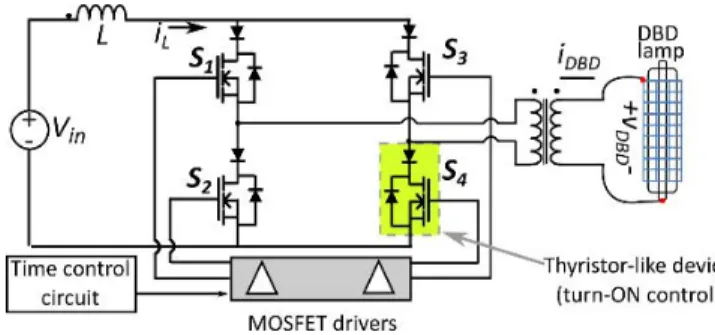
Fig. 2. Schematic of the bipolar square voltage supply.
nature, the use of a voltage-mode supply makes the control of the iDBDcurrent highly dependent on the DBD characteristics and on the performances of the power supply semiconductors (e.g., the S1. . . S4 bridge switches in Fig. 2), thus making difficult to accurately manage the lamp power and perfor-mance [12].
Therefore, during the last years several research works con-cerning the DBD lamps have been focused on current-mode supplies of different topologies, including hard switching and resonant approaches [14]–[16].
In this paper, with the aim to propose experimental evidence of the impact of the supply strategy over the DBD lamp oper-ation and over the lamp-supply performance, a Xe–Cl DBD exciplex UV lamp, filled at approximately 160 mbar of pressure, is supplied under similar operating conditions using voltage-mode and current-mode excitation methods.
In this paper, first the excitation methods are explained, discussing the pros and cons. Next, the lamp and system performance measurements are described, and finally, the lamp performance in terms of UV production efficiency and the system efficiency, obtained for each type of electrical generator, is presented.
II. DBD LAMPEXCITATIONMETHODS
For this comparative study the DBD exciplex UV lamp is operated at frequencies of 60, 80, and 90 kHz and in the 40–130 W power range. These operating points are selected on the basis of previous researches concerning the DBD lamps operation and the impact of the operating point over their performance [17]. After characterization of the employed DBD lamp an equivalent electrical model with Cd = 80 pF,
Cg= 30 pF, and Vth= 1350 V was obtained [15].
Different DBD lamp operating points are achieved by means of three different topologies: 1) a short bipolar voltage pulses supply (SBVP); 2) a pulsed current, semiresonant inverter (SRI); and 3) a pulsed current, boost-based resonant converter. From the point of view of the load, the output current magnitude and waveform are the main differences between different approaches.
All the employed supply topologies operate from a dc volt-age source; each one of them has been already described in [15]; consequently, only a brief description is presented here.
A. Short Bipolar Voltage Pulses
Power supplies of the sinusoidal and pulsed voltage type provide a simple and low-cost approach to drive DBDs.
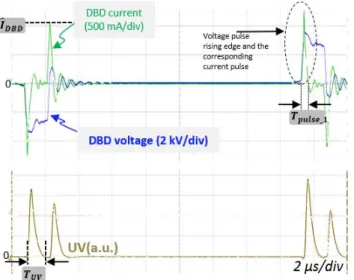
Fig. 3. DBD current, voltage, and UV waveforms obtained for a particular operating point with the short bipolar pulse excitation method. f = 60 kHz,
PDBD= 74 W, and lamp efficiency = 6.4%.
In particular, due to the capacitive nature of the DBD, the rising and falling edges of high slew-rate pulses generate very short-high intensity current spikes, which are found to promote the plasma homogeneity [18], [19].
For the SBVP generator designed for this paper, the voltage pulses are generated using a dc voltage source (240–390 V) connected to a classical four switches (MOSFETs with antipar-allel diodes) full-bridge inverter. In order to adapt the DBD voltage required level (kV) to the capabilities of the commer-cially available semiconductors, a stepup transformer (Fig. 2) is introduced in the power chain.
This transformer must be optimized so as to minimize its parallel strain capacitance Cp: this value should be, ideally,
negligible when compared to the DBD equivalent capacitor Cd and Cg, in order to reduce the impact of the transformer
parasitic elements over the efficiency. Similarly, its magne-tizing inductance Lm, should have a high impedance value,
in order to reduce the part of the transformer primary winding current which is diverted in this parallel branch.
Details concerning the special design of a transformer with these characteristics can be found in [20]. The transformer constructed for this implementation has a 1:10 turns ratio, according to the voltage level to be applied on the transformer primary side, and uses an ETD59/N87-ferrite core.
The time control circuit (Fig. 2) generates the switching sig-nals for the drivers of the two half-bridges (S1–S2and S3–S4), in order to obtain a differential output voltage across the pri-mary winding of the transformer, made of short+Vinor−Vin pulses separated by long 0-V levels, as shown on the exper-imental waveforms of Fig. 3. The drivers incorporate an internal dead-time generator avoiding any short-circuit current within each switching cell. In such a way, high-voltage pulses with 2μs of duration and alternate polarity are formed on the secondary winding of stepup transformer.
1) Duration of the Voltage Pulses: DBD lamp is an electri-cal load of capacitive character; thus according to the capacitor current expression, current flows through the DBD only during
the rising or falling fronts of voltage (differentiating circuit); the current magnitude depends on the voltage pulse rise and fall slopes and on the capacitance of the DBD reactor.
The slew rate of the voltage pulses depends mainly on the switching times (turn ON or turn OFF) of the semiconductor switches and on the transformer characteristics—the charac-teristics of the driving circuits have to be carefully selected in order to control the semiconductors switching. Additionally, as observed in the topology presented in Fig. 2, the voltage pulse is applied to the primary side of the stepup transformer; therefore, the leakage inductance is seen in series, limiting the current slope imposed to the lamp. Particularly for this implementation, the supply is tuned to obtain a lamp current pulse duration around 700 ns; however, this time is not easy to be controlled and is affected by the operating point.
Current pulses in the DBD device only take place during the fronts of thevDBD voltage; consequently, using long duration voltage pulses for DBD lamp excitation is void of reason. Furthermore, decreasing the excitation voltage pulses duration allows decreasing the number of transformer turns of both windings and decreasing of core size; hence, it leads to an efficiency gain in terms of losses in the transformer.
2) Necessity of Pauses Between Current Pulses: A sine-voltage power supply or other long pulse one has long current pulses that lead to the discharge contraction. This is known to cause a reduction in the lamp efficiency [21]. The gas discharge contraction can be limited by the use of short duration current pulses followed by long pauses allowing plasma relaxation.
3) Mitigating Considerations: In this voltage inverter topology, the semiconductors are encountering hard switch-ing mode. This mode is characterized by significant losses into transistors and additionally produces high-frequency harmonics in the transformer, which are associated with an increment in the winding losses due to the eddy-current phenomenon [22], [23].
In the other side, from the DBD point of view, the lamp current presents damped oscillations which are not able to effectively sustain the discharge and the UV production, thus contributing only to increase conduction losses.
4) UV Generation: As can be observed on the experimental waveforms of Fig. 3, UV emission takes place only when a current is flowing through the DBD bulb. The UV waveform shows a very tight correlation between the magnitudes of the current (absolute value) and of the UV pulses [11].
B. Pulsed Current SRI
In this topology the dc voltage source is connected, by means of the S1–S4 switches of a current inverter bridge, in series with the DBD and an inductance L to produce a resonant circuit. As in the pulsed voltage supply, the voltage rating of the selected semiconductors makes indispensable the use of a specially designed stepup transformer between the bridge and the DBD. The transformer constructed for this implementation has a 1:10 turns ratio and an E80-38-20/3F3 ferrite core. The transformer is designed to withstand the
ˆVDBDvoltage, which depends on the magnitude of the supplied current.
Fig. 4. Schematic of the circuit implementing the pulsed current SRI.
Fig. 5. Pulsed current SRI semicycle equivalent circuits. (a) Before gas breakdown. (b) After gas breakdown. (c) Switches spontaneously turnOFF.
Fig. 6. Waveforms obtained for a particular operating point with the pulsed current SRI. f = 80 kHz, PDBD= 56 W, and lamp efficiency = 4.7%.
The converter implementation shown in Fig. 4 operates as follows: the inductance current iL has an initial null
value. Then, turning ON the switch pair S1, S4, the resonant circuit formed by the inductance L and the lamp equivalent capacitance is connected [Fig. 5(a)]. In consequence, iL rises
following an almost semisinusoidal shape (shown in Fig. 6) and producing the gas breakdown [Fig. 5(b)]. Once the current returns to zero, the switches S1, S4 spontaneously turn OFF bringing to an end the resonance [Fig. 5(c)]. The next half cycle begins when the switches pair S2, S3 is turned ON, and produces a negative current pulse in the DBD. The zero-current switching is achieved thanks to the use of thyristor-like switches (S1–S4), implemented here with DIODE-MOSFET series connections [24].
Note that, even if the shape of the DBD lamp voltage is similar to a sinus, the DBD is not being driven by a voltage supply but by a current source of the resonant type. Accordingly, the DBD voltage is a consequence of the current waveform which imposes long-duration current pulses.
Fig. 7. Schematic of the circuit implementing the pulsed current, boost-based resonant converter.
Fig. 8. Boost-based resonant, semicycle equivalent circuits. (a) Before gas breakdown. (b) After gas breakdown. (c) Switches spontaneously turnOFF.
Fig. 9. Waveforms obtained for a particular operating point with the Boost-based resonant supply. f = 80 kHz, PDBD = 68 W, and lamp
efficiency= 5.2%.
UV Generation: The iDBD current and UV emission pulses are much longer with this supply mode than with the bipolar square voltage source 1), and a precise observation of both waveforms is much easier. It happens that the correlation between the DBD current and the UV power, observed on Fig. 3 needs to be nuanced: indeed, the UV pulses only start once the gas breakdown has occurred. In fact the UV emission is controlled by the gas current (iG current, as defined on
the equivalent circuit of Fig.1 scheme). This mechanism has already been highlighted in [11].
C. Pulsed Current Boost-Based Resonant Converter
This boost-based converter is implemented with the circuit diagram of Fig. 7. Differing from the SRI scheme, in this converter the switching sequence incorporates an additional phase of energy storage in the inductance, as follows.
Turning ON the switches pair S1, S2, [Fig. 8(a)] the inductance current rises linearly [Fig. 9 (red plot)] during
a controlled time Tch. This allows to control the amount of energy stored in L (iL2L/2); when the switch S3is turnedON, which causes simultaneously the spontaneous S2 turn OFF, a resonant circuit is formed producing the energy transfer to the DBD [Fig. 8(b) and (c)].
Note that differing from the SRI converter presented in 2), the initial value of the lamp current is not zero, thus there is hard switching at the switch S3turn ON. The experimental waveforms obtained for this converter are shown in Fig. 9.
UV Generation: Similar observations as for the SRI supply, concerning the control of the UV emission by means of the iG gas current can be done on the waveforms of Fig. 9.
III. CONTROLLABILITY OF THEUV EMISSION The experimental waveforms presented in Section II (Figs. 3, 6, and 9) have underlined the prominent role of the current injected into the DBD bulb with respect to the UV emission. Actually, only the iGconduction current which flows
through the gas takes part into the electrical power transfer toward this medium. Current leakage, which is subtracted from the current delivered by the power supply, takes place mainly in the parasitic capacitance of the high-voltage winding of the transformer [20]. Additionally, one should remember that the whole iDBD current does not flow through the gas: when the discharge isOFF, this current flow through the Cgascapacitance (displacement current).
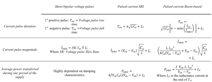
Keeping in mind these implications related to the DBD nature, a capability of the power supply to control the iDBD current and the power delivered to the DBD during each pulse is a really desirable feature. The formulas presented in Table I are summarizing the properties of each topology.
A set of remarks and comparisons can be done.
It appears that the first topology (voltage supply) does not offer a very flexible way to adjust the magnitude and the duration of the current pulses which take place at each front of the square voltage, as these values depend on noncontrolled parameters like the switching characteristics of the selected semiconductors. However, thanks to the stiff fronts of the voltage pulses, this topology allows to obtain high values of lamp peak current and consequently high instantaneous UV power.
In the case of the SRI and boost-based resonant topologies, the magnitude and the duration of the current pulses can be adjusted by means of the inductance value L or with the input voltage Vin. As seen in the power formulas, for both topologies, stability is assured only if Vin is smaller than the Vth voltage (seen in the primary), thus limiting the amount of power that can be supplied and the UV power to be obtained [25], [26].
IV. MEASUREMENTCONDITIONS
The measurement of the UV average power density is obtained with the GIGAHERTZ-OPTIK P-9710 radiometer (UV-3711-308 sensor head), placed at 3 mm of the lamp surface, on the bottom side and configured with an integration time of 0.5 s and a dose time of 5 s. Accordingly, the lamp UV power (PUV) is calculated multiplying the UV power density
TABLE I TOPOLOGIESFORMULAS
Fig. 10. Experimental bench.
measurement,ρUV (obtained with the radiometer), by the area of the virtual cylinder of radius rvc [Fig. 10 (bottom)] which surface is tangent to the radiometer detector and which length Llpis equal to the one of the lamp external electrode (metallic mesh).
In the other side, the UV emission waveforms are recorded through a PDA-25K Thorlabs photodetector (maximal sen-sitivity in the 105–550-nm range, well fit for the Xe–Cl gas mixture, which produces an UV emission at 308 nm). Fig. 10 presents the experimental arrangement.
The DBD current and voltage electrical signals are acquired using high speed current probes (Lecroy AP015) and a high-voltage differential probe (TESTEC TT-Si9010A), respectively; the phase shifts between the actual quantities and their measurement introduced by the voltage and current probes are compensated in the oscilloscope. Both signals are multiplied and the result is averaged to obtain the lamp electrical power measurement (averaging time 1 ms).
V. PERFORMANCEANALYSIS
The impact of different supply methods is analyzed by measurement and comparison of the exciplex lamp efficiency and the supply electrical efficiency, under similar operating conditions of operating frequency and DBD power.
As reported in [17], the lamp temperature has a strong impact over the UV radiation; hence for this paper, the external electrode temperature is kept around 40 °C. For a sealed-off DBD bulb, expected lifetime is around 8000 h [27]; therefore, the lamp aging during these experiments is neglected. A. Excilamp Efficiency
The exciplex lamp efficiency ηlp is calculated as the UV output power PUV, divided by the lamp electrical power PDBD
ηlp= PUV PDBD = ρUV· A PDBD . (1) The experiments are performed for operating points pro-viding a uniform discharge distribution over the electrodes area [Fig. 10(bottom)].
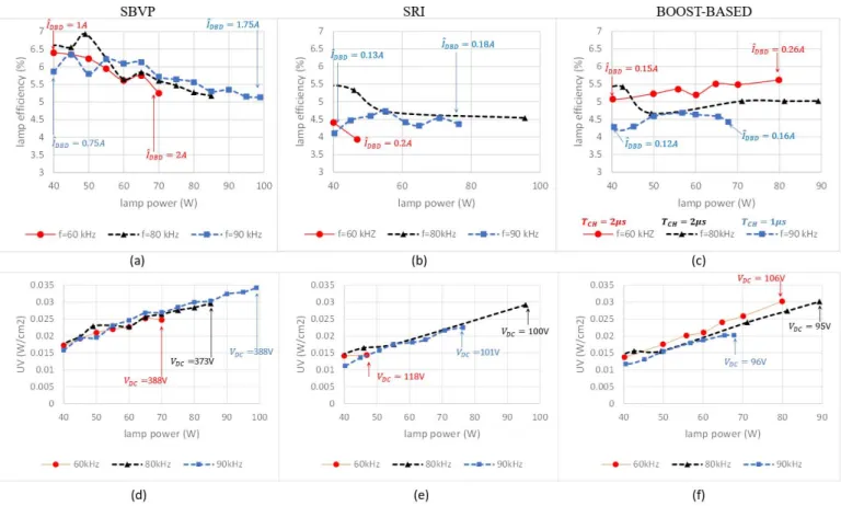
For the SBVP [Fig. 11(a)], the exciplex lamp efficiency presents a decrease with the electrical power following a linear trend as shown in Fig. 11, reaching a maximum efficiency of 7% and a minimum of 5% for 130 W of electrical power transferred to the DBD (PDBD). An important impact of the operating frequency is not appreciated.
In contrast, for the boost type supply the lamp efficiency slightly increase with PDBD. This can be attributed to the
Fig. 11. DBD UV lamp efficiency and UV power density for different excitation methods under study. (a) and (d) Pulsed voltage. (b) and (e) Pulsed current SRI. (c) and (f) Pulsed current Boost based.
Fig. 12. Power supply efficiency for different excitation methods under study. (a) Pulsed voltage. (b) and (c) Pulsed current.
fact that for the levels of current obtained for this topology a significant increment of the lamp efficiency happens as
ˆIDBD rises; from previous experiments employing a square-shaped current supply, an important augmentation of the lamp efficiency has been achieved by employing more intense current pulses [15].
For all the excitation methods, a slight decrease in the lamp efficiency with the operating frequency increment is observed. From these results is found that the square voltage supply has allowed to obtain an UV output power up to 30% higher when compared with the other excitation methods at similar values of lamp electrical power, i.e., PDBD= 70 W at 90 kHz [comparing Fig. 11(d)–(f)].
Also, among the three methods the highest lamp power has been delivered with the SBVP. This fact is explained by the stability constraints imposed by the resonant schemes (Vin< Vth/n). This constraint, limiting the maximum dc input voltage that can be applied, also limits the power to be obtained with these supplies (for a given operating frequency). In contrast, with SBVP approach there are no similar con-straints for stability.
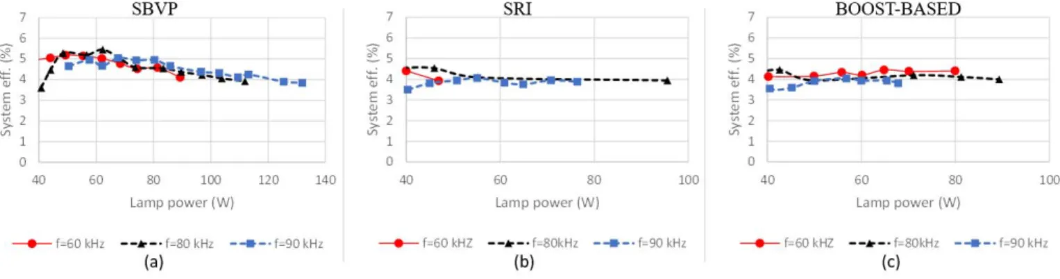
B. Supply Efficiency
The supply efficiency is computed as the ratio between the lamp electrical power and the power delivered by the dc voltage source. For different supply topologies, the impact
Fig. 13. Exciplex DBD lamp-power supply system efficiency for different excitation methods under study. (a) Pulsed voltage. (b) and (c) Pulsed current.
of the operating frequency over the supply efficiency is not noticeable as observed in Fig. 12. For the SBVP and the boost-based converters, the efficiency slightly decreases with the output power, nevertheless for the SRI converter, the efficiency has shown a marginal increment. Overall, the most efficient supply from the electrical point of view is the SRI converter. However, when comparing the system efficiency (Fig. 13), result of multiplying the supply and the lamp efficiency, it is found that the short bipolar pulses excitation method provides the highest one. For Plp= 80 W, the SBVP provides approximately 5% of efficiency against 4% with the other methods, meaning an increment of up to 20% in the UV output for this operating point. In the other side, to reach the same level of UV power, the SBVP supply requires an input voltage almost four times higher than to operate the SRI and the boost converters, with 373, 100, and 95 V, respectively, [Fig. 11(d)–(f), for UV= 30 mW/cm2at 80 kHz].
VI. FINALDISCUSSION
At comparing the efficiency of the exciplex lamp excited by three sources with different strategies, the following result is obtained: the highest energy conversion efficiency of excitation energy to the UV light was obtained by using an SBVP power supply where short current and pauses between pulses limit the contraction of the gas discharge; however, despite its simplicity, a voltage source does not allow to accurately predict and control the power injected into a DBD; thus this solution should be used in a scenario where a fine tuning of the couplings between the supply and the DBD is possible.
On the other side, the efficiency of the power supplies with resonant topology is higher than that the SBVP one, they require lower input voltage and provide more control para-meters to adjust the lamp power. In contrast, the efficiency of the complete systems (power supply + lamp) is approximately the same (4.5%).
Finally, it is interesting to point out that this paper, devoted to exciplex molecules radiation, complements previous inves-tigations reporting significant enhancement of the lamp perfor-mance with pulsed mode supplies, for lamps where radiation is mainly obtained from excimer molecules (both for DBD [28] and non-DBD reactors [29]); as formation of excimer and exciplex molecules are based on different mechanisms and
evidence of an impact of the supply method over the exciplex molecules formations was found in this research, further studies about this impact are recommended.
REFERENCES
[1] W. Siemens, “Ueber die elektrostatische Induction und die Verzögerung des Stroms in Flaschendrähten,” Ann. Phys., vol. 178, no. 9, pp. 66–122, 1857.
[2] G. Vezzu, J. L. Lopez, A. Freilich, and K. H. Becker, “Optimization of large-scale ozone generators,” IEEE Trans. Plasma Sci., vol. 37, no. 6, pp. 890–896, Jun. 2009.
[3] A. Voronov, “Mercury free UV-light sources based on excimer lamps,” in Proc. 17th Int. Conf. Gas Discharges Appl. (GD), 2008, pp. 501–504. [4] M. Vandamme et al., “Antitumor effect of plasma treatment on U87 glioma xenografts: Preliminary results,” Plasma Process. Polym., vol. 7, nos. 3–4, pp. 264–273, Mar. 2010.
[5] G. Fridman et al., “Blood coagulation and living tissue sterilization by floating-electrode dielectric barrier discharge in air,” Plasma Chem.
Plasma Process., vol. 26, no. 4, pp. 425–442, Aug. 2006.
[6] K. Heuer et al., “The topical use of non-thermal dielectric barrier discharge (DBD): Nitric oxide related effects on human skin,” Nitric
Oxide, vol. 44, pp. 52–60, Jan. 2015.
[7] T. Kuroki, T. Oishi, T. Yamamoto, and M. Okubo, “Bromomethane decomposition using a pulsed dielectric barrier discharge,” IEEE Trans.
Ind. Appl., vol. 49, no. 1, pp. 293–297, Jan./Feb. 2013.
[8] G. Matafonova and V. Batoev, “Recent progress on application of UV excilamps for degradation of organic pollutants and microbial inactivation,” Chemosphere, vol. 89, no. 6, pp. 637–647, Oct. 2012. [9] A. Oda, Y. Sakai, H. Akashi, and H. Sugawara, “One-dimensional
modelling of low-frequency and high-pressure Xe barrier discharges for the design of excimer lamps,” J. Phys. D, Appl. Phys., vol. 32, no. 21, p. 2726, Nov. 1999.
[10] C. B. Viejo et al., “Comparison between different discharge lamp models based on lamp dynamic conductance,” IEEE Trans. Ind. Appl., vol. 47, no. 4, pp. 1983–1991, Jul. 2011.
[11] H. Piquet, S. Bhosle, R. Diez, and M. V. Erofeev, “Pulsed current-mode supply of dielectric barrier discharge excilamps for the control of the radiated ultraviolet power,” IEEE Trans. Plasma Sci., vol. 38, no. 10, pp. 2531–2538, Oct. 2010.
[12] R. Díez, J.-P. Salanne, H. Piquet, S. Bhosle, and G. Zissis, “Predictive model of a DBD lamp for power supply design and method for the automatic identification of its parameters,” Eur. Phys. J. Appl. Phys., vol. 37, no. 3, pp. 307–313, 2007.
[13] C. Monge-Dauge, F. Clement, P. Svarnas, J. Loiseau, A. Ricard, and B. Held, “Experimental study coupled with electrical modeling for the consideration of DBD-based plasma jet,” IEEE Trans. Plasma Sci., vol. 40, no. 9, pp. 2254–2260, Sep. 2012.
[14] X. Bonnin, H. Piquet, N. Naudé, M. C. Bouzidi, N. Gherardi, and J.-M. Blaquière, “Design of a current converter to maximize the power into homogeneous dielectric barrier discharge (DBD) devices,” Eur.
Phys. J. Appl. Phys., vol. 64, p. 10901, Jul. 2013.
[15] R. Diez, H. Piquet, D. Florez, and X. Bonnin, “Current-mode approach in power supplies for DBD excilamps: Review of 4 topologies,” IEEE
[16] M. Meisser, R. Kling, and W. Heering, “Universal resonant topology for high frequency pulsed operation of dielectric barrier discharge light sources,” in Proc. 26th Annu. IEEE Appl. Power Electron. Conf.
Expo. (APEC), Mar. 2011, pp. 1180–1187.
[17] D. Florez, R. Diez, and H. Piquet, “Optimizing the operation of DBD excilamps,” IEEE Trans. Plasma Sci., vol. 44, no. 7, pp. 1160–1168, Jul. 2016.
[18] V. Tarasenko et al., “UV and VUV excilamps with high peak power,”
J. Light Vis. Environ., vol. 35, no. 3, pp. 227–233, 2011.
[19] A. S. Taleghani, A. Shadaram, and M. Mirzaei, “Effects of duty cycles of the plasma actuators on improvement of pressure distribution above a NLF0414 airfoil,” IEEE Trans. Plasma Sci., vol. 40, no. 5, pp. 1434–1440, May 2012.
[20] X. Bonnin, H. Piquet, R. Diez, and D. Florez, “Designing the high voltage transformer of power supplies for DBD: Windings arrangment to reduce the parasitic capacitive effects,” in Proc. 15th Eur. Conf. Power
Electron. Appl. (EPE), 2013, pp. 1–9.
[21] M. Makarov and Y. Bychkov, “The dynamics of XeCl discharge con-traction,” J. Phys. D, Appl. Phys., vol. 29, no. 2, p. 350, 1996. [22] D. Murthy-Bellur and M. K. Kazimierczuk, “Winding losses caused
by harmonics in high-frequency flyback transformers for pulse-width modulated dc-dc converters in discontinuous conduction mode,” IET
Power Electron., vol. 3, no. 5, pp. 804–817, Sep. 2010.
[23] J. Smajic, J. Hughes, T. Steinmetz, D. Pusch, W. Mönig, and M. Carlen, “Numerical computation of Ohmic and eddy-current winding losses of converter transformers including higher harmonics of load current,”
IEEE Trans. Magn., vol. 48, no. 2, pp. 827–830, Feb. 2012.
[24] M. Cousineau, R. Diez, H. Piquet, and O. Durrieu, “Synthesized high-frequency thyristor for dielectric barrier discharge excimer lamps,” IEEE
Trans. Ind. Electron., vol. 59, no. 4, pp. 1920–1928, Apr. 2012.
[25] D. Florez, R. Diez, and H. Piquet, “DCM-operated series-resonant inverter for the supply of DBD excimer lamps,” IEEE Trans. Ind. Appl., vol. 50, no. 1, pp. 86–93, Jan./Feb. 2014.
[26] R. Diez, H. Piquet, S. Bhosle, J.-M. Blaquière, and N. Roux, “Design of a current converter for the study of the UV emission in DBD excilamps,” in Proc. IEEE Int. Symp. Ind. Electron. (ISIE), Jun./Jul. 2008, pp. 62–67. [27] E. A. Sosnin, S. M. Avdeev, V. F. Tarasenko, V. S. Skakun, and D. V. Schitz, “KrCl barrier-discharge excilamps: Energy characteristics and applications (Review),” Instrum. Experim. Techn., vol. 58, no. 3, pp. 309–318, May 2015.
[28] R. J. Carman, R. P. Mildren, B. K. Ward, and D. M. Kane, “High-pressure (>1 bar) dielectric barrier discharge lamps generating short pulses of high-peak power vacuum ultraviolet radiation,” J. Phys. D,
Appl. Phys., vol. 37, no. 17, pp. 2399–2407, Sep. 2004.
[29] E. Robert, S. Point, S. Dozias, R. Viladrosa, and J. M. Pouvesle, “Study of pulsed neon–xenon VUV radiating low pressure plasmas for mercury free fluorescent sign optimization,” J. Phys. D, Appl. Phys., vol. 43, no. 13, p. 135202, 2010.
David Florez (M’12) received the B.S. degree in
electronics engineering from Pontificia Universidad Javeriana, Bogotá, Colombia, the M.S. degree in critical systems and networks from Université Paul Sabatier, Toulouse, France, and the Ph.D. degrees in electrical engineering from the Pontificia Universidad Javeriana and from the Institut National Polytechnique de Toulouse, Toulouse, France, in 2014.
He is currently a Professor and a Researcher with the Escuela de Ciencias Exactas e Ingeniería, Universidad Sergio Arboleda, Bogotá.
Dmitry Schitz received the bachelors’ degree in
radio-physics from the Tomsk State University, Tomsk, Russia, in 1998, and the Ph.D. degree in optics from the Institute of High Current Electronics, Siberian Branch of the Russian Academy of Sci-ences (SB RAS), Tomsk, in 2003.
From 1998 to 2013, he was with the Insti-tute of High Current Electronics, SB RAS. He is currently the Head of the Laboratory of Optical Radiation, Immanuel Kant Baltic Federal University, Kaliningrad, Russia. His current research interests include medicine equipment based on radiation of cold gas-discharge plasma.
Hubert Piquet was born in Arras, France, in 1960.
He received the B.S. degree in applied physics from Ecole Normale Supérieure de Cachan, Cachan, France, in 1984, and the Ph.D. degree in electrical engineering from the Institut National Polytechnique de Toulouse, Toulouse, France, in 1990.
He is currently a Full Professor with the Insti-tut National Polytechnique de Toulouse, where he teaches courses on power electronics and systemic approach in electrical engineering. He is involved in research at the Laboratoire Plasma et Conversion d’Energie, Toulouse. His current research interests include electrical embed-ded networks as well as power supplies for plasma applications.
Rafael Diez (SM’15) received the B.S. degree in
electronics engineering from Pontificia Universidad Javeriana, Bogotá, Colombia, in 2001, and the M.S. and Ph.D. degrees from the Université de Toulouse, Toulouse, France, in 2005 and 2008, respectively.
He is currently an Assistant Professor with the Department of Electronics Engineering, Pontificia Universidad Javeriana. His current research interests include the development of power converters for electric discharges.