HAL Id: hal-02417678
https://hal.archives-ouvertes.fr/hal-02417678
Submitted on 18 Dec 2019
HAL is a multi-disciplinary open access
archive for the deposit and dissemination of
sci-entific research documents, whether they are
pub-lished or not. The documents may come from
teaching and research institutions in France or
abroad, or from public or private research centers.
L’archive ouverte pluridisciplinaire HAL, est
destinée au dépôt et à la diffusion de documents
scientifiques de niveau recherche, publiés ou non,
émanant des établissements d’enseignement et de
recherche français ou étrangers, des laboratoires
publics ou privés.
System for experimental investigation of DBD excilamps
in view of control and optimization of UV emission
Arnold Wiesner, Rafael Diez, David Florez, Hubert Piquet
To cite this version:
Arnold Wiesner, Rafael Diez, David Florez, Hubert Piquet. System for experimental investigation of
DBD excilamps in view of control and optimization of UV emission. Mathematics and Computers in
Simulation, Elsevier, 2019, 165, pp.92-106. �10.1016/j.matcom.2019.02.021�. �hal-02417678�
OATAO is an open access repository that collects the work of Toulouse
researchers and makes it freely available over the web where possible
Any correspondence concerning this service should be sent
to the repository administrator:
tech-oatao@listes-diff.inp-toulouse.fr
This is an author’s version published in:
http://oatao.univ-toulouse.fr/24164
To cite this version:
Wiesner, Arnold and Diez, R. and Florez, David and Piquet,
Hubert System for experimental investigation of DBD
excilamps in view of control and optimization of UV emission.
(2019) Mathematics and Computers in Simulation, 165.
92-106. ISSN 0378-4754
Official URL:
https://doi.org/10.1016/j.matcom.2019.02.021
System
for experimental investigation of DBD excilamps in view of
control
and optimization of UV emission
A. Wiesner
a,b,∗,
R. Diez
a,
D. Florez
a,c,
H. Piquet
ba Pontificia Universidad Javeriana, Carrera 7 No. 40-62, 110231 Bogotá, Colombia
b LAPLACE, Université de Toulouse, CNRS, INPT, UPS, 2 rue Charles Camichel, 31071 Toulouse, France cUniversidad Sergio Arboleda, Calle 74 No. 14-14, 110221 Bogotá, Colombia
Abstract
This paper presents the design of a system aimed at characterizing a diverse set of dielectric barrier discharge UV lamps. This experimental bench allows the study of the lamps performances regarding UV emission maximization and energy conversion optimization. It includes a current-mode pulsed power supply for the lamps, the design of which is detailed. This converter presents 3 degrees of freedom (DOF) can control and adjust independently the frequency, amplitude and duration of the current pulses injected into the lamps. Theoretical modeling of the lamps, by means of equivalent electrical circuits, is used to define the most interesting operating points to be explored, as well as for the converter’s design; these models are afterwards validated by experimental tests on the entire set of lamps. The operation of the bench is controlled by a supervising program: the latter manages the data acquisition and performs sweeps of the DOFs of the pulsed current. Examples of analyzes, oriented toward optimization of electric to UV energy conversion, are shown.
Keywords: DBD; Power converters; Current-mode; Interleaved converters
1. Introduction
Dielectric Barrier Discharge (DBD) UV lamps are environmentally friendly (mercury free) UV sources with various applications, as disinfection, microelectronics, surface treatment, and skin phototherapy. The practical usefulness and applicability of currently available DBD excilamps has been demonstrated [16,21]; today, studies oriented toward their performance improvement are in development. This can be achieved by means of the reactor design optimization (geometry, filling mixture, pressure and materials) [3,6,11,17,24], and also by choosing the proper electrical operating conditions [4,8,13,14,18,19,25]. The approach developed in this paper is aimed at performing system level optimization, integrating in the same step DBD reactor and power supply designs.
The impact of the electrical operating point (OP) over the DBD excilamps performance has been already reported by different teams [1,10,20,21]. However, because the geometrical and gas mixture parameters of a DBD excilamp
∗ Corresponding author at: Pontificia Universidad Javeriana, Carrera 7 No. 40-62, 110231 Bogot´a, Colombia. E-mail addresses: awiesner@javeriana.edu.co(A. Wiesner), rdiez@javeriana.edu.co(R. Diez).
Fig. 1. DBD lamp geometry.
Fig. 2. DBD characterization system.
cannot be easily adjusted [9] and constructed, most of these studies are developed for a fixed lamp design. The impact of the DBD lamp geometry over the system’s performances has not been widely reported.
Considering that maximization and optimization of the UV production is one objective of research groups working with excimer lamps, the development of a system able to vary the electrical parameters in the discharge, and having the possibility to characterize different DBD lamps is proposed here. This test bench needs to be versatile, in order to supply different DBDs under various operative conditions; it also varies the supply’s characteristic and collects the measurements, in view of performances analysis and improvement. In this document the test-bench design is detailed and a prototype, tested for a set of UV excimer lamps, is presented.
With the aim to provide deeper insight and experimental evidence about the UV production dependence on the geometry of the DBD reactor, a set of nineteen diverse DBD exciplex UV lamps of coaxial type, has been built. As shown inFig. 1, the bulbs differ with the values of, T, the dielectric walls thickness, a the internal radius, b the external radius and l the length. Each one of the 19 bulbs presents a different set of geometrical parameters {T, a, b, l}; they all are filled with the same Xe-Cl gas mixture, under the same pressure.
The proposed study includes the design of a static converter capable of supplying these 19 different excilamps at different controlled electrical operating points. Additionally, the test-bench must be able to measure for each experiment the required variables in order to compare the performance of the lamps, in terms of the obtained UV power and also of the electrical to UV power conversion efficiency. The block diagram of the proposed system is displayed inFig. 2and can be divided in two main parts: the power supply and the acquisition interface.
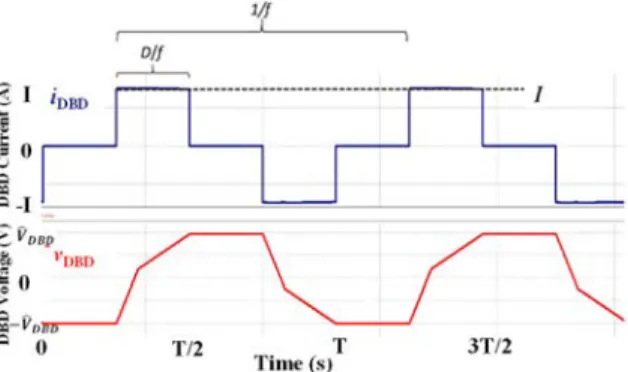
From previous works a significant impact of the supplying conditions over the lamps performance has been evidenced. Particularly, the methodology proposed in [8,13] makes use of a square-shape current waveform for the
parametric study of DBDs. By means of the lamp current waveform (iD B D), the lamp power can be controlled
with three degrees of freedom (DOFs): duty cycle (D), current intensity (I) and frequency (f ) of the current pulses,
as shown in Fig. 3. Accordingly, the power electronic modules must be capable to deliver and vary these three
Fig. 3. DBD current and voltage waveforms using a square-shape current source.
The power supply consists of a DC adjustable current source in cascade with a full-bridge current inverter [8]. A step-up transformer is used to connect the bulb to the current inverter, in order to adapt the DBD peak voltage to the rating of the semiconductors.
The dimensioning and implementation of power supply converters for the proposed study is a challenge due to the wide range of the operating conditions imposed by the set of 19 lamps. According to the dimensions of the bulbs, the power range of this supply has been chosen to be from 0 to 500 W.
The power supply design process is presented in the following sections: first, the electrical model of each lamp is theoretically obtained as a basis for the converter design. Then, using this model and taking into account the different characteristics of the 19 bulbs, the operating range of interest, concerning the properties of the current pulses, is determined. Finally, the converter design is presented, pointing out the challenges of supplying such a different set of loads at this level of power (up to 500 W).
The second part of the test-bench, the acquisition interface, is a software that stores the measurements of the DBD instrumentation. It also sends the OP request (f, D and I) to the converters via the control board (FPGA), as shown inFig. 2. Details about this interface are given in Section4.
2. DBD lamps under study
The nineteen coaxial DBD lamps, used for this work, present the configuration shown inFig. 1. and have different geometrical parameters that are categorized as:
• External diameter: with two different values, 25 mm and 45 mm.
• Internal diameter: six different values varying from 5 mm to 30 mm in steps of 5 mm.
• Thickness of the dielectric barriers: three different values, 1 mm, 1.5 mm and 2 mm. All lamps have same
inner and outer barrier thicknesses.
All the lamps have a length (l) of 600 mm. The gas mixture used to fill the lamp bulbs is Xe-Cl, producing a radiation wavelength at 308 nm.
In order to design a power supply capable of driving all the lamps under study, initially, the electrical magnitudes are calculated using the simplified electrical model of the DBD developed in [7,22,27], as shown in Fig. 4.
In this model, Cd is the dielectric series equivalent capacitance, Cg the gas equivalent capacitance and Vt h the
gas breakdown voltage. The values of Cg and Cd are estimated using the cylindrical capacitor Eqs.(1)and(2). The
Paschen’s law in Eq.(3)is used to determine the breakdown voltage Vt h.
Cg= 2π · εg·l ln(b−T a+T ) ≈ Kg·l ln(b−T a+T ) (1) Cd = 2π · εd·l ln( a·b T2+a·T +b·T +a·b ) ≈ Kd ·l ln( a·b T2+a·T +b·T +a·b ) (2)
Fig. 4. DBD electrical model. Table 1 DBD model parameters. Range Dielectric capacitance (Cd) 94 pF–475 nF Gas capacitance (Cg) 63 pF–1 nF Threshold voltage (Vt h) 1167 V–2579 V Vt h= C · pgas·d ln ( A· pgas·d ln(1+γ1) ) ≈ Kt h·d K′+ln(d) (3)
In these equations, a, b, l and T are the geometrical parameters of the lamp, previously shown in Fig. 1; A
is a constant which depends on the electron kinetic temperature, C is related to A and to the effective ionization potential V ∗ (C = A V∗), p
gas is the gas pressure, d is the distance between dielectrics (gas gap), andγ is the
electron emission coefficient [28].
In the approximations used in these three equations, the Kg, Kd, Kt h and K′ terms are constants, which values
are derived from measurements achieved on a previously identified bulb, having the same barriers material, gas mixture and pressure [9].
With the geometry known for each lamp, the parameters of the electrical model are calculated, obtaining the ranges presented inTable 1.
3. Operating points range
Once the 19 sets of (Cd, Cg, Vt h) parameters for the electrical model are obtained, it is possible to find out the
values of the amplitude (I) of the lamp current (iD B D) and the peak voltage for each lamp, thanks to Eqs. (4)and
(5), deduced from work detailed in [3].
I = P D · Vt h + f4 · Cg·Vt h D (4) ˆ VD B D =Vt h+ I · D 4 · f · Cd (5)
Pis the desired average electric power on the DBD (which maximum has been set to 500 W); D, I, and f are
the three degrees of freedom of the iD B D current shape, controlled thanks to the current inverter (f, D) and the DC
current source ( J = I · n), n being the turns ratio of the step-up transformer.
Fig. 5presents, for the nineteen different lamps, the current pulse amplitude I, versus the f frequency for two
different duty cycles (D = 5% and D = 100%) needed, according to Eq.(4), to obtain the maximum requested
Fig. 5. Current in the 19 lamps as a function of the frequency. Cases for duty cycle of 5% (top) and 100% (bottom).
that the desired power is obtained, for D = 100%, with a relatively low I value (this value will define the operating conditions of the current inverter and the current source, considering that these converters control the J current in the primary side of the transformer). To avoid the oversizing of the current converters, the maximum value of I is set to 1.4 A. As a matter of fact, with this limitation, all the points associated with D = 5% will not reach 500 W. For this duty cycle, the specific power (power per unit of bulb length) will be maintained thanks to an outer metallic electrode of reduced length.
Combining Eqs. (4) and(5), it is possible to obtain Eq. (6), where it can be seen that the lamp peak voltage (ˆVD B D) does not explicitly depend on the duty cycle D.
ˆ VD B D =Vt h ( 1 +Cg Cd ) + P f ·4 · Cd ·Vt h (6) For the same power level P = 500 W,Fig. 6. presents the lamp peak voltage (ˆVD B D) versus frequency, for the
19 lamps.
This figure shows that the requested lamp voltage in low frequencies is up to 40 kV; thus, to avoid oversizing of the step-up transformer, the minimum operating frequency has been limited to 30 kHz. The maximum operating frequency has been set to 200 kHz, considering implementation aspects, as the speed of semiconductor devices and the limitation of magnetic materials.
Fig. 6. Lamp peak voltage as a function of the frequency.
Fig. 7. Selection of the switches via the V I product.
To conclude this section, we summarize below the operating range of the parameters for the iD B D pulses:
• 0< I < 1.4 A • 5%< D < 100% • 30 kHz< f < 200 kHz 4. Converter design
After finding the operating range for the 3 degrees of freedom (I, D, f ), that will be used to make the characterization of the DBDs, the static converter’s design is explained in this section.
4.1. Inverter switch selection
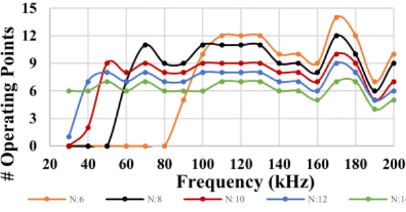
The selection of the inverter switches is performed under the assumption that the power can be delivered to the lamp independently of the transformer turns ratio, that will be chosen later. For that purpose, the product of voltage (taken fromFig. 6.) and current (taken fromFig. 5.- D = 100%) in each lamp is obtained for the most demanding case, resulting in the decaying curve shown inFig. 7. for a given lamp.
The obtained curve is compared to the product of the blocking voltage and the current rating of the candidate switches for the converter (flat lines in Fig. 7). The operating points that are above the intersection between the
Fig. 8. Operating points attained vs. the frequency for different turns ratio of the transformer.
Fig. 9. DBD system with two parallel current sources.
lamp and switch curves are the ones that cannot be attained by the switch, regardless of the transformer turns ratio.
The switch is chosen using a compromise between its price and the number of reachable OP.Fig. 6will be useful later to determine the value of the minimum operating frequency for the selected semiconductor device, keeping a blocking voltage less than the one allowed in the switch specifications.
4.2. Transformer
Once the switches have been chosen, the interesting OPs fromFig. 7are tested for different transformer turns ratios (n). The points to be discarded are the ones where the peak voltage or the current in the lamp (seen in the primary side of the transformer) exceeds the ratings of the switch. The points with power losses in the switches greater than 30 W are also removed due to thermal limitation for the available cooling system (natural convection heatsink).
Fig. 8. shows the result of this analysis and the turns ratio is selected maximizing the number of reachable points, but also assuring a wide frequency range. In this case a turn ratio of 10 is selected.
4.3. Current source
To avoid the influence of the iD B D current ripple on the DBD performance, the frequency bandwidth of the
current source which supplies the current inverter should be much higher than the maximum frequency of the latter. Since the lamp current has a maximum frequency of 200 kHz it is not possible to comply with this condition.
For this reason, parallel current choppers as shown in Fig. 9, with an interleaved configuration increases the apparent frequency of the delivered current [2,12].
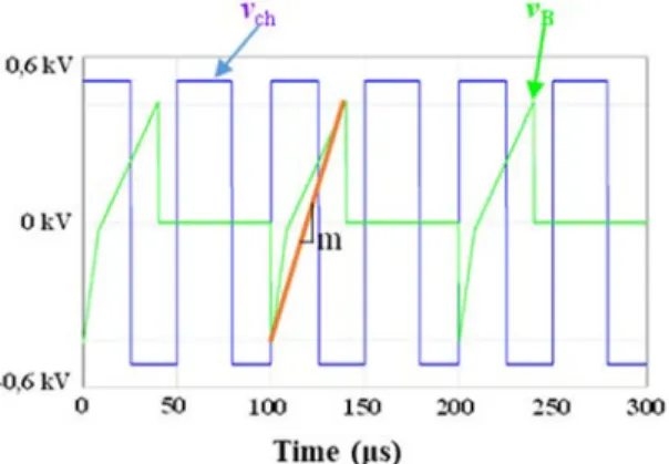
Fig. 10. Output voltage of the chopper vch and input voltage of the current inverter vB- case where fchis similar than fB. (For interpretation of the references to color in this figure legend, the reader is referred to the web version of this article.)
In addition, this parallel configuration allows to reduce the average current in each switch. The maximum DC current being J = 14 A, the average output current of both DC current sources is 7 A, seen by each of their switch. The maximum frequency of the current sources is defined by the ratings of the semiconductor devices, switching losses and the limitation of magnetic materials. The worst case in terms of current ripple happens when the maximum
frequency on the inverter and the maximum frequency on each current source are similar, as shown in Fig. 10.
This figure plots the output voltage of the chopper vch and the input voltage of the current inverter vB. L inductor
which controls the current ripple at the input of the current inverter is defined by Eqs.(7)–(10). The current ripple on the L inductor is defined by:
∆iL= 1 L ∫ t +DchTch t Vi n dt − 1 L ∫ t +DchTch t vB dt (7) ∆iL= Dch L fch ( Vi n−V0− m Dch 2 fch ) (8) Being, m ≈ 2 · ˆVD B Df n · D (9)
Assuming the approximation of the shape of the vB voltage, highlighted with the red slope (m) in Fig. 10, the
current ripple is defined by: ∆iL= Dch L · fch ( Vi n−vB−VˆD B D· f · Dch n · fch·D ) (10) vB is a voltage that varies between –ˆVD B D and + ˆVD B D as shown inFig. 10. n is the transformer’s turns ratio, f
and D are the frequency and duty cycle of the current inverter, respectively, and fch and Dch are the frequency and
duty cycle of the current sources. Note that this converter differs from conventional DC-DC converters, because vB
presents high frequency (at inverter’s frequency) bidirectional changes. This fact implies a high inductance value to maintain a low current ripple.
4.4. Current source control
The peak current mode control is chosen for the DC current sources, using the IC TPS40180. The current set point (J) is sent to this current controller from the FPGA. The current is sensed with a shunt resistor placed between the source of the low-side MOSFET and the circuit ground.
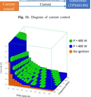
The TPS40180 controller can receive an external clock, as shown inFig. 11, allowing the synchronization of
two or more parallel current sources. The clock signals are generated by the FPGA, with a phase delay of 180◦,
Fig. 11. Diagram of current control.
Fig. 12. Possible operating points and the ones that inject between 400 W and 500 W, for one of the lamps . (For interpretation of the references to color in this figure legend, the reader is referred to the web version of this article.)
4.5. Working range
Once defined the different devices of the system, it is important to finally find out the actually accessible OP for each lamp. To do that, a cloud of OP is plotted for each lamp, varying f in steps of 5 kHz, D in steps of 5% and Iin steps of 0.2 A.
These points are discriminated with colors, as shown for a given bulb, inFig. 12: the green cells are the most interesting OP for the experiment as their power lies between 400 W and 500 W. With the blue ones the injected power is less than 400 W.
The others are eliminated for various reasons: the orange ones do not ignite the lamp; the white ones (blank spaces over the green or blue OP) are eliminated because one of the following restrictions is exceeded:
• the peak voltage across the switches is higher than the maximum allowed value;
• the power is higher than 500 W.
One should remember here that peak voltages as well as the maximum power depend on the geometrical parameters (T, a, b, l) of the bulbs; for that reason,Fig. 12shape and size change for each lamp.
4.6. Configuration and data acquisition interface
As explained in Section 1, the test-bench comprises a set of sensors, measurement instruments and also an
acquisition system (interface and storage). Electrical measurements of the excilamp voltage and current are acquired using an oscilloscope LECROY HDO4024 with voltage probes TESTEC TT-SI 9110 and current probes LECROY AP015. The lamp temperature is monitored using the Omega OS210-150-300-800 sensor. The average UV power is measured with a Gigahertz Optik P9710 optometer and the UV instantaneous response is acquired using a Thorlabs
Fig. 13. LabVIEW user interface.
PDA-25k photodetector, connected to the oscilloscope. Finally, the radiation spectrum is registered by means of an OCEAN-Optics 2000 spectrometer. All these measurements are acquired and saved for each experiment.
Once the safe operating points range for the excilamp under study is determined, the system is configured
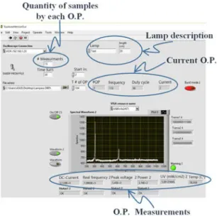
accordingly through the user interface specially developed for the test-bench, shown in Fig. 13. This interface
allows the following adjustments: the parametric sweep of the operating points (start, end and step values for each variable); the number of trials for each point and the delay between trials.
For each trial the interface saves the following measurements: the excilamp DBD average power, DBD Peak voltage, DBD frequency, DBD current intensity, DBD UV average power density, temperature and the wavelength spectrum (from 200 to 1000 nm). Also, the waveforms of voltage, current and UV are saved for each OP. Note that the system only starts the acquisition of the measurements when the system has detected that the OP introduced in the user interface is reached in the DBD excimer lamp. This means that all measurements are stable (steady state). Several measurements are taken for the same operating point, allowing data post-processing, like the computation of error and arithmetical average. Once the averages are calculated in all measurements, these values are assigned to the corresponding OP to perform the analysis of the different DBDs. It is possible to characterize the different excilamps obtaining their electrical model (Cd, Cg and Vt h), energy conversion performance and to investigate the
impact of the lamp geometry in the aspects previously mentioned. With the data saved is also possible to accomplish a statistical analysis if required.
5. Simulation and experimental test
Some experimental waveforms are presented in this section; the latter are compared with the simulation results of the lamp-supply model used for the design of the test-bench.
5.1. Comparison between theoretical, simulation and experimental results
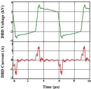
To validate the theoretical analysis of the DBD power supply, the simulation software PSIM is used. The curves
displayed inFig. 14. correspond to the OP with f = 170 kHz, D = 15%, I = 1.4 A, and the electrical model of
the DBD with the following parameters Cd =204 pF, Cg =67 pF and Vt h=2.43 kV.
For the same OP, Fig. 15. shows the experimental waveforms for the DBD voltage (VD B D) and the DBD
current (iD B D).
The simulation and the experimental tests are in good agreement with the theoretical analysis, as shown inTable 2
Fig. 14. Simulated waveforms for a specific case: VD B D(top) and iD B D (bottom).
Fig. 15. Experimental measurements for the same OP: specific case: VD B D (top) and iD B D (bottom).
Table 2
Results comparison ( f = 170 kHz, D = 15%, I = 1.4 A).
Theoretical Simulation Measures ˆ
VD B D 3.9 kV 3.4 kV 3.4 kV
P 308 W 323 W 350 W
Additionally, for the entire set of lamps a comparison is performed, between the theoretical values of the electrical model parameters (Cd,Cg and Vt h), obtained by Eqs.(1)to(3), and the experimental values, identified through the
Manley diagram [23].
Fig. 16, shows the comparison for the threshold voltage, Vt h. The lamps are labeled, in the X -axis for this figure,
from L01 to L19 and are ordered by the length of the gas gap. The lamps with big gas gaps are in good agreement
with the approximation given in Eq.(3). For small gas gap lamps, the approximation should be improved.
Fig. 17, presents results concerning the dielectric capacitance, Cd. The order in the X -axis is selected according
to the geometrical expression proposed for the approximation in Eq.(2) (ln (b−T
a+T)). This approximation has a big
error for the three first lamps, which present too small difference between the external and internal electrode (gas gap of 1 mm). As the gas gap increases the approximation is better.
Fig. 16. Comparison between experimental and theoretical values for Vt h.
Fig. 17. Comparison between experimental and theoretical values for Cd.
Fig. 18 shows the comparison for the gas capacitance. In this case the lamps are ordered according to the expression proposed in Eq.(2)(ln(T2+a·T +b·T +a·ba·b
))
, related to bulb geometry.
Figs. 16to18show that the increasing and decreasing trends are the same for the theoretical and experimental parameters of the model. However, adjustment of the approximations used for Eqs.(1)to(3)should be done, since there are considerable errors for several lamps. These errors could be a consequence of using, in the approximations, the same constants from a single identified model in previous work. The identification through the Manley’s diagram of the different lamps should improve the approximation and are a good tool for future design.
Another comparison between theoretical and experimental results is presented inFig. 19: the lamp peak voltage and the lamp power are both displayed. This figure shows the results for only one lamp and similar agreement are obtained for the other 18 lamps. These results confirm that the electric model and the values calculated theoretically are the right support for the converter design.
Fig. 18. Comparison between experimental and theoretical values for Cg.
Fig. 19. Comparison between peak voltage and power on DBD with them theoretical and experimental values.
5.2. System validation
In order to validate and put forward the capabilities of the test-bench, a parametric sweep is performed for one of the lamps and the results are shown inFig. 20. In this figure, the average UV specific power vs the electric power on the DBD is observed for different values of current intensities (I). For this experiment, 10 different measurements are taken for each operating point. Each point shown inFig. 20corresponds to the average of those 10 values. The entire set of operating points present a standard deviation of 2.3% concerning the value of the electric power and 4.9% for the UV measurement.
The results show that the same amount of electric power could deliver different values of UV radiation, implying that the three DOF (f, D and I) influence the energy conversion efficiency of the lamp, since the same electric
power could be injected to the lamp with different combinations of these three DOF as can be seen with Eq.(4).
For instance, inFig. 20, it is possible to observe the positive impact that the high values of current intensity have over the UV radiation: the green square points are mostly above the yellow diamonds and the blue circle points.
The results obtained inFig. 20are the characterization of one lamp as a function of one DOF, similar figures can be obtained for different electrical parameters. For example, inFig. 21, the current (I) is maintained at a constant level and variations of the duty cycle and the frequency (D and f ) are performed in order to point out the influence of the discharge ON-time (time during which the gas is ignited) on the UV radiation. Here, the UV radiation as a
Fig. 20. UV vs. P as a function of I for one lamp.
Fig. 21. UV as a function of the electric power with constant current amplitude.
function of the electric power is plotted again, with the discharge ON-time grouped in small ranges. Here one can observe an influence of the discharge ON-time on the energy conversion efficiency.
Results shown in last figures agree with previous experimental works, where the current amplitude and the pulse duration have an influence over the lamp efficiency [5,15,26]. This is only a sample of the possible analyses that can be performed using the test-bench developed in this paper, that will help the designers of DBD lamps and power supplies with the optimization of the system-level efficiency.
Conclusions
The procedure to design a characterization test-bench for DBD excimer lamps has been explained and validated with a set of 19 different lamps.
The theoretical modeling of the lamps, necessary to perform the dimensioning of the power supply, is found to be relatively accurate. The inverter switches are selected based on a good balance between cost and the number of interesting operating points that are attainable. The transformer turns ratio is also selected maximizing the interesting operating points that are attainable and the most desired frequency range.
According to the frequency range of the current pulses (fmax = 200 kHz), the realization of the DC current
source, which needs to present an even higher frequency is a real challenge. With the current limitations of the semiconductors, the most relevant solution is the implementation of parallel current source converters in interleaved configuration, enabling a reduction in the output current ripple and multiplying the apparent switching frequency.
The system has the capability to automatically collect data changing electrical and geometrical parameters, helping with the UV process optimization in excimer lamps.
Acknowledgments
The authors acknowledge specially to ECOS-Nord/COLCENCIAS/ICETEX French-Colombian cooperation program, ECOS Nord Program under Project C16P01, by Colciencias, Colombia under contracts 663–2015 and 294–2016 and by Universidad Sergio Arboleda, Colombia under Project IN.BG.086.16.013 and COLCEN-CIAS/COLFUTURO because part of this work is supported by them.
References
[1] H. Akashi, A. Oda, Y. Sakai, Development of streamers in dielectric-barrier-discharge excimer lamp, IEEE Trans. Plasma Sci. 36 (2008) 1336–1337.
[2] M. Bendali, C. Larouci, T. Azib, C. March, G. Coquery, Design methodology of an interleaved buck converter for onboard automotive application, multi-objective optimization under multi-physic constraints, IET Electr. Syst. Transp. 5 (2015) 53–60.
[3] C. Blanco Viejo, et al., Comparison between different discharge lamp models based on lamp dynamic conductance, IEEE Trans. Ind. Appl. 47 (2011) 1983–1991.
[4] I.V. Bozhko, Y.V. Serdyuk, Determination of energy of a pulsed dielectric barrier discharge and method for increasing its efficiency, IEEE Trans. Plasma Sci. 45 (2017) 3064–3069.
[5] R.J. Carman, R.P. Mildren, B.K. Ward, D.M. Kane, High pressure (>1 bar) dielectric barrier discharge lamps generating short pulses of high-peak power vacuum ultraviolet radiation, J. Phys. D 37 (2004) 2399–2407.
[6] K.Y. Cheng, Y.W. Yang, Z.H. Lin, G.C. Liao, C.T. Liu, J.S. Wu, A cold planar nitrogen-based atmospheric-pressure dielectric barrier discharge jet with enhanced UV emission and radical generation using short electrodes, IEEE Trans. Plasma Sci. 44 (2016) 3183–3188.
[7] R. Diez, H. Piquet, S. Bhosle, J.M. Blaquiere, Current mode converter for dielectric barrier discharge lamp, in: IEEE Power Electronics Specialists Conference, 2008, pp. 2485–2491.
[8] R. Diez, H. Piquet, D. Florez, X. Bonnin, Current-mode approach in power supplies for DBD excilamps: Review of 4 topologies, IEEE Trans. Plasma Sci. 43 (2015) 452–460.
[9] R. Díez, J.-P. Salanne, H. Piquet, S. Bhosle, G. Zissis, Predictive model of a DBD lamp for power supply design and method for the automatic identification of its parameters, Eur. Phys. J. Appl. Phys. 37 (2007) 307–313.
[10] L.T. Doanh, S. Bhosle, G. Zissis, H. Piquet, Estimation of the light output power and efficiency of a XeCl dielectric barrier discharge exciplex lamp using one-dimensional drift–diffusion model for various voltage waveforms, IEEE Trans. Ind. Appl. 49 (2013) 331–340.
[11] M.V. Erofeev, D.V. Schitz, V.S. Skakun, E.A. Sosnin, V.F. Tarasenko, Compact dielectric barrier discharge excilamps, Phys. Scr. 82 (2010) 045403.
[12] M. Esteki, B. Poorali, E. Adib, H. Farzanehfard, High step-down interleaved buck converter with low voltage stress, IET Power Electron. 8 (2015) 2352–2360.
[13] D. Florez, R. Diez, H. Piquet, Optimizing the operation of DBD excilamps, IEEE Trans. Plasma Sci. 44 (2016) 1160–1168.
[14] D. Florez, R. Diez, H. Piquet, A.K. Hay Harb, Square-shape current-mode supply for parametric control of the DBD excilamp power, IEEE Trans. Ind. Electron. 62 (2015) 1451–1460.
[15] D. Florez, D. Schitz, H. Piquet, R. Diez, Efficiency of an exciplex DBD lamp excited under different methods, IEEE Trans. Plasma Sci. 46 (2018) 140–147.
[16] E.A. García-Guerrero, et al., Use of a COAX-DBD plasma fluidized-bed reactor for surface modification of TiO2 and potato-starch powders, IEEE Trans. Plasma Sci. 46 (2018) 2425–2434.
[17] E. Gnapowski, S. Gnapowski, Changes in the power discharge in a plasma reactor using porous versus solid dielectric barriers and meshes electrodes, IEEE Trans. Plasma Sci. 44 (2016) 2079–2083.
[18] T. Guo, S. Hao, C. Zhang, J. Liu, Y. Deng, X. He, Analysis and design of pulse frequency modulation discontinuous-current-mode dielectric barrier corona discharge with constant applied electrode voltage, IET Power Electron. 7 (2014) 2857–2869.
[19] G. Huang, et al., Statistical analysis of pulsed microdischarges and ozone generation in dielectric barrier discharges, IEEE Trans. Plasma Sci. 44 (2016) 2111–2120.
[20] M.I. Lomaev, V.S. Skakun, E.A. Sosnin, V.F. Tarasenko, D.V. Shitts, M.V. Erofeev, Excilamps efficient sources of spontaneous UV and VUV radiation, Phys.-Usp. 46 (2003) 193–209.
[21] M.I. Lomaev, E.A. Sosnin, V.F. Tarasenko, Excilamps and their applications, Prog. Quantum Electron. 36 (2012) 51–97.
[22] A.M. Lopez, H. Piquet, D. Patino, R. Diez, X. Bonnin, Parameters identification and gas behavior characterization of DBD systems, IEEE Trans. Plasma Sci. 41 (2013) 2335–2342.
[23] T.C. Manley, The Electric Characteristics of Ozonator Discharge, Eighty-Fourth General Meeting held at New York, 1943, pp. 83–96.
[24] M. Meißer, Resonant Behaviour of Pulse Generators for the Efficient Drive of Optical Radiation Sources Based on Dielectric Barrier Discharges, KIT Scientific Publishing, Karlsruhe, 2013.
[25] K. Nassour, et al., Comparative experimental analysis of ozone generation between surface and volume DBD generators, IEEE Trans. Dielectr. Electr. Insul. 25 (2018) 428–434.
[26] A. Oda, Y. Sakai, H. Akashi, H. Sugawara, One-dimensional modelling of low-frequency and high-pressure Xe barrier discharges for the design of excimer lamps, J. Phys. D 32 (1999) 2726.
[27] V. Pipa, T. Hoder, J. Koskulics, M. Schmidt, R. Brandenburg, Experimental determination of dielectric barrier discharge capacitance, Sci. Instrum. 83 (2012).
[28] J. Reece Roth, Dark Electrical Discharges in Gases, Vol. 1, Industrial Plasma Engineering British Library Cataloguing, 1995, pp. 251–296.