HAL Id: hal-00491400
https://hal.archives-ouvertes.fr/hal-00491400
Submitted on 11 Jun 2010HAL is a multi-disciplinary open access archive for the deposit and dissemination of sci-entific research documents, whether they are pub-lished or not. The documents may come from teaching and research institutions in France or abroad, or from public or private research centers.
L’archive ouverte pluridisciplinaire HAL, est destinée au dépôt et à la diffusion de documents scientifiques de niveau recherche, publiés ou non, émanant des établissements d’enseignement et de recherche français ou étrangers, des laboratoires publics ou privés.
Design and Fabrication of GaInAsP-InP VCSEL with
two a-Si/a-SiNx Bragg Reflectors
Christophe Levallois, Alain Le Corre, Slimane Loualiche, Olivier Dehaese,
Hervé Folliot, Cyril Paranthoen, Christophe Labbé
To cite this version:
Christophe Levallois, Alain Le Corre, Slimane Loualiche, Olivier Dehaese, Hervé Folliot, et al.. De-sign and Fabrication of GaInAsP-InP VCSEL with two a-Si/a-SiNx Bragg Reflectors. International Workshop on PHysics & Applications of SEmiconductor LASERS, Mar 2005, Metz, France. p1. �hal-00491400�
Design and Fabrication of GaInAsP/InP VCSEL with two a-Si/a-SiN
xBragg reflectors
C. Levallois, A. Le Corre, S. Loualiche, O. Dehaese, H. Folliot, C. Paranthoen, and C. Labbé.
LENS - CNRS UMR FOTON 6082
INSA de Rennes, 20 Avenue des Buttes de Coësmes, 34043 Rennes Cedex, France e-mail: christophe.levallois@ens.insa-rennes.fr
We report on the design and fabrication of a 1.55µm wavelength VCSEL which consists of two dielectric Bragg mirrors and a InGaAsP based active region. The dielectric materials are amorphous silicon (a-Si) and amorphous silicon nitride (a-SiNx). Thanks to the high index difference, a high reflectivity of 99.5% and
a very large spectral bandwidth of 800 nm are reached with only four and a half periods of a-Si/a-SiNx. The
VCSEL was fabricated by metallic bonding process. A laser effect has been obtained at room temperature (RT) on an optically pumped device.
The lack of high quality InP-based DBRs (Distributed Bragg Reflector) with the required thermal, electrical and optical performance generated the development of several techniques to realize VCSEL emitting at 1.55µm. Wafer fusion of AlGaAs based DBR on InP/InGaAsP optical microcavities allows to obtain continuous-wave operation (CW) thanks to good thermal properties of AlAs and GaAs materials1. However, a high quality
surface preparation and high-temperature are required to ensure a good interface bonding quality. The hybrid technique which consists of replacing an epitaxial mirror with a dielectric DBR has been used to obtain high-reflectivity2,3. Another approach is to employ a metallic bonding, where the active region is sandwiched between
two dielectric Bragg mirrors. This method uses a low-temperature process and the bonding interface is formed outside the VCSEL cavity which ensures good interface quality between the active region and the DBR.
In the present work, we report the fabrication and characterization of an original dielectric DBR realized by a magnetron sputtering system. The dielectric materials used are amorphous silicon (a-Si) and amorphous silicon nitride (a-SiNx). A Bragg mirror
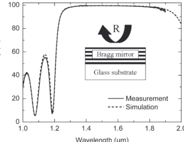
of four and a half period has been characterized by reflection measurement (Fig. 1). An experimental reflectivity near 99.5% has been measured with a spectral bandwidth of 800 nm. The stability of the Bragg mirror at RT has been verified for a long time (few months) and no variations of the reflectivity has been observed. The DBR mirror is also found to be very stable when it was annealed up to 240°C and stored. This stability of reflectivity with time and temperature allows us to use it with a metal bonding process. A VCSEL cavity has been realized with two a-Si/a-SiNx
Bragg mirrors using a metallic bonding method. A first a-Si/a-SiNx Bragg mirror, of five and a half periods has
been deposited on an InGaAsP based active region. First, the cavity and the DBR are bonded on a silicon substrate, the DBR is located at the bottom of the device (Fig. 2). InP substrate is removed by mechanical polishing and selective etching. Then, a second deposition of five periods of a-Si/aSiNx is realized to
obtain the front mirror of the VCSEL. As it is illustrated on Fig. 2, a good agreement is obtained between simulated and experimental reflectivity of the device. This result proves that the device has not been perturbed by the metallic bonding process. The VCSEL has been tested under optical pumping with a Q-switched YAG laser at 1.064 µm wavelength and shows lasing spectra at RT with an excellent spectral purity.
1 A. Karim, S. Björlin, J. Piprek, , and J. E. Bowers, IEEE J. of Selected Topics in Quantum Electron. 6, n° 6, (2000). 2 R. Shau, H. Halbritter, F. Riemenschneider, M. Ortsiefer, Electron. Lett. 39, n°24, (2003).
3 D. Sun, W. Fan, P. Kner, J. Boucart, IEEE Photon. Technol. Lett. 15, n°12, (2000).
Fig 1: Simulated and measured reflectivity for the DBR with a four and half periods of a-Si/a-SiNx