HAL Id: hal-01869960
https://hal.archives-ouvertes.fr/hal-01869960
Submitted on 7 Sep 2018
HAL is a multi-disciplinary open access
archive for the deposit and dissemination of
sci-entific research documents, whether they are
pub-lished or not. The documents may come from
teaching and research institutions in France or
abroad, or from public or private research centers.
L’archive ouverte pluridisciplinaire HAL, est
destinée au dépôt et à la diffusion de documents
scientifiques de niveau recherche, publiés ou non,
émanant des établissements d’enseignement et de
recherche français ou étrangers, des laboratoires
publics ou privés.
Silicon modulators for the generation of advanced
modulation formats
Diego Perez-Galacho, Laurent Bramerie, Charles Baudot, Mohamed Chaibi,
Sonia Messaoudène, Nathalie Vulliet, Laurent Vivien, Frédéric Boeuf,
Christophe Peucheret, Delphine Marris-Morini
To cite this version:
Diego Perez-Galacho, Laurent Bramerie, Charles Baudot, Mohamed Chaibi, Sonia Messaoudène, et
al.. Silicon modulators for the generation of advanced modulation formats. 20th International
Confer-ence on Transparent Optical Networks (ICTON 2018), Jul 2018, Bucharest, Romania.
�10.1109/IC-TON.2018.8473806�. �hal-01869960�
Silicon modulators for the generation of advanced modulation
formats
Diego Perez-Galacho1,2, Laurent Bramerie3, Charles Baudot4, Mohamed Chaibi3, Sonia Messaoudène4, Nathalie Vulliet4, Laurent Vivien2, Frederic Boeuf4, Christophe Peucheret3, Delphine Marris-Morini2
1ITEAM research institute, Universitat Politècnica de València, Camino de Vera s/n, 46022, Valencia, Spain 2Centre de Nanosciences et de Nanotechnologies, CNRS, Univ. Paris-Sud, Université Paris-Saclay, C2N-Orsay,
91405 Orsay cedex, France
3Univ. Rennes, CNRS, FOTON – UMR 6082, F-22305 Lannion, France 4STMicroelectronics, 850 rue Jean Monnet, 38920 Crolles, France
e-mail: [email protected]
ABSTRACT
Silicon photonics has appeared in the recent years as the best suited technology for fulfilling the demands of future optical interconnects. In this framework, modulators are key elements in the performance of an optical link. In order to achieve modulation in silicon the Free-Carrier Plasma Dispersion (FCPD) effect is normally used. In fact, silicon modulators based on carrier depletion have been demonstrated with outstanding performance up to 40Gbps. However, keeping up with bandwidth demands will require the use of more complex modulation formats like PAM4 or QPSK. At the same time, to avoid dispersion compensation circuits, the use of the O-Band (1260nm-1360nm) is preferred for short range optical communications. In this work we present our results on the generation of BPSK/QPSK signals using silicon modulators.
Keywords: Silicon modulators, silicon photonics, integrated optics, advanced modulation formats, coherent
optical communications.
1. INTRODUCTION
Silicon photonics technology has evolved enormously since the first demonstrations of active functionalities until nowadays high-performance transmitters and receivers [1-2]. The use of Si photonics in the long haul network, based on coherent optical communications will set a path for next industrialization of low cost and high performance optoelectronics transceivers [2]. Currently, standards are based on 100 Gbps transmission, however, growing bandwidth demands provoked by cloud based applications and multi-media will require new standards based on 200-400 Gbps [3]. Silicon based state-of-the-art OOK modulators are already reaching the 50 Gbps operation [4-5], nevertheless, scaling to higher bit rates require advanced modulation formats like PAM-n, QPSK or 16-QAM [6-12]. This was possible because the phase efficiency of the modulators has been significantly improved [13-14]. Even though the vast majority of these demonstrations have been carried out in C-Band of optical communications (around 1550nm), the use of the of the O-Band (around 1310nm) is normally preferred for short distance intra-data-center communications where silicon photonics based systems are being deployed [15]. Therefore, a lot of effort has been put to overcome the lower free carrier dispersion effect at the O-Band compared to the C-Band and high performance devices have been demonstrated, exhibiting low voltage operation or OOK modulation at 50 Gbps [16-17]. However, even higher bit rates will be required as the data exchanged inside data centers is continuously growing. For that reason, the development of higher modulation formats in the O-Band has been receiving increasing attention in the last years [18,9]. PAM-8 at 112 Gbps was demonstrated [9], however it is noticeable that QPSK modulator based on encoding data both in amplitude and phase has not been reported up to now in the O-Band.
The generation of QPSK signals is normally carried out using standard IQ modulators based on nested Mach-Zehnder Modulators [6], however a single dual-drive Mach-Mach-Zehnder modulator (DD-MZM) can be employed as a simpler way to generate it, reducing the power consumption of the transceiver [19]. This approach was fist demonstrated using LiNbO3 a modulator [20]. This approach offers key advantages for short distance intra data center communications like good power efficiency and scalability. In this work we report the first demonstration of QPSK signal generation using DD-MZM in silicon working in the O-Band. Operation at 20 Gbps is demonstrated with potential to scale data rate and spectral efficiency.
2. MODULATOR DESIGN
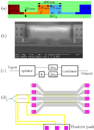
The silicon modulator designed was based on carrier depletion. We used phase shifters based on a PN diode embedded in the core of silicon-on-insulator (SOI) waveguide. In Fig. 1 (a) and (b) the schematic of the cross section and its SEM image are shown. The used phase shifter was based on a previously reported work demonstrating high modulation efficiency with VπLπ products of 0.95 to 1.15 Vcm for reverse bias from 1 to 4 V at 1310 nm wavelength [17]. The schematic of the DD-MZM is shown in Fig. 1 (c). A symmetric Mach-Zehnder structure is sued with 2 mm long phase-shifters embedded in both arms. MMI couplers implement the
input/output splitter and combiner. The biasing of the interferometer is carried out by tuning the DC phase shift Φ between both arms (see Fig. 1 (c)). This DC phase shift is actually implemented by metallic heaters that act as low-speed/high-efficient phase shifter, as shown in Fig. 1(d). The modulator was fabricated on the 300-mm CMOS DAPHNE technological platform of STMicroelectronics [21]. RF signals can be applied independently to each phase shifter by means of GSGSG coplanar traveling wave electrodes.
Figure 1. Cross section of the silicon phase-shifter: (a) schematic and (b) SEM image. Architecture of a DD-MZM: (c) schematic and (d) actual layout.
3. CHARACTERIZATION SETUP
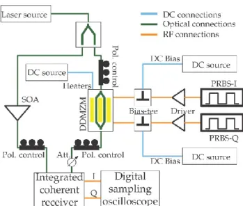
In Fig. 2 the characterization setup used to demonstrate QPSK modulation is shown. An O-Band external cavity laser was use to inject TE-polarized light in/out of the fabricated device by means of grating couplers. In order to drive electrically the phase shifters and the heaters, RF and DC electrical probes were used. The modulating signals were implemented using two 215-1 long de-correlated pseudo random binary sequence (PRBSs) at 10 Gbps. These two PRBSs modulating signal were amplified and DC biased prior to application to the modulator in order to ensure that the PN junctions operate in depletion. The final driving signals applied to the phase-shifters had a peak-to-peak voltage of 7Vpp and a DC bias of 4V. At the end of the GSGSG electrodes, loads were located to avoid reflected RF signals. DC tips were used to connect the heater and adjust the constant phase shift to bias the interferometer at a quadrature point (Φ=π/2). The modulated optical signal is then sent to a coherent receiver through a variable optical attenuator in order to adjust the received power. For the purpose of this first demonstration, the same laser was used at the transmitter and as local oscillator (LO) at the receiver, thus implementing homodyne detection. A semiconductor optical amplifier (SOA) was used to amplify the LO signal. The I/Q signals of the receiver were fed to a 40-GSps digital sampling oscilloscope (DOS) with 16-GHz electrical bandwidth. Blocks of 105 symbols were acquired and then processed offline. An adaptive finite impulse response (FIR) filter with decision-directed least mean square (DD-LMS) tracking was used as digital signal processing. The processed samples were used to obtain the constellation diagrams and to compute the bit-error-rate (BER). The BER was evaluated over five blocks of 105 symbols.
Figure 2. Experimental setup employed for QPSK signal characterization.
4. MEASUREMENTS RESULTS
Firstly the DD-MZM was characterized in DC. The obtained fiber-to-fiber transmission was 17 dB, this includes grating coupler loss, chip passive propagation loss and modulator insertion loss (IL). Normalizing by an on-chip straight waveguide of similar length, the IL of the modulator was calculated to be 3.8 dB. The measured Vπ of each phase shifter was between 6 V and 7V, considering the 2 mm active length of the modulator, the deduced modulation efficiency is between 1.2 Vcm and 1.4 Vcm. The small signal electro-optical 6-dB bandwidth of the modulator was measured around 15 GHz. QPSK operation at 10 Gbaud was then targeted.
Using the aforementioned setup high-speed measurements were performed on the DD-MZM. The bit error rate (BER) was measured as a function of the signal average received power, the resulting curve is shown in Fig. 3 (a). Five BER measurements were carried out for each received power point, therefore each point on Fig. 3 (a) is the result of averaging five measurements of 105 transmitted symbols each. Considering 10-3 as the limit in BER for error free transmission based on forward error correction, the required received power is -20dBm. The received constellation diagram after digital signal processing (DSP) performed offline can be seen in Fig. 3 (b), this constellation corresponds to a received power of -22 dBm. It can be observed a clear QPSK constellation, the corresponding error vector magnitude (EVM) for this constellation is 33%.
Figure 3. 3 BER as a function of the received power (a) and measured constellation diagram for a received power of -22dBm (b).
5. CONCLUSIONS
Intra data centers short-range optical communications based on the O-Band are nowadays facing important demands of bandwidth. Moving towards advanced modulation formats like PAM-n, QAM or QPSK will provide a solution in the short term. In this work, QPSK modulation in the O-Band using a silicon modulator has been proposed and demonstrated experimentally. Using a simple modulation structure based on a DD-MZM QPSK
data transmission is demonstrated at 10 Gbaud (20 Gbps) for the first time. The modulator of this demonstration benefits from requiring only two driving signals reducing the power consumption, a key parameter in short range communications.
ACKNOWLEDGEMENTS
This work was supported by the European projects Plat4m (FP7-2012-318178), Cosmicc (H2020-ICT-27-2015-688516) and BlueSpace (H2020-ICT-2016-2-762055). We acknowledge the support of French Industry Ministry/DGE through the Nano2017 program.
REFERENCES
[1] F. Boeuf, et al., “Silicon Photonics R&D and manufacturing on 300-nm wafer platform,” J. Lightw. Technol., vol. 34, no. 2, pp. 286-295, 2016.
[2] P. Dong, et al., “Silicon photonic devices and integrated circuits,” Nanophotonics, vol. 3, no. 4-5, pp. 215-228, 2014.
[3] J. Witzens, “Modulators make efficiency leap,” Nat. Photonics, vol. 11, pp. 459, 2017.
[4] P. Dong, et al., “High-speed low-voltage single-drive push-pull silicon Mach-Zehnder modulators,” Opt. Express, vol. 20, no. 6, pp. 1094-4087, 2012.
[5] D. J. Thomson, et al., “50-Gb/s Silicon Optical Modulator,” IEEE Photon. Technol. Lett., vol. 24, no. 4, pp. 234-236, 2012.
[6] P. Dong, et al., “112-Gb/s monolithic PDM-QPSK modulator in silicon,” Opt. Express, vol. 20, no. 26, pp. B624-B629, 2012.
[7] P. Dong, et al., “224-Gb/s monolithic PDM-16-QAM modulator and receiver based on silicon photonic integrated circuits,” in Optical Fiber Communication Conference/National Fiber Optic Engineers Conference 2013, pp. PDP5C.6.
[8] J. Ding, et al., “Silicon 16-QAM optical modulator driven by four binary electrical signals,” Opt. Lett., vol. 42, no. 8, pp. 1636-1639, 2017.
[9] M. Chagnon, et al., “Experimental study of 112-Gb/s short reach transmission employing PAM formats and SiP intensity modulator at 1.3µm,” Opt. Express, vol. 22, no. 17, pp. 21018-21036, 2014.
[10] A. Samani, et al., “Experimental parametric study of 128 Gb/s PAM-4 transmission system using a multielectrode silicon photonic Mach Zehnder modulator,” Opt. Express, vol. 25, no. 12, pp. 13252-13262, 2017.
[11] B. Milivojevic, et al., “Small-Size Silicon Photonic IQ Modulator and Low-Power CMOS Driver for Next Generation Coherent Transceiver,” in 18th European Conference on Network and Optical Communications & 8th Conference on Optical Cabling and Infrastructure, 2013, pp. 181-184.
[12] A. Shastri, et al., “Ultra-Low-Power Single-Polarization QAM-16 Generation Without DAC Using a CMOS Photonics Based Segmented Modulator,” J. Lightw. Technol., vol. 33, no. 26, pp. 1255-1260, 2015. [13] T. Hiraki, et al., “Heterogeneously integrated III-V/Si MOS capacitor Mach-Zehnder modulator,” Nat.
Photonics, vol. 11, no. 8, pp. 482, 2017.
[14] J.-H. Han, et al., “Efficient low-loss InGaAsP/Si hybrid MOS optical modulator,” Nat. Photonics, vol. 11, no. 8, pp. 486, 2017.
[15] T. Pinguet, et al., “Monolithically integrated high-speed CMOS photonic transceivers,” in 5th IEEE International Conference on Group IV Photonics, 2008, pp. 362-364.
[16] M. Streshinsky, et al., “Low power 50 Gb/s silicon traveling wave Mach-Zehnder modulator near 1300nm,” Opt. Express, vol. 21, no. 25, pp. 30350-30357, 2013.
[17] D. Perez-Galacho, et al., “Low voltage 25Gbps silicon Mach-Zehnder modulator in the O-band,” Opt. Express, vol. 25, no. 10, pp. 11217-11222, 2017.
[18] C. Xiong, et al., “Monolithic 56Gb/s silicon photonic pulse-amplitude modulation transmitter,” Optica, vol. 3, no. 10, pp. 1060-1065, 2016.
[19] C. R. Doerr, et al., “O, E, S, C and L Band Silicon Photonics Coherent Modulator/Receiver,” in Optical Fiber Communication Conference Postdeadline Papers 2016, pp. Th5C.4.
[20] K.-P. Ho and H.-W. Cuei, “Generation of Arbitrary Quadrature Signals Using One Dual-Drive Modulator,” J. Lightw. Technol., vol. 23, no. 2, pp. 764-770, 2005.
[21] C. Baudot, et al., “Daphne silicon photonics technological platform for research and development on wdm applications,” in Proc. SPIE 9891, 2016, pp. 98911D.