HAL Id: tel-01665199
https://tel.archives-ouvertes.fr/tel-01665199
Submitted on 15 Dec 2017
HAL is a multi-disciplinary open access
archive for the deposit and dissemination of sci-entific research documents, whether they are pub-lished or not. The documents may come from teaching and research institutions in France or abroad, or from public or private research centers.
L’archive ouverte pluridisciplinaire HAL, est destinée au dépôt et à la diffusion de documents scientifiques de niveau recherche, publiés ou non, émanant des établissements d’enseignement et de recherche français ou étrangers, des laboratoires publics ou privés.
Conducting Polymer Devices for in vitro
Electrophysiology
Dimitrios Koutsouras
To cite this version:
Dimitrios Koutsouras. Conducting Polymer Devices for in vitro Electrophysiology. Other. Université de Lyon, 2016. English. �NNT : 2016LYSEM017�. �tel-01665199�
N°d’ordre NNT : 2016LYSEM017
THESE de DOCTORAT DE L’UNIVERSITE DE LYON
opérée au sein del’Ecole des Mines de Saint-Etienne
Ecole DoctoraleN° 488 Sciences, Ingénierie, Santé Spécialité de doctorat : Bioélectronique
Discipline : Microélectronique
Soutenue publiquement à Gardanne le 30/09/2016, par :
Dimitrios A. Koutsouras
Titre de la thèse
Conducting Polymer Devices for in
vitro Electrophysiology
Devant le jury composé de :
BENFENATI, Valentina Professoressa a contratto UNIBO Présidente
IANNOTTA, Salvatore Professeur /Directeur de IMEM Rapporteur
LANG, Jochen Professeur CBMN Rapporteur
OWENS, Róisín Maître Assistante EMSE Examinatrice
SISKOS, Stylianos Professeur AUTH Examinateur
ABSI Nabil CR Génie industriel CMP
AVRIL Stéphane PR2 Mécanique et ingénierie CIS
BALBO Flavien PR2 Informatique FAYOL
BASSEREAU Jean-François PR Sciences et génie des matériaux SMS
BATTAIA-GUSCHINSKAYA Olga CR Génie industriel FAYOL
BATTON-HUBERT Mireille PR2 Sciences et génie de l'environnement FAYOL
BERGER DOUCE Sandrine PR2 Sciences de gestion FAYOL
BIGOT Jean Pierre MR(DR2) Génie des Procédés SPIN
BILAL Essaid DR Sciences de la Terre SPIN
BLAYAC Sylvain MA(MDC) Microélectronique CMP
BOISSIER Olivier PR1 Informatique FAYOL
BONNEFOY Olivier MA(MDC) Génie des Procédés SPIN
BORBELY Andras MR(DR2) Sciences et génie des matériaux SMS
BOUCHER Xavier PR2 Génie Industriel FAYOL
BRODHAG Christian DR Sciences et génie de l'environnement FAYOL
BRUCHON Julien MA(MDC) Mécanique et ingénierie SMS
BURLAT Patrick PR1 Génie Industriel FAYOL
COURNIL Michel PR0 Génie des Procédés DIR
DAUZERE-PERES Stéphane PR1 Génie Industriel CMP
DEBAYLE Johan CR Image Vision Signal CIS
DELAFOSSE David PR0 Sciences et génie des matériaux SMS
DELORME Xavier MA(MDC) Génie industriel FAYOL
DESRAYAUD Christophe PR1 Mécanique et ingénierie SMS
DOLGUI Alexandre PR0 Génie Industriel FAYOL
DRAPIER Sylvain PR1 Mécanique et ingénierie SMS
FAVERGEON Loïc CR Génie des Procédés SPIN
FEILLET Dominique PR1 Génie Industriel CMP
FRACZKIEWICZ Anna DR Sciences et génie des matériaux SMS
GARCIA Daniel MR(DR2) Génie des Procédés SPIN
GAVET Yann MA(MDC) Image Vision Signal CIS
GERINGER Jean MA(MDC) Sciences et génie des matériaux CIS
GOEURIOT Dominique DR Sciences et génie des matériaux SMS
GONDRAN Natacha MA(MDC) Sciences et génie de l'environnement FAYOL
GRAILLOT Didier DR Sciences et génie de l'environnement SPIN
GROSSEAU Philippe DR Génie des Procédés SPIN
GRUY Frédéric PR1 Génie des Procédés SPIN
GUY Bernard DR Sciences de la Terre SPIN
HAN Woo-Suck MR Mécanique et ingénierie SMS
HERRI Jean Michel PR1 Génie des Procédés SPIN
KERMOUCHE Guillaume PR2 Mécanique et Ingénierie SMS
KLOCKER Helmut DR Sciences et génie des matériaux SMS
LAFOREST Valérie MR(DR2) Sciences et génie de l'environnement FAYOL
LERICHE Rodolphe CR Mécanique et ingénierie FAYOL
LI Jean-Michel Microélectronique CMP
MALLIARAS Georges PR1 Microélectronique CMP
MAURINE Philippe Ingénieur de recherche Microélectronique CMP
MOLIMARD Jérôme PR2 Mécanique et ingénierie CIS
MONTHEILLET Frank DR Sciences et génie des matériaux SMS
MOUTTE Jacques CR Génie des Procédés SPIN
NEUBERT Gilles PR Génie industriel FAYOL
NIKOLOVSKI Jean-Pierre Ingénieur de recherche CMP
NORTIER Patrice PR1 SPIN
OWENS Rosin MA(MDC) Microélectronique CMP
PICARD Gauthier MA(MDC) Informatique FAYOL
PIJOLAT Christophe PR0 Génie des Procédés SPIN
PIJOLAT Michèle PR1 Génie des Procédés SPIN
PINOLI Jean Charles PR0 Image Vision Signal CIS
POURCHEZ Jérémy MR Génie des Procédés CIS
ROBISSON Bruno Ingénieur de recherche Microélectronique CMP
ROUSSY Agnès MA(MDC) Génie industriel CMP
ROUSTANT Olivier MA(MDC) Mathématiques appliquées FAYOL
ROUX Christian PR Image Vision Signal CIS
STOLARZ Jacques CR Sciences et génie des matériaux SMS
TRIA Assia Ingénieur de recherche Microélectronique CMP
VALDIVIESO François PR2 Sciences et génie des matériaux SMS
VIRICELLE Jean Paul DR Génie des Procédés SPIN
WOLSKI Krzystof DR Sciences et génie des matériaux SMS
XIE Xiaolan PR1 Génie industriel CIS
YUGMA Gallian CR Génie industriel CMP
BERGHEAU Jean-Michel PU Mécanique et Ingénierie ENISE
BERTRAND Philippe MCF Génie des procédés ENISE
DUBUJET Philippe PU Mécanique et Ingénierie ENISE
FEULVARCH Eric MCF Mécanique et Ingénierie ENISE
FORTUNIER Roland PR Sciences et Génie des matériaux ENISE
GUSSAROV Andrey Enseignant contractuel Génie des procédés ENISE
HAMDI Hédi MCF Mécanique et Ingénierie ENISE
LYONNET Patrick PU Mécanique et Ingénierie ENISE
RECH Joël PU Mécanique et Ingénierie ENISE
SMUROV Igor PU Mécanique et Ingénierie ENISE
TOSCANO Rosario PU Mécanique et Ingénierie ENISE
ZAHOUANI Hassan PU Mécanique et Ingénierie ENISE
EMSE : Enseignants-chercheurs et chercheurs autorisés à diriger des thèses de doctorat (titulaires d’un doctorat d’État ou d’une HDR)
ENISE : Enseignants-chercheurs et chercheurs autorisés à diriger des thèses de doctorat (titulaires d’un doctorat d’État ou d’une HDR) Spécialités doctorales Responsables :
SCIENCES ET GENIE DES MATERIAUX K. Wolski Directeur de recherche
MECANIQUE ET INGENIERIE S. Drapier, professeur
GENIE DES PROCEDES F. Gruy, Maître de recherche
SCIENCES DE LA TERRE B. Guy, Directeur de recherche SCIENCES ET GENIE DE L’ENVIRONNEMENT D. Graillot, Directeur de recherche
Spécialités doctorales Responsables
MATHEMATIQUES APPLIQUEES O. Roustant, Maître-assistant
INFORMATIQUE O. Boissier, Professeur
IMAGE, VISION, SIGNAL JC. Pinoli, Professeur
GENIE INDUSTRIEL A. Dolgui, Professeur
MICROELECTRONIQUE S. Dauzere Peres, Professeur
Mi se à jo ur : 29/ 06 /20 15
Table of Contents
Acknowledgments ... 1
Chapter 1: Introduction ... 4
1.1 Bioelectronics – Organic Devices ... 4
1.2 Organic Electronics Fabrication Processes... 6
1.2.1 Photolithography ... 8
1.2.2 Basic principles... 9
1.2.3 Fabrication steps ... 11
Substrate cleaning ... 11
Deposition of the photoresist ... 12
Post-apply bake... 14
Use of the mask/alignment/exposure ... 15
Development ... 17
Descumming and postbaking... 17
Pattern transfer ... 18
Stripping ... 19
1.2.4 Photolithography in polymer device fabrication ... 20
Sacrificial layer methods ... 20
Orthogonal photoresist method ... 24
1.3 Concepts of Neuroscience ... 27 1.3.1 Neurons ... 27 1.3.2 Glia ... 30 1.3.3 Action Potential ... 31 1.4 Concepts of Electrophysiology ... 33 In vitro electrophysiology ... 34 References ... 38
Chapter 2: Biopotential Electrodes ... 40
2.1 Introduction ... 40
2.2 Theoretical model of the neural recording ... 43
2.3 Conducting Polymer Coated Electrodes ... 46
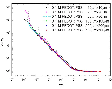
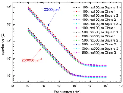
2.4 Impedance Spectroscopy of PEDOT: PSS Coated Electrodes as a Function of Area ... 49
2.5 Electrodeposition ... 61
2.6 Conclusions ... 65
References ... 67
Chapter 3: In vitro PEDOT:PSS Microelectrode Arrays for hippocampal cell culture electrophysiological recordings ... 68
3.1 Abstract ... 68
3.2 Experiment-Results ... 69
3.3 Conclusions ... 77
3.4 Experimental Section ... 77
3.4.1 Microelectrode Arrays fabrication: ... 77
3.4.2 Preparation of the rat hippocampal cell cultures: ... 78
3.4.3 Electrical and electrophysiological recordings: ... 78
References ... 80
Supplementary Information ... 81
Chapter 4: A PEDOT:PSS in vitro Platform for Pancreatic Islet Cell Electrophysiology ... 84 4.1 Abstract ... 84 4.2 Experiment – Results ... 85 4.3 Conclusions ... 93 4.4 Experimental Section ... 94 4.4.1 Device Fabrication ... 94
4.4.2 Islets isolation and cell culture ... 95
4.4.3 Device characterization and electrophysiological recordings ... 95
References ... 96
Supplementary Information ... 97
Chapter 5: Organic Electrochemical Transistors ... 99
5.1 Introduction ... 99
5.2 Organic Electrochemical Transistors measuring system ... 103
5.3 Conclusions ... 111
References ... 112
Chapter 6 Organic Electrochemical Transistor for Astrocytes activity recordings ... 113
6.1 Introduction ... 113
6.2 Experiment- Results ... 114
6.2.2 Device characterization in external standard solution ... 114
6.2.3 Recordings of astrocytes’ activity using OECT ... 116
6.2.4 OECT astrocytes recordings using pharmacological inhibitor and ATP .. 117
6.2.5 OECT Astrocytes recordings during calcium microfluorimetry ... 118
6.3 Conclusions ... 119
6.4 Experimental Section ... 120
6.4.1 Cell viability assay: ... 120
6.4.2 Device Fabrication: ... 120
6.4.3 Biological measurement: ... 121
6.4.4 Calcium microfluorometry: ... 121
References ... 122
Supplementary Information ... 123
Chapter 7: Conclusion – Outlook ... 124
Appendix A: Noise characterization and modeling ... 127
Appendix B: Spreading resistance Rs ... 133
Appendix C: List of Abbreviations ... 137
1
Acknowledgments
It is often argued that the 3 years of the PhD studies is a special period in every student’s life. I think this cannot be truer in my case. I am not sure if those have been the best three years in my life but I am absolutely sure that are the years that marked me the most and will follow me forever. Those are the years that has changed me as a person (hopefully made me grow more mature) and that is why I will always recall my time in France full of emotions and memories.
To begin with, I would like to thank my advisor Professor George G. Malliaras for offering me the opportunity to come, study and work in the Department of Bioelectronics in Gardanne under his supervision. First, I would like to thank him for his trust, his guidance, his support and his encouragement these 3 years. I would also like to thank him for introducing me to the way research in a high scientific level is done and for being a continuous source of inspiration during my project. Foremost, I would like to thank him because he is the reason of me being in this scientific field making a turn in my carrier. If it was not for him there is no way I could have followed my dreams and this is why I shall be forever in his debt.
I am especially thankful to Professor David C. Martin for his guidance and his support. Luckily for me, my time in BEL co-existed with his Sabbatical time in our lab. The result was a project on the effect of electrodes area in their impedance Spectra and countless hours of fruitful scientific, and not, conversations. I am also grateful to Professor Eric di Pasquale who was the man to provide me with beautiful hippocampal cell cultures exactly the moment I needed them the most in order to finish my project. He was the one who introduced me to the world of electrophysiology and we spend many hours together talking about science and philosophy. Of course, our relationship has evolved to something more than a professional one and I would like to consider him as one of my friends.
I would also like to thank Assistant Professor Roisin Owens who, with her knowledge in biology, her will to offer help at any time and her guidance, made my work life much easier. I am also thankful to Professor Stylianos Siskos with whom we
2
run a project that I am sure it will pay off very soon. I strongly believe that read out system that was designed will allow the OECTs to fulfil their true potential.
My special thanks go to Professor Jochen Lang who gave me the opportunity to experiment the use of organics to cells other than neurons and to broaden my electrophysiological horizons to pancreas cells and to Valentina Benfenati who hosted me for a month in her lab in Bologna and gave me the opportunity to work with astrocytes. The four above along with Professor Salvatore Iannotta are the members of my jury and I would like to thank them for reading and correcting my thesis.
I would also like to thank all the PhD students, Post docs and P.I.s involved in OLIMPIA project. Every OLIMPIA meeting was a great opportunity for scientific discussions and lots of fun!
During my PhD studies I was lucky enough to supervise three master students. Maria Villiou, Petros Sideris and Clemens Stolz. I cannot thank them enough for their help and for the fact that I also learned from them maybe even more than I taught them!
Many thanks go to Eileen Pedraza, Romain Perrier, Ariana Villarreal and to Assistant Professor Matthieu Raoux from CBMN UMR-CNRS in Bordeaux and to Simone Bonetti, Ana Borrachero from CNR-ISMN in Bologna for their help during the projects we run together.
The number of people from BEL that I would like to thank are way more than those that I can fit in a couple of pages. So I would like to thank, from the bottom of my heart, all the people that I met, worked with and had fun with during these 3 years of my presence in the department of bioelectronics. Thank you all for the memories! I really appreciate what you did for me!
Special thanks go to Jolien Pas and Adel Hama for their help in the neuron recording project and to Anton Ivanon from Institut de Neurosciences des Systèmes of Aix-Marseille University for introducing me to electrophysiology. Special thanks also go to the technicians of the clean room, to the employees at CMP for their help and particularly to Sabine Salmeron for giving me “shelter” in the library and teaching me French. I also thank my former supervisor Professor Stergios Logothetidis as I owe
3
him my presence in France and my friends and relatives back in Greece for never forgetting me.
It is very difficult to describe how much grateful I feel to postdoc Paschalis Gkoupidenis. It is not only the fact that he taught me how to do scientific research. He also changed my mentality and gave me guidance when I needed it the most. Paschalis is not only one of the best colleagues I have ever had, he is also a true friend and I am extremely lucky to have met him.
Last but not least, I would like to thank my family. I do not think there is any word that can express my gratefulness towards them. My father Thanasis , my mother Spyridoula and my brother Nikos have been always there for me and I do not think I would have made it without them. Of course, I am also grateful to Athina for her love and her support. Above all, I want to apologize to all of them for the pressure I was putting on their shoulders when my problems were, so unfairly, affecting their lives and to thank them for putting up with me. Thank you from the bottom of my heart!
Dimitrios A. Koutsouras September 2016
4
Chapter 1: Introduction
1.1
Bioelectronics – Organic Devices
Bioelectronics is the field of science that tries to merge two very different worlds .The world of Biology and the one of Electronics. The motivation behind such an effort is, obviously, the continuous need to find better ways of interaction between electronic devices and living tissue both in fundamental research level but also in diagnostics and therapeutics.
The problems start the moment we realize the fundamental differences between the two systems. Conventional electronics are made, mostly, out of silicon which is a tough and rigid material held together by a network of covalent bonds. Furthermore, they are solid and conduct charge with electrons and holes. Biological matter, on the other hand, is “soft”, wet and conduct charge by ion transport. These differences in the materials’ structure and properties are the reason behind a problematic matching that needs to be taken into account for any transducer functioning between biotic tissue and abiotic medical devices [1, 2].
Organic electronics came into light as the new way to bridge this mismatch and to offer alternative interfacing approaches. The term “Organic Biolectronics”,in particularly, was firstly introduced by Magnus Berggren and Agneta Richter-Dahlfors in 2007 in a seminal review[3] describing this new research approach.
Long before that , Organic electronics had attracted the increasing interest of the scientific community mostly due to their synthetic tunability, their electronic properties and their low temperature processing[1]. By definition, organic electronics refers to the use of carbon based semiconductors either as conjugated small molecules or as conjugated polymers. Especially for the case of conjugated polymers by the end of 1970s Heeger et al, demonstrated that acetylene can become highly conducting when doped with iodine[4] (Nobel Prize in Chemistry 2000). The 1980’s was the decade of blossom of organics in electrophotography and by the end of the decade the first organic light emitting diode (OLED) was produced[5]. Naturally, during 1990’s OLEDs, organic thin film transistors (OTFTs) and organic photovoltaics (OPVs) where intensively studied resulting in their extensive commercialization.
5
The real question is, though, whether organic electronics can provide any significant advantage in comparison to the existing silicon technology in the field of bioelectronics or not.
There are a couple of reasons that support organics potential to revolutionize the field and they can be summarized as follow. First, it is the mechanical properties of conducting polymers that distinguish them from their inorganic counterparts. Organic electronic materials are “soft” to their nature, a fact that gives them better mechanical compatibility to tissue and to flexible substrates that very commonly are used as implantable devices. Second, they support mixed ionic/electronic conductivity. This is a tremendous advantage since living tissue communicates through ion movement while solid electronics communicate through electrons and holes. Conjugated polymers can bridge this gap by speaking both languages. Third, the weak van der Waals bonding of organics results in dangling and oxide free interfaces with aqueous electrolytes. This is translated into a direct contact between the sensing/recording device and the biomoiety offering better, more direct and cleaner interaction. Last, but not least, polymers provide freedom in chemical modification. This means the whole arsenal of organic chemistry is available for modifications in the polymer chain which result in an increased biological functionality[1, 2].
Consequently, the term organic bioelectronics obtains a completely new meaning. It reflects a new effort of coupling electronic devices and biological objects; a coupling that is not only extremely advantageous but also work in a bilateral way. In one direction, a biological process creates a signal to an organic device; for example an enzymatic reaction (glucose oxidation) causes the current in an Organic Electrochemical Transistor to change (glucose sensing). In the other direction, an organic electronic device causes a biological phenomenon to occur; voltage applied through a polymer covered stimulates a neuron to fire action potentials (Figure 1.1).
6
Figure 1.1: The two way coupling between organic electronic devices and biology[1]. For the reasons above, organic electronics seems to be the ideal candidate for allowing bioelectronics to fulfil its true potential. That does not mean that organic electronics are here to replace existing silicon technology but rather that they can act complementary to it by offering a novel toolbox for interfacing with biology.
Next we are going to focus a bit on the organic electronics device fabrication process as it poses a number of challenges which inevitably come hand to hand with the conducting polymer special nature.
1.2
Organic Electronics Fabrication Processes
As extensively presented in the previous part, during the past decades the field of Organic Electronics has attracted the increasing attention of the scientific community as an attempt to complement traditional silicon electronics and to broaden their horizons[6]. There are a number of good reasons justifying this trend as organic materials present a unique set of properties. In particularly, they allow fabrication of thin, flexible, lightweight, environmental friendly and low cost devices[7]. Moreover, they offer ease of processability, low temperature solution-based deposition, and the degree of freedom that comes with their chemically tunable properties[8].
Nevertheless, before this new emerging technology becomes mature enough to influence the electronic industry, the major issue of organic film patterning must be addressed. There is an inextricable link between electronic device performance and
7
electronic material patterning and that is the reason why many different methods have been developed throughout the past years to optimize the fabrication process. Especially when it comes to organics, patterning is a challenging task as the technique of choice should be compatible with their special nature.
Unfortunately, despite its comparative advantages, conventional photolithography lacks compatibility with the vast majority of organic electronic materials. This is due to the fact that solvents used during deposition, development, and removal of photoresists have, in most cases, adverse effect on organic films. As a result, the already existing and well-developed industry of conventional silicon-based electronics can only provide limited tools for organics electronics[9]. Thus, the goal of overcoming those incompatibilities is of great importance as it will allow the use of the accumulated knowledge of an already well established and commercially successful fabrication approach.
In contrast, other nondestructive patterning techniques employed throughout the past years did not manage to live up to their potential. Vapor deposition through shadow masks, soft and hard imprint lithography, thermal transfer process and laser assisted printing were originally introduced as alternative approaches promising a convenient and easy way of device fabrication. Nevertheless, all these techniques suffer from numerous drawbacks. In particular, shadow mask deposition is the technique of choice for small-molecule patterning but lacks the ability of high resolution fabrication. Imprint technology on the other hand can offer resolution down to 10nm but it can be used only with a limited number of materials and device architectures[10].In addition all of the above techniques have issues with low resolution, poor scalability to larger areas, lack of registration and the fact that they tend to follow complex and costly processing protocols[11]. These disadvantages render them unable to compete with today’s state of the art fabrication processes.
In this part of the thesis we introduce novel approaches for conducting polymer device fabrication. In particular, what we are interested in is high throughput, cost effective and simple fabrication techniques, applicable to polymers and able to reproducibly create organic devices with high yield and efficiency. That is why we focus on polymer-friendly photolithography.
8 1.2.1 Photolithography
The term photolithography is a compound word made up from the Greek words Photo (Φως=light), litho (λίθος=stone) and graphy (γραφή=writing). As implied by its name, Photolithography is the process of transferring (writing) a pattern onto a substrate with the help of light.
Going back in time, there are two main landmarks in the development of photolithography. The first is the experiments of the Swiss pastor Jean Senebier (1742-1808) of Geneva with resins, in 1782. Senebier noticed that certain resins become insoluble in a solvent (turpentine) after sunlight exposure. The second pivotal moment comes with the work of Nicéphore Niépce on photography in 1826. Niépce, inspired by Senebier, was the first one to produce an image using the properties of light in Chalon (France). He used bitumen of Judea (a form of asphalt) dissolved in lavender oil, to coat a pewter plate and then he covered it with an etched print on oiled paper. The latter would serve as a mask for the three hours exposure to sunlight which was to follow. During this time, the exposed parts of the resist became insoluble while the protected ones could easily be removed by a mixture of turpentine and lavender oil corresponding to a photoresist behavior classified later as negative. Nevertheless, the first photolithography pattern transfer took place five years later, in 1827, by the Parisian engraver Augustin Francois Lemaître. Lemaître used a strong acid to etch a Niépce plate and to create a copy of a gravure of Cardinal d’Amboise, employing for the first time both photolithography and the chemical etching technique in a pattern transfer[12, 13].
Photolithography gradually became popular between the members of the scientific community as many of them started to realize the potential of the new technique. A little more than 100 years later, William Shockley and his co-workers at Bell Laboratories wanted to use photolithography for the fabrication of the first integrated circuit. However the need for a photoresist that could withstand the hydrofluoric etching of silicon dioxide (an important feature for their microfabrication process) made them turn to Kenneth Mees, Director of the Eastman Kodak Laboratories at Rochester New York. Mees contacted Louis Minsk, who in 1935 developed the first synthetic photopolymer known as poly(vinyl cinnamate), the basis of the first negative photoresist. His idea relied on the photoresist becoming less soluble upon exposure to light. Misk used that feature in order to define which part of
9
the photoresist would dissolve and which would remain on the substrate. In his approach the dissolved parts would be the ones to create the desired pattern. Five years later, in 1940, Oskar Süß developed a positive photoresist (diazonaphthoquinone)[13] which worked in the opposite way with the pattern formed by the part of the photoresist that remains after exposure to light.
Today, many more chemical substances have been synthesized, characterized and used in photolithography both as negative and positive photoresists. At the same time, optimization and variation of radiation sources in lithography and (X-ray lithography, charged particles lithography etc.) allow the patterning with nanometric resolution. The comparison with the 0,5-1mm accuracy achieved by Lemaître during the first photolithographic attempt shows the extent of progress[12].
1.2.2 Basic principles
The basic principle behind photolithography is the use of light in order to alter the solubility of a thin film that is exposed to it. A mask is a stencil, usually made out of chromium, that protects selected parts of the photosensitive material while the uncovered ones undergo changes in their properties (solubility) during the exposure. After immersion into a developer, the parts that became more soluble are dissolved leaving the desired pattern on the film behind. It is obvious that the photosensitive material plays a key role in the success of the process. This material is typically an organic polymer, called photoresist, which can go through a series of photochemical reactions when exposed to light.
It should also be noted that the term Photolithography usually refers to the use of ultra violet light (UV- wavelengths 436nm and 365nm) during patterning. Nevertheless, deep ultraviolet (DUV- wavelengths 248nm and 193nm) and extreme ultraviolet (EUV- wavelengths 5-100nm) photolithography techniques are both feasible and appealing, as in theory when the wavelengths of the light sources diminish the feature resolution increases. Nevertheless, it is difficult to find light sources with enough output power, the proper photoresists and the optical elements[14] for those short wavelengths. Moving a step further, X-Ray lithography, charged particle lithography or atomic force microscopy (AFM) lithography promise even better resolution, posing at the same time extra technological challenges. In this
10
chapter every time we use the term Photolithography it will be implied that we refer to UV Photolithography.
Returning to photoresists, they can roughly be divided into two categories. Positive photoresists (positive tone) and negative ones (negative tone). A positive photoresist is a photoresist which, when exposed to light, changes chemically and/or structurally becoming more soluble to an organic developer while, ideally, it was insoluble before. The mechanism behind this transformation can be either a polymer chain scission (e.g. poly(methylmethacrylate)- PMMA photoresist) or a photo induced change in the polarity of the molecule (e.g. two components DNQ-phenolic novolac resin)[12, 15]. A negative photoresist works in the exact opposite way. The photoresist is soluble to the developer and exposure to UV light either promotes polymeric cross-linking or starts the polymerization of the monomers. That renders the exposed photoresist insoluble to the developer, hence unexposed parts of the film are removed during the development step that follows. Common negative tone photoresists are the two-component bis(aryl)azide rubber resists (Kodak KTFR- azide-sensitivity poly(isoprene) rubber)[12, 15].
For both these types of photoresists the exposure, the development and the final pattern formation on the substrate is depicted in Figure 1.2.
11
In general, positive photoresists are more expensive than the negative ones but can offer higher resolution. This feature, along with the fact that positive photoresists can be developed in less toxic water based developers, made them more popular than the negative in industry. Nevertheless, many steps forward have been made lately in the synthesis and development of new negative resists. As a result, the newer negative tone resists are water developable and can also offer high resolution[12]. In addition, negative photoresists traditionally adhere better on substrates and they are more resistant to wet or dry etching than positive ones[12]. In conclusion, the choice of the proper photoresist depends on many different parameters (cost, resolution, pattern geometry etc.) all of which need to be taken into account before a decision is made.
Nowadays, photolithography is the most popular technique of patterning in the Integrated Circuits Industry. It offers a reliable and reproducible way of building up electronic devices with great accuracy and high resolution. Its main disadvantage is the limitations in the topography as it can only be implemented on planar substrates. The process performance can be evaluated through three figures of merit:
Resolution: It is a measure of the minimum size of a feature that can be patterned. It needs to be as high as possible in order for the feature size to be small
Registration: It is a measure of how accurately patterns on different layers can be aligned with respect to each other.
Throughput: It is the number of substrates that can be exposed per hour. The higher the throughput the more efficient the process.
1.2.3 Fabrication steps
The typical fabrication steps that take place during microfabrication are briefly reviewed below.
Substrate cleaning
The first, but definitely one of the most important steps in device fabrication is substrate cleaning. There are several different types of substrates that can be used for electronic circuit development. Silicon wafers are very common, especially in silicon-based semiconductor industry, but other kinds of substrates may also be employed.
12
Glass slides, conformable substrates (like Parylene-C) or even less conventional substrates as textiles and silk are among them. Despite the fact that some of those substrates may have special requirements or even incompatibilities with the standard cleaning protocols, the cleaning step cannot be easily omitted. Keeping the substrate free of contaminants is a matter of great importance as the degree of its cleanness affects the quality of the deposited film. Moreover, particles on the substrate could potentially lead to damage of the photomask during contact photolithography exposure (Figure 1.3) or even cause, in some cases, undesirable masking effects due to light diffraction. Among the contaminants that should be removed before coating the substrate with photoresist are atmospheric dust from operators and equipment, organic particles, moisture, H2O residue films, solvent stains, smoke particles,
residual resist, particulates and chunks of granular matter[12, 16].
The cleanliness of the fabrication environment is of critical importance hence all fabrication steps take place in a clean room environment (typically class 100) which allows the presence of up to 100 particles (sized 0.5μm or larger) per cubic foot of atmosphere. An environment like this minimizes the amount of unwanted particles in the milieu and a result minimizes the number of unwanted contaminants on the device as well. Taking this environment as granted, typical cleaning procedures may include both wet and dry methods. Sonication in water soap baths or solvent baths are normally employed for the removal of particles (both inorganic and organic). In some cases piranha solution (a 3:1 mixture of sulfuric acid and hydrogen peroxide) can also be used for organic particles detachment. Additional approaches include thermal treatment at high temperature (dehydration bake), plasma cleaning, vapor cleaning and supercritical cleaning with CO2 during which supercritical fluid of carbon dioxide
is used for removal of inorganic and organic contaminants from cracks and clefts due to its ability to penetrate into crevices. [12, 16, 17].
Deposition of the photoresist
Once substrate cleanliness is ensured, deposition of the photoresist on the substrate follows. Among the ways of depositing polymers on a substrate spin coating is the one which can guarantee uniformity, reproducibility and precision during deposition. It is a well-known, traditional technique which is rather easy to use and
13
offers control of the film thickness. The main drawback is the fact that the majority of the processed material is wasted.
Consequently, spin coating deposition has been the method of choice for photoresist thin film formation during fabrication for several decades now. During this approach, a small droplet of the photoresist is placed in the middle of the substrate which is secured on a chuck via vacuum. Centripetal acceleration spreads the photoresist on the substrate. Although almost 98% of the initial material is wasted, eventually a thin film of photoresist is deposited on the substrate. (Figure 1.3)
Figure 1.3: (a) Photoresist is placed on the substrate. (b) Film formation due to centripetal acceleration.
Thickness h of the photoresist is controlled through specific parameters of the process. Angular spinning speed ω and time t as well as the liquid density ρ, material viscosity η and evaporation rate ee are the most important factors affecting film’s
formation. During this process complex non-equilibrium phenomena take place and it is believed that two parts contribute to the rate by which the thickness of the film changes over time. A part that refers to the effect of the angular spinning speed and a part connected to the evaporation rate of the photoresist ee. Generally the spinning
cycle can be separated into two stages: a very fast coating stage (when the photoresist is spread on the substrate) and a longer drying stage (during which the solvent evaporates). In any case, the rheology behind the film formation is rather complex especially if the evaporation of the photoresist is taken into account. Therefore, the film thickness is usually given by the empirical expression (1)[12, 16, 17] :
14 ℎ =𝐾 𝐶𝛽𝜂𝛾
𝜔𝛼 (1)
where K is an overall calibration constant, C is the polymer concentration in g/100mL and η is the solution’s viscosity. The exponential parameters α, β and γ are determined experimentally. Once these parameters are set, a calibration curve is obtained which can provide the film thickness for a given polymer and solvent. Usually, film thickness is inversely proportional to the square root of the angular spinning speed ω and proportional to the solutions viscosity η to the 0.4-0.6 power[17].
ℎ ∝𝜂0.4−0.6
√𝜔 (2)
There are two common ways to realize photoresist’s dispersion on the substrate: the static dispense and the dynamic dispense. During the static dispense a small droplet of photoresist is deposited on the substrate while it is immobile. The amount of material deposited is in direct correlation with the viscosity of the photoresist (more viscous photoresists need more material to be placed) and the size of the substrate (bigger substrates need more material for the total coverage of the substrate to be ensured). On the other hand, dynamic dispersion dictates an initial step of spinning at a low speed (typically 500 rpm) while the dispense takes place. After that the substrate is accelerated to its final speed. Theoretically, this approach facilitates the wetting of the substrate the spreading of the material and consequently the film formation especially in the case of photoresists with poor wetability. [12, 17,
18]
..
For both approaches the angular spinning speed and the time of the spinning are the two parameters that affect the final thickness of the film. In general high speed and longer spinning times end up in thinner film formation.
Post-apply bake
What follows is a thermal treatment step called post-apply bake (PAB) (or soft bake). It usually lasts for a minute or two on a hot plate at 110oC. The purpose of this step is to evaporate the remaining solvent from the photoresist and to densify it just before exposure. That renders the coated film more stable and reduces the probability of the covered substrate to stick on the mask during exposure.
15 Use of the mask/alignment/exposure
Exposure stands at the very heart of the fabrication process. The basic principle behind photolithography, after all, is altering a photoresist’s solubility by delivering energy to it via radiation. The stencil that is used to transfer the desired pattern on the photosensitive film is called the “mask”. Generally a mask is made of glass (transparent to UV radiation) with a metal pattern on it (usually it is used a 800 Å Chromium film). The glass windows allow the radiation to pass through it with very little absorption while the metal pattern protects the underlying photoresist from any interaction with light. Masks are constructed with electron beam lithography which can result in higher resolution than photolithography[12]. Special care is also taken in the proper alignment of different device layers to each other during the exposure. As previously stated this is one of photolithography’s figure of merit (Registration) and is handled with the use of special marks (alignment marks) strategically placed on the different layers[14]. After all, registration is one of the main of the advantage of photolithography compared to the rest of the techniques along with its high throughput due to its parallel nature.
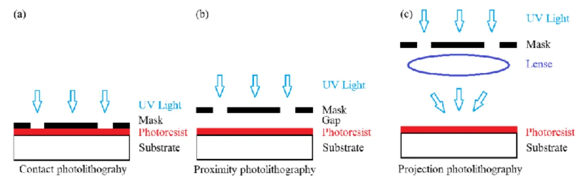
There are three different ways to perform the exposure: Contact, Proximity and Projection mode as shown in Figure 1.4.
Contact mode
Contact mode lithography was the first mode to be used in the early 1960s. In this approach the substrate is in physical contact with the mask during the exposure. The alignment of the substrate is made, yet, with the creation of a temporal gap between the two. The resolution of contact printing is rather high as it can go down to the wavelength of the radiation. Nevertheless, the high risk of mask damage due to the contact with the substrate motivated a search for alternative modes of photolithography.
16 Proximity mode
Here mask and substrate are not in contact anymore as there is a small gap (10-50μm) between the two. That protects the mask from damage but at the same time lowers resolution due to diffraction effects.
Contact and proximity mode printing are known together as shadow printing. The resolution r for them is given by the formula [14, 16, 17]:
𝑟 =3
2√𝜆 (𝑠 + 𝑑
2) (3)
where λ is the radiation wavelength, s is the distance between the mask and the substrate and d is the photoresist thickness
Projection mode
This is the mode of choice used in semiconductor industry from the mid-1970s to today. In projection printing, there is no direct contact between the mask and the substrate as the mask is projected onto the substrate through a lens system. This approach protects the mask from damage since there is no physical contact involved. In addition, the demagnification of the mask pattern achieved with the optics results in high resolution and makes the mask fabrication a little easier[12].
Figure 1.4: Schematic representation of the three exposing modes. (a) Contact photolithography. (b) Proximity Photolithography. (c) Projection mode.
The resolution r for projection printing is given by [14, 16, 17] : 𝑟 = 𝑘 𝜆
17
where k is a coefficient that depends on process-related factors and NA is the numerical aperture.
Development
After exposure, a development step will allow the latent resist pattern formed to be revealed. A selective dissolution creates a relief that will serve as a mold for the next fabrication steps. Development is of extreme importance as it controls the quality of the transferred motif.
There are two main approaches to perform this step: wet development and dry development.
Wet development
In wet development aqueous and organic solvents are used to dissolve selectively the exposed photoresist. Positive photoresists are developed in aqueous alkaline solutions while negative photoresists are developed in organic solutions. Aqueous development is preferable for environmental reasons and that is why newer negative resist may also be developed in aqueous solutions[12]. The aqueous solutions are usually tetramethyl ammonium hydroxide (TMAH)-based. The solvent is applied either by immersion or by spraying (with or without substrate spinning)[12, 17].
Dry development
Dry development is an alternative approach dictated mostly by the need for developing cleaner fabrications techniques. It is based on oxygen-reactive etching for the appearance of the desired pattern. Exposure alters the photoresist’s etching resistance rather than its solubility to a solvent[12, 17]. After development, the substrate is rinsed and dried with dry air or nitrogen. Visual inspection guarantees the quality of the pattern and the lack of defects.
Descumming and postbaking
Descumming is a mild oxygen plasma treatment to remove any residual resist after development. It removes tiny amounts of unwanted material without harming the
18
desired features. Patterned resist is also affected but as long as only a few hundred Angstroms are removed this is not causing any fabrication concerns[16].
Just before the printed, in the photoresist, pattern is transferred onto the substrate, a post baking step (also known as hard baking) takes place. Hard baking promotes interfacial adhesion of the film and removes the residual solvent. It usually occurs at the temperature of 120οC (slightly higher than the one used for soft baking) which additionally cross-links the photoresist making it harder and more resistant to the etching steps that follow. Special care should be taken in order for the temperature not to cause flow or melting of the photoresist as this will cause degradation of the profile of the resist.
Pattern transfer
The previous steps create the desired pattern on the photoresist. The next goal is to transfer this pattern (or its negative) from the photoresist onto the substrate. There are two different methods to achieve this goal: a subtractive process and an additive one [9, 17].
In the subtractive method, first a material film is deposited on the substrate. Photolithography creates a positive image of the pattern and then etching removes the excess material leaving behind the desired structure. The additive method, on the other hand, uses photolithography to create first a negative image of the pattern and then to realize its positive version via selective deposition of material. Both these methods will be further developed with case studies later in this chapter.
Etching is one of the most crucial parts in fabrication. Selective etching creates the required polymer microstructure during the subtractive approach while it controls the material deposition in the additive one. In general etching is a method of removing material which is not protected under the photoresist. It can be done chemically, mechanically or with a combination of the two mechanisms.
Wet etching was initially the method of choice in the microelectronic industry. An acidic solution was used to erode the thin film not covered by the photoresist creating a selective 3D structure. Nevertheless, the method’s isotropic nature usually resulted in an undercut profile damaging the overall resolution. Consequently, new dry etching approaches quickly became popular as they could provide etching in an
19
anisotropic way. Plasma etching, in particular, uses plasma (an ionized gas) to anisotropically and selectively etch only the patterned material and not the photoresist above it, allowing fabrication with sub-micrometer resolution. As dry techniques are easily automated and remove the need for toxic developers, it is not a surprise quickly rose to dominance [16].
Many different dry etching techniques have been developed, but among them reactive ion etching (RIE) offers the benefits of both the chemical and the physical etching worlds. RIE uses plasma to create ionized atoms which can be accelerated by an electrical field and cause a directional sputtering of the substrate. This is extremely important in giving anisotropy to the technique. The charged molecules gain kinetic energy which they transfer to the film in the collision, etching it vertically. At the same time they provide the energy for an etching reaction to take place which is selective due to its chemical nature.
The deposition of the material of interest, mentioned above, is done with a number of different techniques. Chemical Vapor Deposition (CVD), Physical Vapor Deposition (PVD), sputtering and electroplating are among them. Here we are going to focus on thermal evaporation as it widely used for metal film deposition and it will prove to be extremely useful for the fabrication of the organic devices that follows.
Stripping
The last step of the fabrication process is the removal of the remaining photoresist. That will create patterns by selectively discarding the evaporated material which was deposited on the photoresist while leaving the rest intact. The photoresist acts now as a sacrificial layer and is removed along with the metal layer on top of it, creating the desired metal profile. Photoresist stripping is usually performed with the help of organic solvents. Acetone is very commonly used for this task, along with other phenol-based commercial strippers. Nevertheless, environmental issues favor the use of dry stripping methods such as oxygen plasma. In any case, the ultimate criterion in the stripping approach is not to destroy the target material film. Especially for organic materials this criterion poses a number of extra difficulties due to incompatibilities with the majority of solvents.
20
1.2.4 Photolithography in polymer device fabrication
The previously presented steps of conventional photolithography could have theoretically been implemented in polymer device fabrication as well. The main challenge of organics, though, is the incompatibility issues between organic films and the solvents used during optical lithography. Unfortunately, the solvents employed for depositing, developing and removing photoresists usually have a destructive effect on organic materials (including dissolution, cracking, swelling and delamination of the polymer film[9]). During the past years, two different but representative strategies that have been developed to overcome these limitations are presented here.
Sacrificial layer methods
An alternative way of patterning organic materials, developed by DeFranco and co-workers, is based on the use of a Poly(monochloro-p-xylylane (Parylene-C) sacrificial buffering layer[9]. Parylene-C (a polymer widely used as a barrier layer) is employed to protect the organic film during each step of the photolithography fabrication (deposition, development and strip of the photoresist). After Parylene-C deposition, the formed film is inert and resistant enough to withstand a photolithography step on it.
From this point, two different fabrication methods (an additive and a subtractive one) lead, eventually, to the organic material patterning [9, 19]. For the subtractive method the developed photoresist serves as a mask to selectively etch and remove both the Parylene-C layer and the organic film under it. In the additive method, on the other hand, the photoresist acts as contact mask and an etching step leaves behind voids in the Parylene-C to be filled with the polymer. Both these approaches can give high quality patterned polymer films and are shown schematically in Figure 1.5.
21
Figure 1.5: (a) Subtractive and (b) Additive fabrication approaches. The asterisks indicate the steps where the organics would be damaged during conventional photolithography. [Reproduced with permission from Ref.4]
The next two case studies are paradigms of the aforesaid additive and subtractive methods implemented in organic device fabrication. The active area of those devices is covered with a thin polymer (PEDOT: PSS) film while the electrodes and their wiring are gold patterned with the use of conventional photolithography techniques .Both methods are versatile, generic and can be used for direct patterning of polymer films in a variety of organic devices (polymer covered electrodes, organic transistors, etc.).
Subtractive patterning
A subtractive method that can result in high performing devices was presented in 2011 by D. Khodagholy and co-workers[20]. In this approach PEDOT:PSS covered gold electrodes where fabricated on a 2μm Parylene-C film that served as a flexible substrate. Initially, gold electrodes, interconnects and pads were patterned on a C film via standard photolithography. A second 2μm thick film of
Parylene-22
C was used to insulate the device while a second photolithography step followed by oxygen etching (RIE) opened windows over the recording sites and pads. The polymer (PEDOT:PSS) was deposited through spin casting and the devices were coated with a third (sacrificial) layer of Parylene-C. The final photolithography and etching step defined the PEDOT:PSS coated electrodes. Immersion of the device in deionized water promoted the removal of the Parylene-C sacrificial layer exposing the electrodes (Figure 1.6).
Figure 1.6: (a) The main steps of the fabrication process. The final array of electrodes is mounted on a Parylene-C substrate. (b) Optical image of the electrode array with a close up on three electrodes. (c) The electrode array can support the weight of a quartz wafer. (d) The array can conform to a cylinder of 2.2 mm radius. [Reproduced with permission from Reference 16]
The process success relies on the fact that the polymer film adheres better on gold than on the Parylene-C film above it. In addition, due to its hydrophobic character, DI water facilitates the sacrificial layer’s peeling off without affecting the organic film’s quality and conductivity. The conducting film’s integrity is also guaranteed during the Parylene-C deposition process. The above points render the method generic, versatile and usable for different types of conducting polymers as they also become hydrophilic when doped.
Parylene-C plays a key role in the studied fabrication approach. It not only protects the organic film which is sensitive to solvents, but also offers electrical insulation for the device which is imperative for its functionality. Parylene-C is a
23
member of the greater Poly p-xylylene family and is produced with the substitution of one of the aromatic hydrogens by a chlorium atom(Figure 1.7).
Figure 1.7: Chemical structure of (a) Poly (p-xylylene) and (b) (chloro-p-xylylene)
It has been extensively used in the past for coating purposes. It is a green chemistry polymer as it is chemically inert[21] and needs no initiator for solvent free deposition as a coating film[22]. Hence it can be easily deposited on and removed from the polymer films without causing their chemical deterioration[20].
The material is deposited from its vapor phase via a CVD method proposed by Gorham. Its dimer is heated at 150oC (P= 1 Torr) creating the vapor phase of the material. A pyrolysis stage follows at 680oC (P= 0.5 Torr) that cracks the dimers to give birth to monomer units. The final polymerization step takes place on the device substrate at 25 oC (P= 0.5 Torr) resulting the formation of a thin polymer film[22]. Most importantly, coating thickness can be controlled accurately and reproducibly through the amount of dimer used.
Additive patterning
An addictive method of polymer patterning was presented by Sessolo and co-workers in 2013[8]. Once more, gold electrodes, contact pads and their interconnections were patterned lithographically, on a glass substrate. The device was coated by a 2μm Parylene-C film which adhered on the substrate with the use of 3-(trimethoxysilyl)propyl methacrylate (-174 Silane). A soap solution was spin casted on Parylene-C to act as an anti-adhesive layer between the first and a second 2 μm Parylene-C (sacrificial) film. A photolithography and an etching step was used to open windows above the electrodes and the pads. After that, the polymer (PEDOT:PSS) was deposit by spin coating on the device and a final peel off step defined the final polymer device structure shown in Figure 1.8.
24
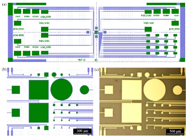
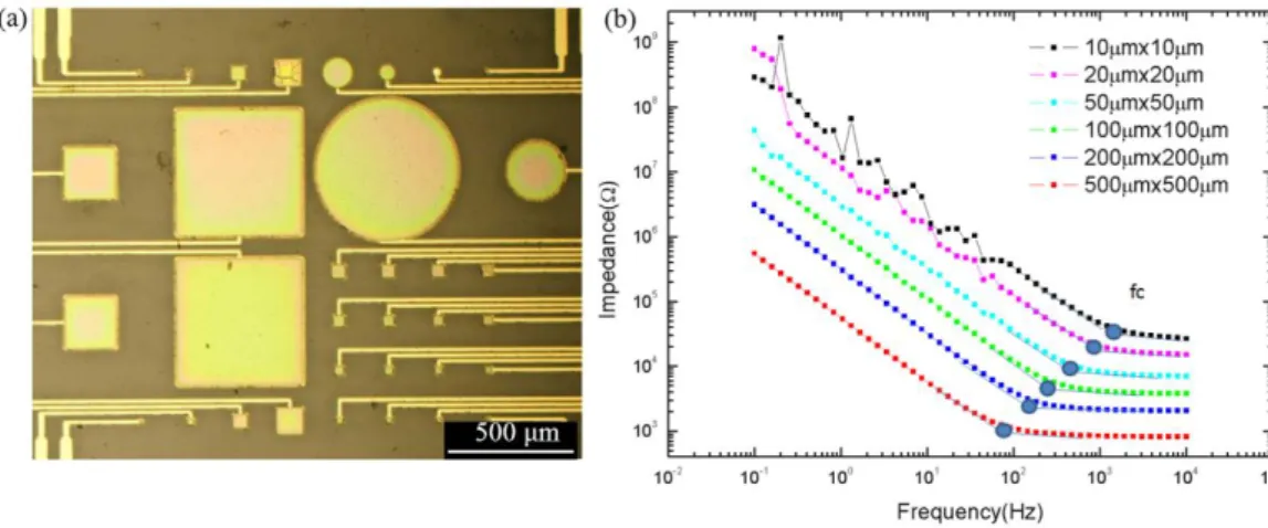
Figure 1.8: (a) The main steps of the fabrication process. The gold electrodes were first patterned lithographically and then Parylene-C was used for the device insulation. A second photolithography step followed by an etching step defines the well for the PEDOT:PSS deposition that follows. A mechanical peel off concludes the fabrication. (b) A Micro Electrode Array device fabricated on a glass slide (c) a close up of the PEDOT:PSS covered electrodes (scale bar 50 μm).[Reproduced with permission from Ref.3]
Once again, the method is generic and versatile, and it can be adapted regarding the desired device geometry. Moreover, different conducting polymers can be used as active layers as long as they can be deposited from solution.
Orthogonal photoresist method
A different way of dealing with the polymer patterning challenge comes with the utilization of orthogonal solvents. The term orthogonal refers to solvents in which the organic compounds are insoluble, a feature that allows not only the patterning of organic electronic materials but also their multilayer deposition.
Hydrofluoroethers (HFEs) , in particular belong to a class of solvents which, besides being nontoxic and environmental friendly, are also orthogonal to many organic materials[23]. Consequently, they are ideal candidates for polymer patterning as long as a photoresist compatible with them is synthesized.
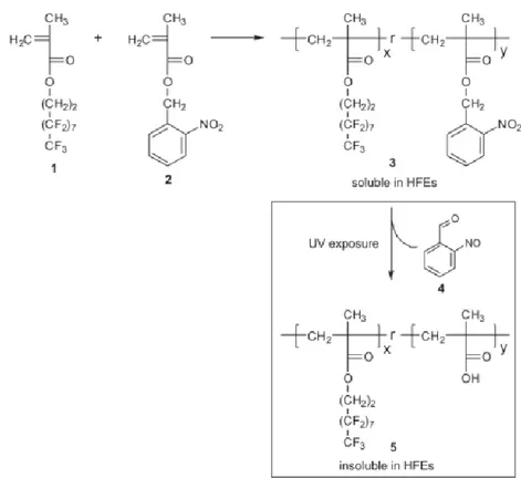
A photoresist like this was presented in 2009 by P.G. Taylor et al [10]. The HFE compatible material is a co-polymer composed of a highly fluorinated monomer 1 (3.3.4.4.5.5.6.6.7.7.8.8.9.9.10.10.10-Hepta-decafluorodecyl methacrylate) and a photosensitive monomer 2 (2-Nitro-benzyl methacrylate) (Fig 1.9). Its solubility can be modified after UV exposure from soluble to insoluble in HFEs solvents due to
25
structural changes to the photosensitive 2 part of the molecule, resulting in a negative tone photoresist. In addition, it is acid stable, a feature extremely useful when it is used to pattern acidic polymers.
Figure 1.9: Synthesis of the HFE-soluble photosensitive co-polymer 3. Exposure to UV light renders the polymer in soluble in HFEs. [Reproduced with permission from Reference 5]
As a proof of concept, a bottom contact organic thin field transistor was fabricated with a pentacene channel and PEDOT:PSS drain and source electrode by the same group. On a Si wafer, a 360 nm oxide was grown thermally just before PEDOT:PSS was spin cast and baked at 180oC for 10 min. Photoresist 3 was then spun on the PEDOT:PSS layer and patterned lithographically with HFE-7200 (an isomeric mixture of methyl nonafluorobutyl ether and methyl nonafluoroisobytl ether) acting as its developer. The image was transferred on the PEDOT:PSS with oxygen etching and the remaining photoresist was lifted off in a propan-2-ol (10% by volume)/HFE-7100 mixture. Photoresist 3 was spun again on the patterned PEDOT:PSS film, this time followed by UV light exposure and a development step. Pentacene was thermally evaporated and the photoresist removal in the previously used solvents mixture ended up a pentacene channel connecting the PEDOT:PSS source and drain electrodes(Figure 1.10).
26
Figure 1.10. Main fabrication steps of the PEDOT:PSS/Pentacene bottom-contact Organic Thin Film Transistor. PEDOT:PSS was first spin cast on the substrate and patterned photolithographically with the use of the photoresist 3 as a developer and a following oxygen etching step. The process was repeated for the deposition of the pentacene film giving birth to the organic thin film transistor. [Reproduced with permission from Reference .5] In a similar approach, H.S. Hwang and co-workers were able to pattern polymer materials using supercritical carbon dioxide (scCO2) as solvent[24] to
fabricate an OLED. ScCO2 is an environmental friendly fluid used in dry
photolithography process (DPP) for resist stripping due to its physical and chemical advantages. Most importantly, it is a poor solvent for most ionic, high molecular weight and low pressure organic materials.
In their work, a light emitting polymer (LEP) was patterned on top of a PEDOT:PSS active layer. PEDOT:PSS was first spin cast on glass coated with indium tin oxide (ITO). A negative tone co-polymer was synthesized from 1H,1H,2H,2H-perfluorodecyl methacrylate (FDMA) and tert-butyl methacrylate (TBMA) and deposited on the PEDOT:PSS layer. After UV exposure, scCO2 was used for the
development followed by oxygen plasma cleaning treatment and a LEP spin casting step. A thermally deposited CsF(1nm)/Al(40nm) film completed the ITO/PEDOT:PSS(CH8000) /LEP/CsF/Al structure (Figure 1.11).
Figure 1.11: The main steps of the OLED fabrication process. PEDOT:PSS was spun on the substrate and a negative tone photoresist was used to pattern the LEP on top of PEDOT:PSS. The developer used was sCO2 which is
not harmful to the active material. A CsF(1nm)/Al(40nm) film completes the device fabrication. [Reproduced with permission from Reference 20]
27
1.3 Concepts of Neuroscience
Brain is, without any doubt, the most marvelous and remarkable organ in the human body. It is the center where the stream of environmental signals is sorted out to those events that are important for the survival or the well-being of the individual. Putting in a different way, it is the center where perception is organized and either is stored in the memory for future reference or is translated into an immediate action[25].
Going a step further, brain is something more than just the center for moving and sensing functionality. It is the part of the body where processes like thinking and emotion creation take place, giving birth to the notion of consciousness. This is why Scientific American in 2014 named the new century the century of the brain. This is also why the new trend in science dictates large scales initiatives to facilitate recording and controlling brain activity as part of a greater effort to understand this extraordinary biological machine (e.g. “Human Brain Project”, “Brain Activity Map”). After all, the study of the brain is in its base the study of our own selves and mankind has always been fascinated by the idea knowing its inner world.
In practice, brain functionality is based on a very big number of interconnected nerve cells that form a complex information processing network. There are two main nerve cell classes participating in this task. The neural cells (or neurons) and the glia cells (or glia) [25, 26]. (Some scientists will argue there are three if we count the blood vessels as well. Blood vessels’ main role is to provide the neural cells with glucose, the basic energy fuel)
1.3.1 Neurons
Neurons are the basic units of the brain. Inside the human brain we can find a little bit less than 100 billion individual neurons a number of the same order of magnitude with the number of stars in the Milky Way Galaxy. These neurons can be further classified to a thousand different types. Nevertheless, it is more the organization of them into different neuronal circuits that creates the complexity of the human behavior and less their variety. In other words, the same type of neurons can participate in different signaling function depending the way they are interconnected with other neural cells.
28 1. The cell body (or soma)
2. The dendrites 3. The axon
4. The presynaptic terminals
Figure 1.12 :Schematic of a typical neural cell[27].
The cell body is the metabolic center of the cell and the part of the cell where the nucleus is located. As a consequence, this is where the protein synthesis takes place. There are two kinds of processes that arise out of the soma. The fine branching structure of many short dendrites and a single long axon. Dendrites’ role is to receive information from other cells while the axon’s to send signals to other cells. These signals are of electrical nature and propagate in the form of Action Potentials (AP). The term action potential refers to a fast membrane depolarization event (initially the inside of neuron membrane is negative in respect to the positive extracellular area) and a subsequent re- polarization. Nevertheless, neurons are not only electrical active
29
cells they are also secretory ones. They secret molecules through their presynaptic terminals, the fourth of their distinct part. These molecules are called neurotransmitters and are the chemical substances that alters the electrical properties of the target cell by binding to special transmembrane proteins called neurotransmitter receptors [25, 26]. The overall idea is that neurons transform the signal that they receive as a molecular input into an electrical one that can travel faster to the next neuron where it can be changed back to its chemical form before interacting with it.
Neuron can be classified into three major categories regarding their form. Thus we can talk about 1) Unipolar 2) Bipolar and 3) Multipolar neurons
Figure 1.13 : Neural cell classification [27].
This classification is based on the number of processes emerging from the cell body but it has significance in the neuron’s functionality as well. For example unipolar neurons are mainly found in the invertebrate nervous system and in the autonomic nervous system of the vertebrate animals. They have only one process which is later divided into an axon and a dendrite brunch. Bipolar on the other hand,
30
are mainly sensory neurons with their dendritic part able to receive information from the periphery of the body while their axonal part forwards this information to the brain. A special subcategory of bipolar cells is the pseudo-unipolar which are the cells that transfer information of pain, pressure and touch to the spinal cord (DRG cells). Last but not least, multipolar neurons are the ones that we can find in abundance in the neuron system of the vertebrate kingdom .They have one axon and many dendrites which allows them to make a number of different connections with other neurons[25].
1.3.2 Glia
The term glia (γλία) comes from the Greek language and it means glue. It was conceived in 1895 by Rudolf Virchof as an effort to describe an “inactive substance” that holds the nerves together in the central nervous system [28]. Yet, glia does not really hold the neurons together. Instead, it surrounds them having a supporting to them role.
Glia cells are morphologically very different from the neurons as they do not have the typical soma-axon-dendrite structure of the later. In general, they present a remarkable diversity linked to their multi functionality and outnumber neurons by a factor of 2 to 10. Nevertheless, glia on vertebrates can by divided in two major categories. Microglia and Macroglia[25].
Microglia are cells of the immune system while Macroglia has a slightly different more supporting role and is subdivided into Oligodentrocytes, Schwan cells and Astrocytes. For the first two (Oligodentrocytes and Schwan cells) there is not much of a dispute regarding their role. We know, today, that these are the cells that provide an insulating layer, called myelin, which is essential for the fast transfer of the electrical signals between the neurons.
Nevertheless, Astrocytes’ role is still a mystery for the scientific community. We believe that their main function is to retain the central nervous system homeostasis[28]. It is believed that they do not take part in information processing but they provide neural support in four ways [25] :
1) They separate cells and thus provide electrical insulation between neuronal groups.
![Figure 1.1: The two way coupling between organic electronic devices and biology [1] . For the reasons above, organic electronics seems to be the ideal candidate for allowing bioelectronics to fulfil its true potential](https://thumb-eu.123doks.com/thumbv2/123doknet/11504773.293805/13.892.230.715.122.390/figure-coupling-electronic-electronics-candidate-allowing-bioelectronics-potential.webp)
![Figure 1.15: Plot of the phases of an action potential [30] .](https://thumb-eu.123doks.com/thumbv2/123doknet/11504773.293805/40.892.263.682.106.382/figure-plot-phases-action-potential.webp)