Contact region fidelity, sensitivity, and control in
roll-based soft lithography
by
ARCHNES
IMASSACHUSET- INS rE
Joseph Edward Petrzelka
OFTECHNOLOGYB.S., Iowa State University (2007)
JUN 28201
M.S., Iowa State University (2009)
LIBRARIES
Submitted to the Department of Mechanical Engineering
in partial fulfillment of the requirements for the degree of
Doctor of Philosophy
at the
MASSACHUSETTS INSTITUTE OF TECHNOLOGY
June 2012
©
Massachusetts Institute of Technology 2012. All rights reserved.
A uthor ...
...
.
...
Depar ment of Mechanical Engineering
May 11, 2012
C ertified by ...
...
David E. Hardt
Ralph E. and Eloise F. Cross Professor of Mechanical Engineering
Thesis Supervisor
Accepted by
....
....
...
David E. Hardt
Chairman, Department Committee for Graduate Students
Contact region fidelity, sensitivity, and control in roll-based
soft lithography
by
Joseph Edward Petrzelka
Submitted to the Department of Mechanical Engineering
on May 11, 2012, in partial fulfillment of the
requirements for the degree of Doctor of Philosophy
Abstract
Soft lithography is a printing process that uses small features on an elastomeric stamp to transfer micron and sub-micron patterns to a substrate. Translating this lab scale process to a roll-based manufacturing platform allows precise control of the stamp contact region and the potential for large area, high rate surface patterning. In this manner, emerging devices can be produced economically, including flexible displays, distributed sensor networks, transparent conductors, and bio-inspired surfaces.
Achieving and maintaining collapse-free contact of the soft stamp features is a necessary condition for printing. In the first part of the thesis, stamp behavior is examined at two length scales. First, microfeature collapse is examined across a range of dimensionless aspect ratios and pattern ratios to determine the collapse mode and the feature stiffness. Second, behavior of roll-mounted stamps is investigated on the macroscopic scale.
The results of these analyses, simulations, and experiments show that contact is prohibitively sensitive as the feature scale shrinks to single microns or below. In the second part of the thesis, methods are developed to reduce the contact sensitivity. A compliant stamp architecture is introduced to tune the mechanical response of the stamp. Next, a new process for manufacturing cylindrical stamps is developed that removes limitations of planar stamp templates.
The third part of the thesis addresses process control. A parallel kinematic stage is designed to manipulate the height and pitch of a roll over a substrate with submicron precision. A hybrid state-space
/
classical feedback control approach is used to achieve high bandwidth servo control in the presence of coupling and unmodeled dynamics. Using optical instrumentation, the stamp contact pattern is monitored and can be controlled using camera images as a control variable. Ultimately, a practical method of impedance control is implemented that demonstrates excellent disturbance rejection. The results of this thesis provide models for stamp behavior at the local microscale and the roll-based macroscale. These results illustrate the high sensitivity of contact to displacement disturbances in roll-based lithography, but also provide valuable de-sign insight towards dede-signing stamps and processing machinery that are robust tothese inherent disturbances.
Thesis Supervisor: David E. Hardt
Acknowledgements
This thesis, or even studying at MIT, would never have been possible without the support of innumerable individuals. My trajectory has been altered in some way by almost every faculty member, project team, or support staff that I've encountered. I am sincerely grateful to everyone who has taken the time to teach, critique, mentor, or just listen. Several people have been overwhelmingly instrumental in my success, and warrant individual mention here:
Prof. David Hardt is arguably the best advisor I've ever encountered. His men-toring, guidance, latitude in research direction, and positive attitude have made my time at MIT a distinct pleasure. The committee members - Prof. Martin Culpepper and Dr. Brian Anthony - provided excellent insight and advice.
My transition to the mechanical engineering program at MIT would not have been possible without the support my peers. The LMP student community, especially Matt Dirckx, Melinda Hale, Bob Panas, and Maria Telleria. Surviving qualifiers and producing a thesis would not have been possible without countless consults, cubicle conversations, and lunches. My sanity would not be intact without Wil Selby and Ashley Browning, who reminded me to live life outside of 77 Massachusetts Avenue. Finally, though perhaps most importantly, my wife, Jenna, has been incredibly supportive both during my MS and Iowa State and my PhD at MIT. Her belief in my goals and aspirations has propelled me well beyond what I might have ever achieved on my own.
Contents
I
Introduction
31
1 Introduction 33 1.1 Thesis Contributions . . . . 33 1.2 Lithographic Techniques . . . . 35 1.2.1 Conventional Lithography . . . . 35 1.2.2 Photolithography . . . . 36 1.2.3 Hybrid Lithography . . . . 37 1.3 M icrocontact Printing . . . . 38 1.3.1 M onolayer Inks . . . . 39 1.3.2 Stamp Replication . . . . 40 1.3.3 M aterial Systems . . . . 41 1.3.4 Outlook . . . . 43 1.4 Printing Applications . . . . 44 1.4.1 Active Surfaces . . . . 44 1.4.2 Passive Surfaces . . . . 45 1.5 M anufacturing Challenges . . . . 46 1.5.1 Feature Deformation . . . . 46 1.5.2 Accuracy . . . . 47 1.5.3 M achine Implementations . . . . 481.5.4 Roll Based Processing . . . . 49
1.5.5 Grand Challenge . . . . 50
II Contact Behavior
2 Polymer Mechanics
2.1 PDMS Composition . . . . 2.2 Material Deformation . . . . 2.3 Constitutive Models . . . . 2.3.1 Small Deformation Elasticity 2.3.2 Finite Deformation Elasticity 2.3.3 Stiffening Finite Deformation 2.3.4 Incompressibility . . . . 2.4 Material Characterization . . . . .
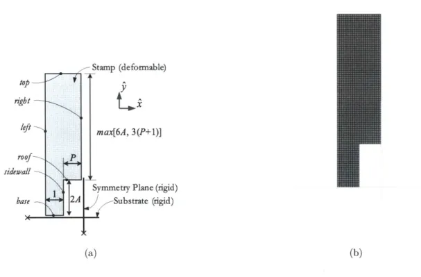
3 Stamp Feature Deformation 3.1 Feature Collapse . . . . 3.2 Analytical Models . . . . 3.2.1 Notation . . . . 3.2.2 Stiffness . . . . 3.2.3 Collapse Onset . . . . 3.2.4 Summary . . . . 3.3 Numerical Simulation . . . . . 3.3.1 Geometry . . . . 3.3.2 Meshing . . . . 3.3.3 Material Model . . . . 3.3.4 Boundary Conditions . 3.3.5 Loading . . . . 3.3.6 Implementation . . . . 3.3.7 Interpreting Results . . 3.4 Experimental Methods . . . . 3.4.1 Experiment Design . . 3.4.2 Test Specimens . . . . 3.4.3 Experimental Protocol
53
55 55 56 58 58 58 59 60 61 Elasticity 65 . . . . 6 5 . . . . 6 7 . . . . 6 7 . . . . 6 9 . . . . 7 2 . . . . 7 9 . . . . 7 9 . . . . 7 9 . . . . 8 0 . . . . 8 1 . . . . 8 1 . . . . 8 2 . . . . 8 2 . . . . 8 4 . . . . 8 6 . . . . 8 6 . . . . 8 7 . . . . 8 83.4.4 Data Collection . . . .. . . . 92 3.4.5 M aterial Characterization . . . . 92 3.4.6 M easurement Repeatability . . . . 93 3.5 Results . . . . 93 3.5.1 Stiffness . . . . 93 3.5.2 Roof Collapse . . . . 99 3.5.3 Buckling . . . . 101
3.5.4 Failure M ode Prediction . . . . 103
3.6 Discussion . . . . 106
3.6.1 Experimental Agreement . . . . 106
3.6.2 Scaling . . . . 106
3.6.3 Alternative Geometry . . . . 107
3.7 Summary . . . . 108
4 Roll Based Contact Mechanics 111 4.1 Roll Based Stamp Contact . . . . 111
4.2 Contact M echanics . . . . 114 4.2.1 Curvature M apping . . . . 115 4.2.2 Hertz Contact . . . . 116 4.2.3 Elastic Layer . . . . 117 4.2.4 Elastic Foundation . . . . 118 4.2.5 W ork of Adhesion . . . . 118
4.3 Feature Continuum Viewpoint . . . . 121
4.4 Analytical M odels . . . . 123 4.4.1 Small Features . . . . 123 4.4.2 Compliant Features . . . . 128 4.4.3 Surface Energy . . . . 130 4.5 Numerical Simulation . . . . 130 4.5.1 Geometry . . . . 130 4.5.2 M eshing . . . . 131
4.5.3 Material Model . . . 4.5.4 Boundary Conditions . . . . 132 . . . . 133 4.5.5 Loading . . . . 4.5.6 Implementation . . . . 4.5.7 Interpreting Results . . . . 4.6 Experimental Methods . . . . 4.6.1 Experiment Design . . . . 4.6.2 Test Specimens . . . . 4.6.3 Experimental Apparatus . . . 4.6.4 Data Collection . . . . 4.6.5 Material Characterization 4.6.6 Experiment Accuracy ... 4.7 Results . . . . 4.7.1 Elastic Layer Simulation . . . 4.7.2 Elastic Foundation Simulation 4.7.3 Work of Adhesion . . . . 4.7.4 Experimental Data . . . . 4.8 Discussion and Summary . . . .
III Robust Stamp Design
5 Stamp Architecture 5.1 Process Sensitivity . . . . 5.1.1 Error Sources . . . . 5.1.2 Process Window . . . . 5.1.3 Spatial Frequency . . . . 5.2 Robust Stamp Design . . . . 5.2.1 Feature Design. . . . . 5.2.2 Stamp Design . . . . 5.2.3 Compliant Architecture . . . . . . . . 133 . . . . 136 . . . . . 136 . . . . . 137 . . . . . 137 . . . . . 139 . . . . . 140 . . . . . 142 . . . . . 143 . . . . . 143 . . . . . 144 . . . . . 144 . . . . . 147 . . . . . 149 . . . . . 151 157159
161 . . . . 161 . . . . 162 . . . . 164 . . . . 164 . . . . 167 . . . . 167 . . . . 170 . . . . 1745.3 Contact Analysis . . . . 177
5.3.1 Euler Beam Theory . . . . 178
5.3.2 Timoshenko Beam Theory . . . . 180
5.3.3 Elastic Layer . . . . 181 5.3.4 Numerical Solution . . . . 183 5.4 Results . . . . 186 5.4.1 Numerical Data . . . . 186 5.4.2 Experimental Data . . . . 189 5.4.3 Discussion . . . . 192 5.5 Case Study . . . . 192 5.6 Summary . . . . 195 6 Stamp Casting 197 6.1 Stamp Replication . . . . 197 6.1.1 M aster Templates . . . . 197
6.1.2 Conventional Stamp Casting . . . . 199
6.1.3 Conventional Stamp M ounting . . . . 200
6.1.4 Challenges . . . . 200 6.2 Cylindrical Stamps . . . . 202 6.3 Centrifugal Coating . . . . 205 6.3.1 Fluid Dynamics . . . . 205 6.3.2 Photoresist . . . . 212 6.3.3 PDM S . . . . 214 6.4 M achine Design . . . . 215 6.4.1 Centrifuge . . . . 215
6.4.2 Direct W rite Optics . . . . 217
6.4.3 System Integration . . . . 223
6.4.4 Servo Control . . . . 225
6.5 Experim ent . . . . 229
6.5.2 Measurement and Results . . . . 6.6 Sum m ary . . . .
IV
Process Control
7 Machine Design 7.1 Motivation . . . . 7.2 Design . . . . 7.2.1 Design Concept . 7.2.2 Bearings . . . . 7.2.3 Actuators . . . . 7.2.4 Sensors . . . . 7.2.5 Mounting . . . . 7.2.6 System Model . . . . . 7.3 Characterization . . . . 7.3.1 Sensors . . . . 7.3.2 Flexural Bearings and 7.3.3 Linearity . . . . 7.3.4 Repeatability . . . . . 7.3.5 Shaft Runout . . . . . 7.3.6 Structural Loop . . 7.3.7 Dynamic Response 7.4 Summary . . . . 8 Machine Control8.1 Parallel Kinematic Dynamics 8.2 Nested Control Architecture
8.2.1 Controller Synthesis 8.2.2 Unmodeled Dynamics 8.3 Position Control . . . . 8.3.1 Loop Shaping... 245 . . . . 245 Actuators . . . . 247 . . . . 247 . . . . 248 . . . . 251 . . . . 254 . . . . 256 . . . 259 . . . 262 . . . 262 . . . 267 . . . . 267 . . . . 268 . . . . 271 . . . . 271 . . . . 271 . . . . 274 275 . . . . 275 . . . . 276 . . . . 278 . . . 279 . . . 281 . . . 284 234 241
243
8.4 Summary ... . 8
9 Process Feedback Control 287 9.1 Process Control ... ... 287
9.2 Contact Imaging . . . . 288
9.2.1 Total Internal Reflection . . . . 288
9.2.2 Perspective Correction . . . . 292
9.3 Contact Measurement . . . . 296
9.3.1 Thresholding . . . . 296
9.3.2 Edge Finding . . . . 299
9.3.3 Robustness . . . . 302
9.4 Contact Feedback Control . . . . 303
9.4.1 Plant model . . . . 304 9.4.2 Controller design . . . . 305 9.4.3 Experimental Results. . . . . 307 9.5 Impedance Control . . . . 309 9.5.1 Controller Design . . . . 309 9.5.2 Experimental Results. . . . . 311
9.6 Summary and Outlook . . . . 316
V
Conclusion
319
10 Conclusion 321 10.1 Contributions . . . . 32110.1.1 Stamp Deformation . . . . 321
10.1.2 Stamp Design and Manufacture . . . . 322
10.1.3 Process Control . . . . 324 10.2 Design Example . . . . 324 10.2.1 Design Approach . . . . 325 10.2.2 Grating Example . . . . 326 10.2.3 TFT Interconnect Example . . . . 331 286
10.3 Extensions . . . . 336 10.4 Future Challenges . . . . 337 10.5 Outlook . . . . 339
List of Figures
1-1 Microcontact printing process . . . . 1-2 Self assembling monolayers as etch resists . . . .
1-3 Effect of mechanical stamp deformation on pattern trasnfer . 1-4 Stamp application modes . . . .
2-1 PDMS monomer . . . .
2-2 Tensile testing specimen . . . . 2-3 Fitting modulus to tensile test data . . . .
3-1 3-2 3-3 3-4 3-5 3-6 3-7 3-8 3-9 3-10 3-11 3-12 3-13 3-14 3-15
Microfeature collapse modes . . . . Stamp geometry and feature dimensions . . . . . Stamp feature analytical limits . . . .
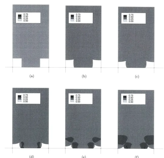
Feature buckling load paths . . . . Schematic of feature lateral collapse . . . . Micrographs of lateral feature collapse. . . . . Feature numerical simulation geometry . . . . Feature numerical simulation frames . . . .
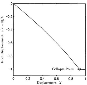
Feature stiffness in numerical simulations . . . . . Roof collapse in numerical simulations . . . .
Experimental construct and contact visualization Feature loading experimental apparatus . . . . Experimental feature collapse images . . . . Analytic v. numeric feature stiffness . . . . Analytic series model v. numeric feature stiffness
38 39 . . . . . 47 49 56 62 63 . . . . 65 . . . . 68 . . . . 70 . . . . 75
. . . .
77
. . . . 78 . . . . 80 . . . . 83 . . . . 85 . . . . 86 . . . . 88 . . . . 89 . . . . 91 . . . . 94 . . . . 953-16 3-17 3-18 3-19 3-20 3-21 3-22 3-23 3-24 3-25 4-1 4-2 4-3 4-4 4-5 4-6 4-7 4-8 4-9 4-10 4-11 4-12 4-13 4-14 4-15 4-16 4-17 4-18 4-19
Closed form v. numeric feature stiffness . . . . Correction of experimental data with control data Maximum experimental feature displacement . . . Experimental feature stiffness . . . . Experimental roof collapse pressure . . . . Experimental feature roof collapse displacement . Typical experimental feature buckling curve . . . Experimental feature buckling load . . . . Experimental feature collapse modes . . . . Collapse mode boundaries as a function of scale . Stamp feature deformation modes . . . . Roll-mounted stamp contact problem . . . .
Stamp dimensions and loading parameters . . . .
Limits of stamp architecture . . . . Load path accounting for surface energy . . . . . Stamp elastic bilary model . . . . Elastic layer material deformation . . . .
Stamp numeric simulation implementation . . . .
Typical roll-based stamp simulation results . . . .
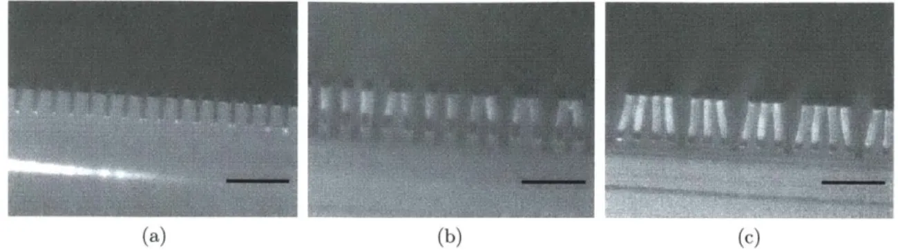
Typical contact simulation results as a function of Stamp casting mold . . . . Stamp replication from master . . . . Experimental stamp loading apparatus . . . . Experimental load profile . . . . Experimental stamp contact images . . . . Experimental roll based load-displacement curves
Numerical v. analytical elastic layer model . . . .
Numerical v. analytical elastic foundation model . Effect of surface energy on numerical model . . .
. . . . 96 . . . . 97 . . . . 98 . . . . 99 . . . . 100 . . . . 101 . . . . 102 . . . . 103 . . . . 105
. . . 107
. . . . 111 . . . . 113 . . . . 113 . . . . 114 . . . . 120 . . . . 121 . . . . 124 . . . . 132 . . . . 135 surface energy . . 137 . . . . 139 . . . . 140 . . . . 141 . . . . 141 . . . . 142 . . . . 144 . . . . 146 . . . . 148 . . . . 1504-20 Hysteresis in roll contact experiments . . . . 151
4-21 Experimental elastic layer results . . . . 154
4-22 Experimental elastic foundation results . . . . 155
4-23 Experimental elastic foundation results . . . . 156
5-1 Fishbone diagram of disturbance sources . . . . 162
5-2 Spatial frequency of process disturbances . . . . 165
5-3 Feature collapse pressure and displacement for robust feature design . 169 5-4 Backing layer architecture . . . . 175
5-5 Backing layer architecture . . . . 176
5-6 Beam theory analogy of backing layer behavior . . . . 177
5-7 Calculated contact behavior for backing layer beam theory models . . 185
5-8 Numerical simulation of backing layer . . . . 187
5-9 Backing layer analytical model v. numerical simulations . . . . 188
5-10 Experimental backing layer results . . . . 190
5-11 Experimental backing layer results . . . . 191
5-12 Hexagonal pattern used in backing layer case study . . . . 193
5-13 Test pattern experimental load behavior . . . . 194
6-1 Coating steps in cylindrical stamp casting . . . . 203
6-2 PDMS stamp made with the proposed centrifuge process . . . . 204
6-3 Characteristic dimensions of a rimming flow in a horizontal centrifuge 206 6-4 Rectilinear approximation of thin fluid layer in a centrifuge . . . . 207
6-5 Sensitivity of centrifuge drum to leveling error . . . . 212
6-6 Kinematic viscosity of SU8 photoresist versus solvent fraction . . . . 213
6-7 Centrifuge bearing design . . . . 216
6-8 Assembled centrifuge . . . . 217
6-9 Guassian beam irradiance profile . . . . 218
6-10 Gaussian beam waist . . . . 219
6-11 Single element optics focusing . . . . 220
6-13 6-14 6-15 6-16 6-17 6-18 6-19 6-20 6-21 6-22 6-23 6-24 6-25 6-26 6-27 6-28 7-1 7-2 7-3 7-4 7-5 7-6
7-7
7-8 7-9 7-10 7-11 7-12Laser optics design using C-mount components . . . . . Assembled focusing optics . . . . Schematic of direct write machine . . . . Complete direct-write system . . . .
Centrifuge controller block diagram. . . . . Optical stage controller block diagram. . . . . Curing the planarizing layer of photoresist . . . . Transmittance of SU8 . . . . Method of mounting cylindrical stamps to rolls . . . .
Patterned centrifuge drum and corresponding stamp . . Laser exposure level experiment . . . . Surface roughness of planarizing layer . . . . Core samples for stamp thickness measurement... Interferometer data showing core sample height . . . .
Stamp thickness uniformity . . . .
Micrographs of direct-write features replicated in PDMS
Simply supported shaft concept . . . . Shaft end bearing degrees of freedom . . . . Parallel flexure design . . . .
Flexure dynamic modes . . . .
Actuator and sensor placement on flexural bearings . . Strain gage configuration on flexures . . . .
Schematic of shaft and bearing assembly . . . . Precision roll positioning stage . . . . M achine kinematics . . . . Position sensor calibration . . . . Velocity sensor calibration . . . . Time domain position sensor noise . . . .
7-13 Spectral density of position sensor noise . . . 266
. . . . 222 . . . . 223 . . . . 224 . . . 225 . . . 226 . . . . 228 . . . . 231 . . . . 232 . . . . 233 . . . . 234 . . . . 235 . . . . 236 . . . . 237 . . . . 238 . . . 239 stamps . . . 240 . . . . 246 . . . . 248 . . . . 249 . . . . 252 . . . . 253 . . . 254 . . . 257 . . . 258 . . . 259 . . . 263 . . . . 264 . . . . 265
Time domain of repeatability error . .
Spectral density of repeatability error . Open loop frequency response . . . . .
Nested feedback loop architecture . . .
Block diagram of an R2 MIMO system Frequency response of shaped plant Loop shaping compensator design .
Time domain step response . . . .
7-14 7-15 7-16 8-1 8-2 8-3 8-4 8-5 9-1 9-2 9-3 9-4 9-5 9-6 9-7 9-8 9-9 9-10 9-11 9-12 9-13 9-14 9-15 9-16 9-17 10-1 10-2 10-3 269 270 273 278 280 283 285 286 . . . . 289 . . . . 291 . . . . 292 . . . . 293 . . . . 295 . . . . 298 . . . . 301 . . . . 302 . . . . 303 . . . . 304 . . . . 308 . . . . 310 . . . . 311 . . . . 313 . . . . 314 . . . . 315 . . . . 316
TIR contact imaging technique . . . .
Perspective distortion of contact interface image . . .
Optics mounting in the roll positioning stage . . . . . Image correction perspective mapping . . . . Example of camera image calibration . . . . Thresholding method of contact measurement . . . .
Example of contact measurement using edge finding Example of contact measurement by edge finding .
Robustness of contact measurement . . . . Block diagram of contact feedback control . . . . Contact feedback control results . . . . Impedance control block diagram . . . . Roll impedance measurement . . . .
Impedance control results . . . . Impedance control disturbance rejection experiment . Impedance control disturbance rejection results . . .
Impedance control repeatability . . . .
Grating pattern example: design of printing features Grating pattern example: design of backing features Grating pattern example: selection of roll preload .
327 328 330
10-4 TFT pattern example: design of printing features . . . . 332 10-5 TFT pattern example: design of backing features . . . . 333 10-6 TFT pattern example: selection of roll preload . . . . 335
List of Tables
1.1 A survey of stamp defect modes reported in literature . . . . 46
3.1 Boundary condition constants for Euler column buckling . . . . 74
3.2 Feature numeric simulation parameters . . . . 79
3.3 Microfeature simulation boundary conditions . . . . 81
3.4 Microfeature simulation contact conditions . . . . 82
3.5 M ask D esign . . . . 87
3.6 Feature experimental parameters . . . . 88
3.7 Feature measurement repeatability . . . . 93
4.1 Roll-based stamp simulation boundary conditions . . . . 133
4.2 Roll-based stamp simulation contact conditions . . . . 133
4.3 Stamp topologies and material parameters in roll contact experiments 138 5.1 Experimental parameters for stamps with backing layers . . . . 186
5.2 Case study stamp parameters . . . . 193
5.3 Predicted collapse displacement of case study pattern . . . . 194
6.1 DC brush motor characteristics . . . . 216
6.2 Direct write laser specifications . . . . 220
6.3 Stamp thickness analysis of variance . . . . 238
7.1 Actuator specifications . . . . 253
7.2 Calibrated sensor gains . . . . 263
7.4 System model parameters . . . . 272
9.1 Index of refraction for optical materials . . . . 290 9.2 Camera perspective calibration constants from calibration . . . . 294
10.1 Grating pattern stamp design example . . . . 329
10.2 TFT interconnect stamp design example . . . . 334
Nomenclature
a
Image foreshortening correction factor, page 293 as Timoshenko beam theory shear factor, page 180Image perspective correction factor, page 293
3 Volume fraction of solids in photoresist solution, page 214
C: Error vector used to assess roll positioning stage repeatability, page 268
E Material infinitesimal deformation gradient tensor, page 57
a- Material stress tensor, page 58
b Fluid body force, page 206
E Material strain tensor, page 57
F Material deformation gradient tensor, page 56
G(s) Frequency domain transfer function matrix, page 279 H Material displacement gradient tensor, page 56
K State feedback matrix, page 277
u Actuator effort vector in roll positioning stage dynamic equation, page 262
u Material displacement vector, page 56
x Dynamic state vector in roll positioning stage dynamic equation, page 262
y Output vector in roll positioning stage dynamic equation, page 262
ur Reference roll contact force superimposed on roll during impedance control,
page 310
6 Roll displacement towards substrate, page 112
* Local effective roll displacement, page 164
o Equilibrium roll displacement (neglecting surface energy), page 119 6
eq Equilibrium roll displacement (considering surface energy), page 119
6
flexure Displacement of a flexural bearing comprised of individual flexure blades,
page 250
C Dimensional errors along
Q
at the stamp contact interface, page 162E Surface strain at the root of a flexure blade, page 250
YS Material surface energy, page 67
Nominal or mean roll displacement, page 164
K Material bulk modulus, page 58
Ko Initial material bulk modulus (finite deformation elasticity), page 59
A Material stretch, page 58
A Wavelength of light, page 219
Aepsilon Roll displacement error wavelength, page 165 Af Fluid asperity wavelength in a centrifuge, page 211
Am Maximum locking stretch, Arruda-Boyce model, page 59
C2 Criterion for applicability of elastic foundation model, page 129
C3 Criterion for applicability of elastic foundation model in backing layer stamps,
page 183
DC(s) Decoupling criterion, page 279
P Fluid dynamic viscosity, page 206
P Material shear modulus, page 58
Po Initial material shear modulus (finite deformation elasticity), page 59
v/ Fluid kinematic viscosity, page 206
v Material Poisson ratio, page 61
W Centrifuge velocity in the b direction, page 206
p Beam radius of curvature, page 172
p Fluid density, page 206
Pm Material radius of curvature, page 173
o Fluid surface tension, page 199
oo Stamp microfeature far-field pressure, page 68
oy Yield stress, page 250
r Net actuator torque on roll in the 0 direction, page 260
Tf Fluid asperity decay time constant in a centrifuge, page 211
E
Gaussian beam waist divergence angle, page 2190 Incident angle of a light ray relative to a surface normal vector, page 289
A Stamp microfeature aspect ratio, dimensionless, page 68
a Stamp microfeature spacing, page 67
b Thickness of flexure blade, page 249
bc Buckling boundary condition, page 74
bi Damping of each flexural bearing,
i
= 1, 2, page 261Ci(s) Frequency domain compensators in a RV system, i = I...n, page 278
C10 Neo-Hookean material parameter, page 59
Cf Conformability, dimensionless ratio of surface energy and strain energy, page 69
D Collimated Gaussian beam diameter, page 220
Di Neo-Hookean material parameter, page 59
E Material elastic modulus, page 61
E* Plane strain elastic modulus, page 70
EO Initial material elastic modulus (finite deformation elasticity), page 61
E, Roll displacement error in the spatial frequency domain, page 165
f
Contact force between roll and substrate per unit length of roll, page 112f
Focal length, page 220f
Net actuator force on roll in the i direction, page 260fi
Force of an actuator, i = 1, 2, page 250g Gravitational field magnitude, page 206
GF Strain gage 'gage factor', page 255
h Height of flexure blade, page 249
h Stamp microfeature height, page 67
I
Beam moment of inertia, page 74I Camera image in the form of an array of discrete pixels, page 299
I Gaussian beam irradiance, page 218
I* Aggregate vector of image array I, page 300
Io
Gaussian beam irradiance at the beam axis, page 218I1 First invariant of material deformation, page 59
J
Material volume ratio, page 57J
Sprung rotational inertia of shaft and flexural bearings, page 261K Stamp microfeature stiffness, dimensionless, page 69
k Stamp microfeature sheet stiffness, page 69
k* Equivalent microfeature stiffness in stamps with backing features, page 181
kb Sheet stiffness of stamp backing features, page 175
K, Stamp microfeature stiffness (limit of small aspect ratio), page 71
ki Stiffness of each flexural bearing, i = 1, 2, page 261
kP Sheet stiffness of stamp printing features, page 175
kbeam Stiffness of flexure blade from beam theory, page 249
kflexure Stiffness of a flexural bearing comprised of individual flexure blades, page 250
KII Stamp microfeature stiffness (limit of large aspect ratio), page 72
I Contact length between roll and substrate along the 1 direction, page 112
1 Length along roll axis 2 between flexural bearing pivots, page 259
1 Length of flexure blade, page 249
10 Equilibrium roll contact length, page 119 12 Centrifuge drum length, page 206
la Stamp length along roll axis 2, page 112
m Sprung mass of shaft and air bushings, page 261 n Optical index of refraction, page 289
n Plastic yield safety factor, page 250
P Gaussian beam power, page 219
P Stamp microfeature pattern ratio, dimensionless, page 68
p Fluid hydrostatic pressure field, page 206 p Hydrostatic pressure field, page 60
p(x) Contact pressure distribution between roll and substrate, page 112
Po Center (maximum) contact pressure between roll and substrate, page 112 pC Stamp microfeature collapse pressure, page 109
q Beam loading function, page 177 r Centrifuge drum radius, page 206 r Roll radius, page 112
r* Equivalent roll radius in a two-roll system, page 115
Sbuckle Stamp microfeature buckling pressure, page 76
S, Stamp microfeature collapse pressure, page 72
t Stamp thickness, page 67
U Strain energy, page 59
u Fluid velocity vector component in the J direction, page 207
u Material displacement component along 1, page 56
v Fluid velocity vector component in the
Q
direction, page 207v Material displacement component along
Q,
page 56vOC Stamp microfeature far-field displacement, page 68
Vb Strain gage bridge driving voltage, page 255 V Velocity sensor gain, i = 1, 2, page 256
w Beam neutral axis displacement, page 177
w Gaussian beam diameter, page 218
w Stamp microfeature width, page 67
wo Gaussian beam waist diameter, page 218
Wad Interface work of adhesion, page 67
W,*d Effective interface work of adhesion, page 75
X Stamp microfeature far-field displacement, dimensionless, page 69
y Roll height as a degree of freedom in positioning stage, along
Q,
page 246 y, Position of roll endpoints in a simply supported configuration, i 1, 2, page 246Part I
Chapter 1
Introduction
Contact lithography holds the potential to pattern large areas of micro- and nano-scale features at high rates by using mechanical contact to replicate patterns. In recent years, interest has risen in adapting contact lithography processes to roll based platforms to enable large area printing of micro- and nano-scale features, including mi-crocontact printing [87] and nanoimprint lithography [1]. Successful implementation of contact lithography in roll based platforms would enable scalable manufacturing of flexible engineered metasurfaces, electronics, displays, and sensor systems.
This thesis examines microcontact printing from the perspective of the elastomeric stamp contact interface. The three central parts of this thesis examine (i) fundamen-tal contact phenomena, (ii) stamp design and manufacture, and (iii) process control schemes. Ultimately, the thesis contributes a holistic understanding of stamp defor-mation behavior, a new stamp architecture and casting technique for robust printing, and a machine model for precision roll-based manufacturing.
1.1
Thesis Contributions
This thesis provides contributions to both (i) the theoretical understanding of elas-tomeric stamp behavior and (ii) ways that this behavior can be used to create robust printing through new machine and process designs.
collapse mode of microscale stamp features. The stiffness of individual stamp features is established as a function of feature geometry. Using this stiffness result, a unified theory is developed that maps feature collapse modes as a function of dimensionless geometrical, material, and load parameters. The experimental method developed is used to validate these models of stiffness and collapse mode. This result predicts the acceptable pressure or displacement imposed on any particular microfeature, which in turn guides robust stamp design and establishes an upper bound on feasible stamp contact stresses.
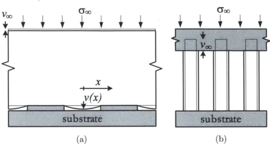
The contact pressure evolution in roll mounted stamps is derived by augmenting classical contact mechanics solutions in the limit of either very small or very compliant stamp features. The models developed are validated using numeric simulation and experimental studies on a custom designed lab scale rolling stage. The results of these models illustrate that the stamp contact behavior has a significant dependence on the microscale stamp features, even when the body of the stamp is many times thicker than the characteristic feature dimensions. Combining the prior bound on stamp contact stresses with these models provides feasible roll displacements or contact errors.
A feasible process window for roll based processing is developed using the roll based contact models. Design opportunities for a large (robust) process window are discussed and compared to reports in the literature. A new stamp architecture is developed to dramatically increase this process window beyond the ability of conven-tional stamp designs. Analytical, numerical, and experimental approaches prove that this new architecture greatly increases the permissible roll displacement before stamp feature collapse. Additionally, a new centrifugal casting process is developed for cre-ating cylindrical stamps for roll based processing with high dimensional uniformity and continuous peripheral patterns.
A machine design is presented that provides precise submicron resolution posi-tioning between a processing roll and substrate. Excellent linearity is achieved by supporting the roll in a parallel kinematic configuration with flexural bearings. A new controller architecture and synthesis strategy are developed for servo control of
the resulting complex dynamical system. Two process control strategies are demon-strated for maintaining a uniform area contact region during printing. The results of this machine design and control provide guidelines for manufacturing scale imple-mentations of roll based contact lithography.
1.2
Lithographic Techniques
1.2.1
Conventional Lithography
Surface patterning, or lithography, has been an active area of development since the advent of the printing press in the 1400's. During the industrial revolution of the 1800's, roll-to-roll printing presses replaced plate presses [99], resulting in unprece-dented rates of production for patterned materials.
Modern roll-to-roll printing presses are capable of printing flexible substrates at rates of meters per second with sub-millimeter resolution and registration between multiple colors. As in the beginning, printing at these rates is still accomplished using mechanical contact with the printing substrate, but has evolved into modern technologies like gravure, offset, and flexographic printing.
Each of these three processes - gravure, offset, and flexography - uses an impres-sion, or backup, roller to engage a flexible substrate against a printing roller. Gravure printing uses a rigid cylinder with small engraved pockets to selectively transfer ink (housed in each pocket) to the substrate. Offset printing patterns ink on a metal roller, transfers the ink to a rubber roller, and finally to the printing substrate. Fi-nally, flexography uses a patterned print roller with positive relief to transfer ink between an inking roll and the substrate. Since the 1990's, flexography has overtaken the gravure and offset printing processes as the process of choice when it comes to throughput and quality of printing [99].
Development of flexography may have begun as early as 1860, when rubber plates were used to transfer aniline dyes diluted with alcohol. The term flexography was coined in the 1950's, but the process didn't reach its current state until 1972 when
more advanced polymer printing plates were developed to replace molded rubber stamps.
Flexographic plates consist of a soft cushion layer, a polyester layer for transverse stiffness and dimensional stability, and a UV sensitive polymer layer, with a total thickness of about 3 mm. By selectivley exposing the UV sensitive polymer layer and developing with a solvent, these stamps can achieve feature resolutions as fine as 70
pum [99].
Modern flexography can be implemented on rolls up to 2 m in diameter on web widths of 3 m. Top web speeds can range from 5 to 12 m/s. Using a central impression roller (with multiple print rolls in a planetary arrangment) printing layers can be registered within 100 pm total indicated runout (TIR) [99].
1.2.2
Photolithography
Over the last 50 years, photolithography has been developed for semiconductor ap-plications. Using selective exposure to light, photosensitive polymer resists can be patterned optically without mechanical contact, allowing unprecedented resolution, accuracy, and alignment.
As of 2010, modern photolithography operates at the 45 nm half-pitch node. The critical transistor gate dimension at this level is 25 nm with an allowable variation of
1.6 nm; overlay registration between layers is 18 nm [61]. There is a coordinated effort
in industry (cf. International Technology Roadmap for Semiconductors) to continue reducing these characteristic dimensions per Moore's law [72].
The steady reduction of limits in photolithography has been brought about by par-allel improvements in the polymer photoresists, optics, low wavelength light sources, and wafer flatness [61]. The resolutions and accuracies have been shrinking while overall throughput has increased, requiring dramatic innovations and improvements in the wafer steppers responsible for aligning photomasks, optics, and wafers during exposure. These wafer steppers are now capable of processing 200 wafers per hour, but at a capital equipment cost of $50 million USD each.
corre-spondingly high cost of photolithographic patterning. A detailed analysis of manu-facturing expenses shows a total patterning cost of tens of dollars per wafer in a high volume production environment [61]. With 300 mm diameter wafers (0.07 m2
), this
corresponds to hundreds of dollars per square meter per layer of patterning. The manufacturing cost of finished multilayer semiconductor devices can easily be tens of thousands of dollars per square meter or more.
While photolithography is expensive, it represents the cutting edge of patterning capabilities and the gold standard of quality against which emerging technologies must compete.
1.2.3
Hybrid Lithography
The high cost and optical limits of photolithography have motivated the development of alternative technologies. Of particular interest are nanoimprint lithography (NIL) and microcontact printing (pCP), which use mechanical contact between a stamp and substrate to transfer a pattern.
NIL uses a tool to transfer a three dimensional relief pattern to a polymer, either
through thermal embossing [13] or UV curing of a polymer during contact [34, 88].
To a first order, this process is rate limited by (i) viscous fluid flow, both into feature relief and decay of a residual layer between the stamp and substrate, and (ii) energy transfer cycles, either thermal or UV. Despite these rate limits, NIL remains a topic of much interest because it has no inherent physical resolution limit (cf. diffraction
limit in optical lithography).
pCP transfers a two dimensional pattern from selective contact of a stamp, quite
similar to conventional flexography. The use of a conformable polymer for the stamp and special monolayer inks allow reliable patterning of features down to about 200 nm. The two dimensional pattern can be subsequently processed by selective etching or deposition to reveal three dimensional structures. While the ultimate resolution is limited by use of soft conformable elastomers in stamps, PCP is rate limited by diffusion of the molecular inks and can be performed at much higher rates than NIL. These two methods appear to be a reversion to contact based methods that have
dominated economical production of printed matter since the advent of the printing press. In this thesis, these patterning techniques are classified as contact lithography: a hybrid class of patterning that aims to achieve resolutions characteristic of optical lithography but by more traditional mechanical means.
Each of these methods has in common the replication of patterns from a tool, which is itself often replicated from a master surface. In this fashion, the process can be quite economical by amortizing the effort and cost associated with creating a high resolution template over perhaps hundreds of printing tools that each pattern thousands of parts. Moreover, these contact based processes are amenable to roll-based manufacturing implementations, where paCP in particular has the possibility of extraordinarily large rate-resolution products.
1.3
Microcontact Printing
pCP was pioneered by Whitesides and colleagues [59]. In the seminal embodiment (Figure 1-1), pCP used a rubber or polydimethylsiloxane (PDMS) stamp. This stamp was inked with alkenethiols and contact with a gold surface, where the alkenethiol formed a self assembling monolayer (SAM) exactly one molecule thick. The SAM protected the gold during a mild ferro-cyanic wet etch, which selectively developed the transferred pattern.
Si SU8 PDMS Au r n -SAMLj mrim mmn m (a) (b) (c) (d)
Figure 1-1: Process steps in microcontact printing: (a) a master template is
cre-ated, typically using photolithography and a durable photoresist like SU8. (b) an elastomeric stamp, typically PDMS, is cast against the master template and parted, leaving a negative of the pattern geometry. (c) A SAM is selectively patterned on a separate substrate using the elastomeric stamp, typically a layer of gold on a silicon wafer. (d) The SAM protects the substrate layer during a wet etch to selectively expose the negative of the original master pattern.
This section examines the details of the ink, stamp, and substrate material systems used for pLCP and their evolution since the invention of the process.
1.3.1
Monolayer Inks
SAMs are typically formed of a functionalized molecule that include a ligand group (head), an alkyl chain (tail), and an optional functional group.
pCP uses alkenethiols, a particular type of SAM. Alkenethiols, interchangeable referred to as thiols in this thesis, have an alkane tail formed by saturated C-C bonds and a sulfer head group. For example, the first three alkanes are methane (CH4),
ethane (C2H6), and propane(C3Hs). Alkenethiols in pCP more typically use large
molecular number tail groups, such as hexadecane (C16H34) or octadecane (Ci8H3 8).
Alkenethiols have a sulfer head group (e.g. octadecanethiolate Ci6H33S is quite similar to octadecane, except that one hydrogen atom has been replaced with a sulfer atom). Sulfer has a high affinity for Group 11 metals (i.e. gold, silver, copper), pro-moting adhesion of the head group to the metal lattice. When a number of alkenethi-ols are present, they will self organize into a protective molecular layer where the head groups are in contact with the metal lattice and the tail groups are arranged normal to the surface (Figure 1-2).
s ss s ss
s ss ss s
HS C -H
H
n
Si
SI
(a) (b) (c)
Figure 1-2: Self assembling monolayers as etch resists. (a) Alkenethiols are fully saturated hydrocarbons with a sulfer head; the species length n is typically 10-20 for microcontact printing. (b) The sulfer head has a high affinity for gold (among other materials) and will self create a self assembling monolayer on the face centered cubic lattice structure of gold. (c) This SAM protects the underlying gold during wet etching, acting as a selective etch resist.
In pCP, alkenethiols are introduced to the printing substrate through diffusion processes. Ideally, thiols only diffuse from the PDMS stamp to the substrate precisely where the two make contact. Alternatively, the thiol can diffuse along the substrate surface from the contact region or diffuse through the ambient from stamp recesses.
Thiols diffuse through PDMS obeying conventional mass transport laws, allowing the stamp-thiol system to be modeled using Fick's law [5]. This phenomena means that the PDMS stamp acts as an 'ink pad' to allow a number of stamping replications between inking steps.
This diffusion behavior is one reason that microcontact printing can achieve such high resolutions. In contrast to fluid inks typical of conventional lithographic pro-cesses, the molecular thiol ink diffuses to the substrate exactly in the area of contact but does not substantially alter the mechanical contact between the stamp and sub-strate. Most importantly, there are no effects of fluid dynamics to consider.
For a substantial review of SAMs, their recent history, and application to pCP, the reader is referred to [66].
1.3.2
Stamp Replication
Stamps for pCP are made of polymers formed against a master surface, or template. These master surfaces are almost exclusively a silicon wafer patterned with photoresist in conventional photolithography, or for very small features, electron beam lithogra-phy. The patterned surface typically has sufficient mechanical strength to permit forming the stamp directly against the photoresist pattern. Using this strategy of replication, the cost and effort of obtaining a single high resolution master can be amortized over a large number of replicated stamps.
The original report of pCP used both a conventional rubber stamp (for example the type used in flexography) and a PDMS stamp [59]. PDMS has been used almost exclusively thereafter because of its ability to precisely replicate small features and its favorable material properties.
Replication of features down to 200 nm were demonstrated almost immediately [58] and within several years features below 100 nm were reported [7] using
com-mercially available Sylgard 184 PDMS (Dow Corning). The use of this thermoset elastomer allows the thin prepolymer fluid to conform to a patterned surface in a liquid state and be cured to a crosslinked solid with negligible shrinkage or distortion. Complete contact between the stamp and printing substrate is a necessary con-dition for selective thiol transfer and the high resolution of pCP. Complete contact can be guaranteed by choosing a stamp material that makes conformal contact with printing substrate, where the two surfaces automatically conform over small asperi-ties without application of external pressure. PDMS is a good material for stamps because it achieves conformal contact over reasonable asperities; the ratio of surface energy -y, (about 20 mJ/m 2
) to elastic modulus Eo (about 2 MPa) is quite large. The material radius of curvature pm = ys/Eo (as defined by [47]) of PDMS is about 10
nm. At this length scale the surface energy of the stamp is quite significant, creating conformal contact over a substrate with surface roughness on the order of pm.
This high surface energy also presents problems. When features are on the order of 100 nm, elastic collapse occurs and the features adhere to one another, destroying any periodic pattern. To counter this, harder stamp materials have been developed. Formulations of hard-PDMS have been developed with elastic moduli around 8 MPa, though significantly more brittle than standard PDMS [89]. A UV-curable hard
PDMS formulation was developed by [12], which speeds the curing time and eliminates shrinkage that occurs as a result of cooling from the thermal cure step. In addition to PDMS, block copolymer elastomers with moduli above 10 MPa have also been successfully used for pCP [100]. These block copolymers are thermoplastics rather than thermosets, requiring higher forming temperatures and pressures during stamp formation than PDMS. With any of these higher hardness stamps, additional contact pressure may be required for conformal contact if the radius of curvature pm becomes too large relative to substrate roughness [47].
1.3.3
Material Systems
The invention of pCP did not hinge on the idea of pattern transfer by a stamp: this had in fact been a core concept of lithographic techniques since inception of the
printing press. Rather, the core discovery of pCP was the stamp, ink, and substrate material system that allowed for precise replication and transfer from the master wafer to the etched gold pattern. In the last twenty years, a number of researchers have discovered additional material systems that are compatible with elastomeric stamps. Gold was the first material for patterning via microcontact printing and still re-mains the most popular due to its resistance to oxidation. The technique of patterning and etching using thiols has been shown to work on other noble metals from Group 11 in the periodic table, namely silver and copper [29]. Etching of palladium and aluminum films was also demonstrated with use of the appropriate SAM [29].
The gold structures formed by microcontact printing can themselves be used as etch resists. As one example, gold structures form a resist on the underlying silicon substrate such that three dimensional patterns can be formed using a potassium hydroxide (KOH) etch bath [64].
SAMs and their resulting structures can be used as a deposition resist. SAMs have been shown to form a direct resist to copper chemical vapor deposition (CVD) on silicon and aluminum oxides (SiO2, A1203)
[50].
Thiols on a substrate film forma resist for electroless deposition of nickel on gold film [58] or a specially synthesized polyimide substrate [68].
Deposition catalysts can also be patterned using the principles of pCP. A pattern, etch, and plate process developed by [29] allows patterning silver, copper, and nickel by electroless deposition on a gold film formed by print and etch. Gold can be de-posited on commercial polyimide film using a process developed by [110]. Rather than printing a SAM, palladium colloids (small particles with single-nanometer dimen-sions) can be printed on silicon, glass, or polymers to act as a catalyst for electroless deposition of copper.
In addition to metals, organic materials can be patterned by microcontact print-ing. Patterns of carbon nanotube (CNT) forests have been defined in a three step process by printing palladium colloids, depositing silver by electroless deposition, and catalyzing CNT growth on the silver [44]. Polymer multilayer resists for etching have been developed [45] and polymer CVD has been demonstrated with patterns defined
by pCP of a precursor or photoinitiator [76]. Active organic materials have been patterned using pCP, for example organic light emitting diodes (OLEDs) [80].
This brief review of compatible material systems should serve to highlight the versatility of [pCP in forming surface patterns and structures. The reader is referred to several substantial reviews to gain a broader appreciation for the material systems that can be produced using pCP as a patterning precursor [84, 81, 106, 20, 54].
1.3.4
Outlook
pCP attracted significant early research attention from IBM [19, 8, 7, 27, 28, 29, 62, 5]. It appears that the process never became developed to the point of mainstream
manufacturing in the semiconductor industry, due in part to difficulties with cross-layer registration at nanometer scales and the industry's existing investment and continued advances in photolithography.
At the same time, high speed puCP has been demonstrated with stamp residence times on the order of milliseconds [37]. This maps directly to the feasibility of high speed roll to roll printing, which has been demonstrated at web speeds of 2 m/s
[96, 92, 56, 4, 17, 107].
While PCP may not be appropriate for semiconductor fabrication that requires single nanometer resolution and accuracy, it can fill a niche in high resolution, high speed processing of large areas with characteristic feature dimensions of 100 nm or above. Candidate device architectures may be those with registration requirements of several pam rather than several nm (i.e. thin film transistor (TFT) matrix displays vs. integrated circuits) or where registration requirements are altogether absent (i.e. single layer metamaterials).
The outlook of pCP as a large area, high rate patterning technique is indeed positive. Elastomeric pCP stamps can act as a flexographic plate, so that pCP can be adapted to roll-based processing drawing on existing industry expertise. A successful manufacturing scale implementation would permit an unprecedented combination of feature resolution and manufacturing rate in a variety of material systems for emerging device architectures.
1.4
Printing Applications
Emerging device architectures require the rates and economy of traditional roll based printing, but with resolutions characteristic of modern photolithography. These in-clude both active devices, such as large area displays or sensor networks, and passive devices, such as a metasurfaces that use a specific micro- or nano- scale pattern to achieve certain bulk optical, electrical, or mechanical behavior on a macroscopic scale. Each of these applications has in common the requirements of (i) high resolution patterning (microscale or below) (ii) over very large areas (iii) at costs on the order of single dollars or cents per square meter. These common goals requires develop-ment of processes that match the resolution of photolithography with the processing paradigms of roll based flexography.
1.4.1
Active Surfaces
The transistor is the basic element at the center of modern electronic devices, whether logic devices such as central processing units or interfaces such as visual displays. TFTs have been instrumental in development of flat panel displays. Characteristic dimensions (transistor channel length and gate registration) of these devices are in the range of single microns [16].
The last decade has seen significant interest in development of flexible display technologies, transitioning flat panel displays from glass substrates to polymer films. These films would both open opportunities for new form factors and be amenable to economical roll-to-roll processing.
Developments in flexible displays would directly translate to other flexible elec-tronic devices, including flexible sensor arrays. Commonly cited applications are in consumer electronics, medicine, and defense. Flextech is an industry consortium ac-tively developing technologies toward this end, similar to the Sematech consortium that has been instrumental in semiconductor development across the .
As examples of success in flexible electronics, material systems have been devel-oped for creating copper TFT interconnects using puCP [21] and pCP has been shown