HAL Id: hal-01633465
https://hal.archives-ouvertes.fr/hal-01633465
Submitted on 23 Nov 2018
HAL is a multi-disciplinary open access
archive for the deposit and dissemination of
sci-entific research documents, whether they are
pub-lished or not. The documents may come from
teaching and research institutions in France or
abroad, or from public or private research centers.
L’archive ouverte pluridisciplinaire HAL, est
destinée au dépôt et à la diffusion de documents
scientifiques de niveau recherche, publiés ou non,
émanant des établissements d’enseignement et de
recherche français ou étrangers, des laboratoires
publics ou privés.
Si nanoparticles in SiO 2 An atomic scale observation
for optimization of optical devices
E. Talbot, R. Larde, F. Gourbilleau, C. Dufour, Philippe Pareige
To cite this version:
E. Talbot, R. Larde, F. Gourbilleau, C. Dufour, Philippe Pareige. Si nanoparticles in SiO 2 An
atomic scale observation for optimization of optical devices. EPL - Europhysics Letters, European
Physical Society/EDP Sciences/Società Italiana di Fisica/IOP Publishing, 2009, 87 (2),
�10.1209/0295-5075/87/26004�. �hal-01633465�
doi: 10.1209/0295-5075/87/26004
Si nanoparticles in SiO
2
: An atomic scale observation
for optimization of optical devices
E. Talbot1(a), R. Lard´e1, F. Gourbilleau2, C. Dufour2and P. Pareige1
1Groupe de Physique des Mat´eriaux, Universit´e et INSA de Rouen, UMR CNRS 6634 - Av. de l’universit´e, BP 12,
76801 Saint Etienne du Rouvray, France, EU
2Centre de Recherche sur les Ions, les Mat´eriaux et la Photonique - Equipe NIMPH, UMR CNRS 6252 ENSICAEN
6 Bd. Mar´echal Juin, 14050 Caen, France, EU
received 20 January 2009; accepted in final form 6 July 2009 published online 30 July 2009
PACS 61.46.-w– Structure of nanoscale materials
PACS 68.37.-d– Microscopy of surfaces, interfaces, and thin films
PACS 81.15.Cd– Deposition by sputtering
Abstract – Three-dimensional imaging of silicon nanoclusters array in silicon-rich silicon oxide layers was evidenced and studied. The atom probe tomography technique allows to give the composition of the nanoclusters and the composition of the interface with the silica matrix. These results give new insights for the understanding of the properties of Si-based photonic devices.
Copyright c⃝ EPLA, 2009
Introduction. – The development and optimization of Si-based photonic or memory devices [1–5], compat-ible with silicon integration technology, need to under-stand the precipitation of Si and the characteristic of Si nanoclusters (Si-nc) and the local chemical composi-tion in Si/SiO2system. These Si-nc are deeply studied as
sensitizer of erbium ions for silicon-based planar optical amplifier applications at 1.54 µm which is the wavelength used as standard in optical telecommunication [6–9]. A way to synthesize these nanoparticles consists in annealing at high temperature silicon-enriched silicon oxide (SRSO) leading to phase separation between Si and SiO2. The
understanding, modelling and prediction of the optical properties of these materials require an accurate deter-mination of the nanostructure of the system such as the phase composition, the nanoclusters size distribution and number density as well as roughness, thickness and compo-sition of the Si/SiO2 interface. The Si-nc/SiO2 interface
has been suspected to governs, to a large extent, the opti-cal properties of Si-nc. The presence of a thin ∼1 nm substoichiometric silicon oxide interface has been reported as playing a critical role in the emission properties [10,11]. In addition, it has been demonstrated that very small Si-nc, even amorphous, still have an efficient sensitiz-ing effect towards Er ions [9,12] and the relatsensitiz-ing energy transfer is highly dependent on the Si-nc-Er separating distance [13,14]. For these reasons, numerous studies focus
(a)E-mail: [email protected]
on Si/SiO2 interface investigations because of the strong
technological interest for the achievement of efficient optical and semiconductors devices.
In this letter, a new approach, using a femtosecond laser-assisted wide-angle tomographic atom probe for studying Si-SiO2 system is described. This technique allows to
report the quantitative chemistry of Si-nanoparticles, their true size distribution and the nature of the Si/SiO2
interface.
Experimental. – A set of SRSO/SiO2 multilayers
(MLs) were deposited on Si substrates ([100] oriented) by an alternative reactive magnetron sputtering of a pure silica target under a plasma of 50% H2+ 50% Ar to
obtain SRSO sublayers, owing to the ability of hydrogen to reduce oxygen [15], and under a plasma of pure Ar to deposit the SiO2 sublayers. More detail of this reactive
process can be found elsewhere [15]. The MLs were grown at 650◦C with a power density of 1.3 W cm−2
and were subsequently annealed at 900◦C for 1 h in a
forming gas to favour the phase separation between Si and SiO2and achieve good photoluminescence properties. This
annealing temperature corresponds to the best heating treatment for maximizing energy transfert between Si-nc and Er ions which is one of the key parameter for the achievment of net gain in Si-based optical amplifiers as reported in references [12,16]. The thicknesses of the SRSO and SiO2 sublayers, determined by HRTEM, are 3.8 nm
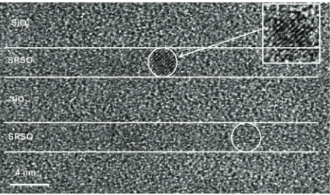
E. Talbot et al.
Fig. 1: (Colour on-line) High-Resolution TEM image of the SRSO/SiO2 multilayers. Two crystallized Si-nanoclusters are
revealed (white circles and magnified image (inset)).
Results and discussions. – Figure 1 shows a cross-sectional HRTEM image of the SRSO/SiO2 multilayers
(carried out on a Topcon 002B on samples prepared in the cross-section configuration). The presence of crystalline Si-nanoparticles in the SRSO sublayers is revealed (as shown in the inset) when diffraction conditions are fulfilled. These particles are only localised, as expected, in SRSO layers. Therefore, even with this high resolution technique, it is difficult: i) to estimate the particle number density and ii) to characterize nanoprecipitate/matrix interfaces. Complementary information is provided by high resolution analysis technique such as laser-assisted three-dimensional atom probe tomography (3D-APT). It is able to provide a spatial chemical map at the atomic scale [17]. The basic principle of the technique is the field evaporation of surface atoms. During the analysis, a high positive DC voltage (several kilovolts) is applied on the sample in order to create an electric field at the apex of the tip. The superposition of femtosecond laser pulses lead to the controlled evaporation of the specimen. The evaporated ions are collected on a position-sensitive detector which measure the time of flight of individual ions (time of flight mass spectrometry) and the impact position of each ion on the surface of the detector. These data permit the three-dimensional reconstruction of the analyzed volume at the atomic scale. A more detailed description of the principles of the technique may be found in references [18–21]. The recent development of this technique allows to carry out analyses of “poor” conductor materials by using laser-assisted evapor-ation [22]. In order to be a quasi-stereographic projection microscope and to locally increase the required electrical field and thus to perform 3D-APT experiments, the sample needs to be tip-shaped with a small cone angle and a radius of curvature of the extremity smaller than 50 nm. Such a requirement is achieved using an annular milling procedure with a focus ion beam (FIB) [23,24]. In order to prevent ion beam damages and gallium implantation, the samples were previously protected with a 300 nm Cr layer. The final steps of the process consist
m n 1 5 x 3 1 x 3 1 : x o B 3 i S O s i s y l a n A n o i t c e r i d
Fig. 2: (Colour on-line) 3D reconstruction of the SRSO/SiO2
multilayers analysed by LA-WATAP. Each dot represents one atom (Si or O). The volume is 13 × 13 × 51 nm3. SRSO layers are indicated by arrows and dashed lines.
in the milling of the tips at a low acceleration voltage (2 kV). The laser-assisted wide-angle tomographic atom probe (LA-WATAP) used in this work is a CAMECA version. The experiments were performed at 80 K, using UV (343 nm) femtosecond laser pulses (50 nJ, 350 fs) with a pulse repetition rate of 100 kHz.
Figure 2 shows a 3D reconstruction image of the SRSO/SiO2 multilayers analysed by LA-WATAP.
The stacking of the SRSO and SiO2 sublayers in the
growth/analysis directions is clearly visible. In the SRSO sublayers indicated by an arrow and dashed-line, a higher Si content is evidenced and in some parts, Si-nc can be detected. In order to visualize clearly the presence of the Si-nanoclusters, a 3D iso-concentration surfaces image, which map the Si-rich concentration zones, is performed and shown in fig. 3(a). This figure corresponds to the fig. 2 where areas with %Si > 75% are in red (i.e. Si-ncs) and areas with %Si = 33% (i.e. SiO2matrix) are in green. The
expected distribution of Si-nc (in red) in SRSO sublayers between pure silica sublayers (in green) is evidenced. The corresponding concentration profile in at.% along the growth direction of the multilayer is presented in fig. 3(b). The abscise axis corresponds to both growth and analysis direction while the y-axis give the atomic concentration in at.% of Si or O atoms. The measured atomic composition evidences the alternating stacking sequence of deposited nano-layers with pure silica sublayers (XSi≈ 34.3 ± 0.3
at.% and XO≈ 65.7 ± 0.3 at.%) separated by Si-enriched
regions (XSi≈ 51.0 ± 0.3 at.% and XO≈ 49.0 ± 0.3 at.%).
Thus the Si excess (%Siexcess= XSi(1 −12XXSiO) in the
3.8 nm thick SRSO sublayers is estimated to ∼26%. The Si-content in the SRSO sublayer is found to be XSi≈ 41.9 ± 0.3% (and XO≈ 58.1 ± 0.3%) which is
signif-icantly higher than a pure silica matrix (XSi= 33.3%
and XO= 66.7%). This local measured composition
n o i t c e r i d s i s y l a n A ) a ( m n 0 7 x 5 2 x 5 2 : e m u l o V 3 ) b ( i S O
Fig. 3: (Colour on-line) (a) 3D iso-concentration of the SRSO/SiO2 multilayers (red: Si-nc). (b) Composition profile
along the multilayer.
initial silicon excess has precipitated in Si-nanoclusters. The 1 h-annealing time of the SRSO/SiO2 multilayers
and/or the annealing temperature fixed here at 900◦C
are not long/high enough to ensure a complete phase separation of the system. This confirms the slow phase separation process at such a temperature as suggested by Iacona et al. [25], and confirmed by Wang et al. [26] who suggested continous phase separation process as function of annealing temperature.
The Si-nc/SiO2interface has been analyzed by Daldosso
et al. on composite Si-SiO2 layers [10]. They concluded
by means of XANES and EFTEM experiments on the presence of a diffuse interface of about 1 nm between Si-nc and the SiO2 host matrix. Figure 4(a) and fig. 4(b) show
nanoscale composition profiles across Si nanoclusters. The profile in fig. 4(a) evidences three regions: the first one (R1) is the core (∼3.2 nm) of the Si-nc where the Si concentration is constant and maximum (Xcore
Si ≈ 80 ± 3
at.%). The R2 region is composed of a substoichiometric silicon oxide shell (SiOy) where the Si concentration varies
from Xinterface
Si ≈ 80 ± 3 at.% (core) to XSiinterface≈ 30 ±
3 at.% (matrix) along ∼1.4 nm. Then, the last region (R3) is the silica matrix Xmatrix
Si ≈ 30 ± 3 at.%). The
presence of 20 at.% O in the core of the Si-nanoclusters is surprising and in contradiction with some previous experimental results where the nanoclusters are given as pure Si [10,13,25]. It is well known that APT analysis of phases with large different field of evaporation as it is the case with Si-nc in pure SiO2, leads to a local
magnification effect artefact [27]. This latter, when the
) a ( 3 R 2 R 1 R 2 R 3 R ) b ( ) c ( ) d (
Fig. 4: (Colour on-line) (a), (b) Composition profile across a Si particle in the analyse direction for a Si-nc. (c) Measured cluster concentration as function of cluster radius. (d) Size distribution of the Si-nc diameter in the SRSO layers.
particle is a low-evaporation-field (EL) phase embedded
in a high-evaporation-field matrix (EH), is responsible of
trajectory aberration of the ions during field evaporation process. The signature of the effect is the characteristic ellipsoidal shape of the clusters after 3D reconstruction as observed in fig. 3(a) and the concomitant increase of the number density of atoms (number of atoms per unit volume) in the nanocluster. In the case of Si-nc in SiO2,
the density is multiply by a factor 4. Thus, this effect affects the size of the particle in the x- and y-direction, i.e., perpendicular to the analysis direction. However, the
E. Talbot et al.
Table 1: Calculated apparent Si content (at.%) in a Si-nanoclusters with a radius of rnc= 1.6 nm and rnc= 2.0 nm, with τ = 30%
and ∆e thickness.
SiO2 SiOX- XSishell= 50% SiOX- XSishell= 75% Linear SiOX
∆e (nm) XSi ∆e (nm) XSi ∆e (nm) XSi ∆e (nm) XSi
rnc= 1.6 nm 0.4 81.7% 0.6 80.6% 1.6 81.6% 0.8 81.7%
rnc= 2.0 nm 0.5 81.7% 0.7 81.7% 2.0 81.6% 1.0 81.7%
depth extension of the particle (in the z- or analysis direction) is accurate up to the interatomic distance. This increase in the density is also due to the introduction of atoms from originally located at the interface into the particle. Thus, in our case, this leads to an over-estimation of the O concentration in the Si cluster present in the SRSO sublayers. This well known artefact (already observed in FeCu system for example) has been fully described and quantified by Vurpillot et al. [28]. When the difference between the field of evaporation of two phases: ϵ = 20% (where 100 ∗ EH/EL= ϵ + 1) a composition bias
of ∼25% may be observed [28]. This demonstrates that specific cares are needed in the interpretation of atom probe data.
Starting from the hypothesis that Si-nc are Si pure, as mostly expected in the optical amplifier devices commu-nity, the stoichiometry of the surrounding shell of Si-nc, silicon oxide (SiOy) with different values of y, has been
tested in order to make a correction of the local magni-fication effect and determine the exact composition of the interface. The model is simply based on the assump-tion that the cluster has a spherical shape (as seen with HRTEM images). Based on calculation from Vurpillot et al.[28] and Blavette et al. [29], the silicon concentration of the nanocluster is given by
XSi(r) = r3 ncρSi+ τ!(rnc− ∆e)3− rnc3 " ρSiO2X shell Si r3 ncρSi+ τ [(rnc− ∆e)3− rnc3 ] ρSiO2 , (1)
where rnc is the radius of the Si-nc, ∆e is the thickness
of the shell around the Si-nc, τ is the fraction of atoms belonging to the interface or the surrounding shell and artificially introduced into the clusters by the field effect, ρSi= 50 at./nm3and ρSiO2= 66 at./nm
3are, respectively,
the density of Si and SiO2, and XSishell is the mean Si
concentration of shell. Using this relation, the evolution of Si concentration in the Si cluster as a function of the cluster size is calculated and is reported in fig. 4(c) for τ = 30%. This value has been taken from Blavette et al. work in which experimental and model are fitting in the case of a difference of 20% in the field of evaporation of the two phases [29] which is the difference estimated in our case. In this case, only the shell thickness and mean Si concentration of the shell are tuneable para-meters. The experimental concentrations deduced from the reconstructed volume have also been reported on the same graph. The good correlation between the modelling curve and the experimental data confirm the different field
effect described below and the good estimate of artefact parameters. To go further in the determination of the local microstructure, three hypotheses have been tested to determine the chemical composition of the shell around the Si-nc i) a pure silica shell has been considered which corresponds to an abrupt interface between Si and SiO2,
ii) a sub-stoichiometric silicon oxide shell (SiOy) with two
different values of the Si content XSi= 50% or 75%, iii) a
silicon oxide shell with a Si gradient with XSi ranging
from XSi= 100% (near the core of the cluster) down to
XSi= 33.3% (near the silica matrix). Blavette et al. [29]
have demonstrated that, in the case of ϵ = 20%, the ad-atoms (in the clusters) from the surrounding matrix or interface cannot come from more than a thickness of 0.25 nm. To determine the composition of the surrounding shell of the Si-nc, we have calculated, for the different hypotheses, the thickness of the shell (∆e) which is able to reproduce the observed Si cluster concentration of about Xmeasured
Si ∼ 80 at.%. The cluster radius was taken to
rnc= 1.6 nm (according to the composition profile on
fig. 4(a)) and to rnc= 2.0 nm, which corresponds to the
maximum size of the Si-nc. The results are reported in table 1.
In these multilayers, the results of the modelling allows to eliminate the hypothesis of sub-stoichiometric oxide (hypothesis 2 with Xshell
Si = 75%) and the linear silicon
oxide shell (hypothesis 3), for which shell thicknesses of ∆e = 1.6 nm and ∆e = 0.8 nm, respectively, were obtained, which is not physically acceptable with the field evapora-tion process. The case of SiO2or SiOy(with XSishell= 50%)
shells give a better agreement with the composition profile of the Si-nc (fig. 4(a) and (b)). Moreover, we can note that the large shell thickness obtained in the case of sub-stoichiometric oxide with Xshell
Si = 75% evidences the
fact that rich-Si shell cannot explain the detected oxygen content in the Si-nc.
Finally an explanation and modelling of the composition profiles obtained through the Si-nc are coherent with the description of Si pure nanoclusters embedded in the silica matrix. The local magnification effect artificially introduces oxygen in the reconstructed particles and shows diffuse interfaces (substoichiometric compositions). The correction of this effect leads to the conclusion that Si-ncs are pure Si embedded in silica. Daldosso et al. [10] have recently demonstrated (using HR-EFTEM and modelling) that Si-nc could be surrounded by a stressed SiO2 shell,
interpretation is coherent with our results although atom probe is not able to detect stress, specifically in the elastic domain.
At the end, an accurate size distribution (corrected from apparent diffuse interfaces) of the silicon clusters (sub-nanometric detection) can be deduced from the 3D-APT technique (fig. 4(d)). The size ranges from 0.5 to 4.5 nm. The mean diameter is 2.9 nm and the nanoclusters number density is estimated to 5.7 ± 1.0 × 10¹⁸Si-nc/cm3.
Such result highlights the new capability of the 3D-APT to detect small Si-nc embedded in SiO2 compared to
other techniques (HRTEM, XRD, Raman spectroscopy, EFTEM. . . ).
In summary, Si nanoclusters array in SRSO/SiO2
multi-layers was investigated by 3D atom probe tomography. 3D-APT results show at the atomic scale the characteristics of the nanoclusters. In the fabrication condition reported here which are the conditions usually applied for the Er-doped SRSO layers, the phase separation is incom-plete. This is evidenced with a Si-supersaturation in the SRSO layers and a large scale distribution size of the nanoclusters. More important, it is shown the existence of an abrupt interface between the Si-nc and the matrix. The results described here are of primary importance for the understanding of the optical properties of future Si-based device as well as for their modelling. Thus, next steps of this work will be to deeply analyze the effect of higher annealing temperature (1000 and 1100◦C) on the
local microstructure of these multilayers before studying the rare-earth (Er3+, Nd3+)-doped SRSO layers. For this latter, such a powerful atomic scale technique will allow to give some correlation between the optical properties and the chemical surrounding of the rare-earth ions as well as the localization of these ions towards the Si nanocluster. This will lead to an optimization of the fabrication process and pave the way to the achievemen of net gain in such doped materials.
∗ ∗ ∗
This work was supported by the Upper Normandy Region and the French Ministry of Research in the framework of Research Networks of Upper-normandy. The authors would like to thank Dr F. Vurpillot for his technical help on 3D atom probe reconstruction.
REFERENCES
[1] Pavesi L., Dal Negro L., Mazzoleni C., Franzo G. and Priolo F., Nature, 408 (2000) 440.
[2] Canham L., Nature, 408 (2000) 411. [3] Polman A., Nat. Mater., 1 (2002) 10.
[4] Fiori A. T. and Ravindra N. M., J. Electron. Mater., 32(2003) 1043.
[5] Tiwari S., Rana F., Hanafi H., Harstein A. and Crabbe E. F., Appl. Phys. Lett., 68 (1996) 1377.
[6] Franzo G., Priolo F., Coffa S. and Polman A., Appl. Phys. Lett., 64 (1994) 2235.
[7] Kenyon A. J., Trwoga P. F., Federighi M. and Pitt C. W., J. Phys.: Condens. Matter, 6 (1994) L319. [8] Fujii M., Yoshida M., Y. Kanzana M., Hayashi S.
and Yamamoto K., Appl. Phys. Lett., 71 (1997) 1198. [9] Franzo G., Boninelli S., Pacifi D., Priolo F.,
Iacona F. and Bongiorno C., Appl. Phys. Lett., 82 (2003) 3871.
[10] Daldosso N., Luppi M., Ossicini S., Degoli E., Magri R., Dalba G., Fornasini P., Grisenti R., Rocca F., Pavesi L., Boninelli S., Priolo F., Spinella C. and Iacona F., Phys. Rev. B, 68 (2003) 085327.
[11] Ternon C., Dufour C., Gourbilleau F. and Rizk R., Eur. Phys. J. B, 41 (2004) 325.
[12] Gourbilleau F., Levalois M., Dufour C., Vicens J. and Rizk R., J. Appl. Phys., 7 (2004) 3717.
[13] Gourbilleau F., Dufour C., Madelon R. and Rizk R., J. Lumin., 126 (2007) 581.
[14] Garrido B., Pellegrino P., Garcia C., Navarro-Urrios D., Daldosso N., Pavesi L., Goubilleau F. and Rizk R., Appl. Phys. Lett., 89 (2006) 163103. [15] Gourbilleau F., Portier X., Ternon C., Voivenel
P., Madelon R. and Rizk R., Appl. Phys. Lett., 78 (2001) 3058.
[16] Garrido B., Garcia C., Seo S.-Y., Pellegrino P., Navarro-Urrios D., Daldosso N., Pavesi L., Gourbilleau F.and Rizk R., Phys. Rev. B, 76 (2007) 245308.
[17] Kellogg G. and Tsong T., J. Appl. Phys., 51 (1980) 1184.
[18] Cerezo A., Godfrey T. J and Smith G. D. W., Rev. Sci. Instrum., 59 (1988) 862.
[19] Blavette D., Bostel A., Sarrau J. M., Deconihout B.and Menand A., Nature, 363 (1993) 432.
[20] Blavette D., Deconihout B., Bostel A., Sarrau J. M., Bouet M. and Menand A., Rev. Sci. Instrum., 64(1993) 2911.
[21] Miller M. K., Atom Probe Tomography: Analysis at the Atomic Level(Springer) 2000.
[22] Gault B., Vurpillot F., Gilbert M., Vella A., Menand A., Blavette D. and Deconihout B., Rev. Sci. Instrum., 77 (2006) 043705.
[23] Thomson G. B., Miller M. K. and Fraser H. L., Ultramicroscopy, 100 (2004) 25.
[24] Larson D. J., Foord D. R., Perford-Long A. K., Liew H., Blamire M. G., Cerezo A. and Smith G. D. W., Ultramicroscopy, 79 (1999) 287.
[25] Iacona F., Bongiorno C., Spinella C., Boninelli S. and Priolo F., J. Appl. Phys., 95 (2004) 3723.
[26] Wang J., Wang X. F., Li Q., Hryciw A. and Meldrum A., Philos. Mag., 87 (2007) 11.
[27] Miller M. K., Cerezo A., Hetherington M. G. and Smith G. D. W., Atom Probe Field Ion Microscopy, edited by Miller M. K. (Clarendon, Oxford) 1996. [28] Vurpillot F., Bostel A. and Blavette D., Appl.
Phys. Lett., 76 (2000) 3127.
[29] Blavette D., Vurpillot F., Pareige P. and Menand A., Ultramicroscopy, 89 (2001) 145.