A Data Path for a Pixel-Parallel
Image Processing System
by
Daphne Yong-Hsu Shih
S.B., Electrical Engineering
Massachusetts Institute of Technology (1994)
Submitted to the Department of
Electrical Engineering and Computer Science
in Partial Fulfillment of the Requirements
for the Degree of
Master of Engineering
in Electrical Engineering and Computer Science
at the
Massachusetts Institute of Technology
October 1995
@Massachusetts Institute of Technology, 1995.
All rights reserved.
Signature of Author
Department of Electrical Engineering and Computer Science October 25, 1995
Certified by
4
S Charles G. Sodini
rofes of neeing and Computer Science
- Thesis Supervisor
Accepted by
\ .Frederic R. Morgenthaler, Chairman
Department Committee on Graduate Students
;,;ASSACHiUSETTS INSTT UT'E
OF TECHNOLOGY
JAN
2
9
1996
A Data Path for a Pixel-Parallel
Image Processing System
by
Daphne Yong-Hsu Shih
Submitted to the
Department of Electrical Engineering and Computer Science October 1995
In Partial Fulfillment of the Requirements for the Degree of Master of Engineering in Electrical Engineering and Computer Science
Abstract
The design and implementation of a data path for a pixel-parallel image processing system is described. In this system, memories and processors are integrated on dense arrays of processing elements, with each processing element storing and processing one pixel of an image. Large processing element arrays are composed of a modest number of chips, with each chip handling one block of pixels. If image data from an imager are directly transferred to the processing element array on a pixel-by-pixel basis, only one chip would be active at any time. Thus, to quickly transfer an image to the array and to efficiently utilize the array, data must be rearranged in real-time. The goal of this thesis is to implement an efficient data path for the system.
The design employs static random-access memory chips and field programmable gate arrays to perform the format conversion. The hardware is capable of storing 256 x 256 pixel images into a memory buffer and transferring data to the array during the vertical blanking period. Functionality of the hardware is verified with source of data from a camera as well as a host computer.
Thesis Supervisor: Charles G. Sodini
Acknowledgments
I would first like to thank Professor Charles Sodini for granting me this research opportunity, and for his guidance and encouragement since I joined his research group as a UROP student and throughout the course of my studies. I would also like to thank Robert Tamlyn and Andrew Ellenberger from IBM for their support.
Many thanks to Jeffrey Gealow, for being my mentor, for his willingness to share his knowledge with me, for the countless times he has helped me during the past three years. He has not only dedicated a lot of his time in my design problems, but also saved me from many nightmares on C/C++, latex, UNIX, classes, to name a few. I have greatly benefited from working with him. Thanks also to Frederick Herrmann for providing me with ideas and suggestions over the phone and email.
Next, I would like to acknowledge some of the people from whom I have received technical assistance during board layout. I am grateful to Jennifer Lloyd for her help with Allegro. She saved me from many frustrations from reading the Cadence documentation. I would like to thank Steven Decker for his help with Allegro as well, and for his patience in answering all my little trivial questions on video signals and board layout techniques. I would also like to thank Frank Honore at LCS for sharing his experience on laying out a surface mount board, Russell Tessier for his experience with FPGAs and Ignacio McQuirk for his help with the PROMs.
I would like thank Patricia Varley, for her assistance with purchase orders, office supplies, and the fax machine, also to Myron Freeman, for retrieving my directory containing the FPGA schematics (twice) from the backup tape!
I would like to further extend my gratitude to friends and colleagues here at MTL. I would like to thank Michael Ashburn not only for the soldering he did for my board, but also for his friendship and company in lab working at night; Michael Lee for all the advice on life, for saving my board from becoming a disaster, and especially for programming those PROMs; others that had given me support in their own way: Joseph Lutsky, Michael Perrott, Christopher Umminger, Tracy Adams, Raja Jindal, and Gary Hall (even though it was only for the last two weeks).
During my undergraduate years here at MIT, I met a group of wonderful friends at Baker, who have become a family to me. My sincerest thanks to Maia Singer for being the best roommate a person can ever have, for always watching out for me, for helping me figure out who I am; to Annette Guy and Sita Venkataraman for being such great friends, for always being there for me; to Marcie Black and Peter Trapa and many others (I cannot include them all here) for all their friendship and support.
Special thanks to Vincent Wong, for believing in me, for helping me get through my last year at MIT, for putting up with me. I am forever grateful for his love and understanding.
Finally I would like to thank my family. I would like to thank my grandparents for raising me and my brother, Jimmy Shih, for his encouragement. Most importantly, I thank my parents, Scott and Shiew-mei Shih, for providing me with the best education and for their unconditional love throughout my life. They have given me more than I could ask for.
Support for this research was provided in part by IBM and by NSF and ARPA (Contract #MIP-9117724).
Contents
1 Introduction
1.1 Background ...
1.2 Pixel-Parallel Image Processing System . . . .
1.3 Organization of Thesis . ... 2 Data Path Architecture
2.1 Image I/O format ... 2.2 Previous Work ... 2.3 Real-Time Images ...
2.3.1 Spatial Partitioning ... . .
2.3.2 Corner-Turning Problem ... 2.4 Design of Format Converter . ...
2.4.1 Memory Address Registers ... 2.4.2 Shufflers ...
2.4.3 Memory Buffer . ...
2.4.4 The Reverse Process . . . . 2.5 Data I/O ...
2.5.1 Camera and Display . ...
2.5.2 Testing through the Host Computer..
3 Hardware Implementation
3.1 Format Converters ...
3.1.1 Field Programmable Gate Arrays . . .
3.1.2 Memory Buffer Design . ... 3.1.3 Output Format Converter ... 3.2 PE Array Interface ...
3.3 Image I/O Unit ...
3.3.1 Camera and Display . . . . 3.3.2 VM Ebus ...
3.4 PCB Design ...
3.4.1 Data Path Board Layout ...
3.4.2 Dummy Test Board ... . .
15 15 16 17 19 19 20 21 21 23 24 24 28 29 30 31 31 32 33 33 33 42 42 43 44 45 46 47 47 49
4 Results 53
4.1 Testing . .. . ... .. ... . .. .... .. . .. .. . . . . ... 53
4.1.1 C locks . . . .. . 53
4.1.2 Programming FPGAs ... 53
4.1.3 Communication via VMEbus . ... 54
4.1.4 Wiring and Design Oversights . ... 55
4.1.5 Using Real-time Images ... 57
4.2 Demonstration ... 58
4.3 Ribbon Cable Delay ... 58
4.4 PROM Programming ... 60 5 Conclusion 61 5.1 Accomplishments ... 61 5.2 Future Work ... 62 References 65 A Hardware Schematics 67 B FSMs in the FPGAs 89
C Timing Diagrams for Format Converters 101
D Handshaking Protocol 107
E PAL on the Dummy Test Board 111
List of Figures
1.1 Pixel-parallel image processing system . . . . Three-dimensional representation of an image . . . . Associative parallel processor array . . . . Existing system with associative parallel processor ..
Spatial partition of an image ...
Corner-turning problem . . . . Storage pattern for an 8 x 8 MDA memory . . . . Functional modules of format converter . . . . Functional description of the MARs for storing data . Actual storage pattern ...
Memory address register for storing data . . . . Functional description of the MAR for accessing data Functional description of a shuffler . . . . Memory buffer implementation . . . . 2.1 2.2 2.3 2.4 2.5 2.6 2.7 2.8 2.9 2.10 2.11 2.12 2.13 2.14 2.15 2.16 3.1 3.2 3.3 3.4 3.5 3.6 3.7 3.8 3.9 3.10 3.11 3.12 3.13 3.14
MAR for storing processed data into output format converter .. Data Path Block Diagram ...
Dimensions of a non-interlaced image . . . . Hardware functional block diagram . . . . FPGA architecture ...
XC4000H IOB structure ... XC4000 CLB structure ...
FPGA functional block diagram for the input format converter . Implementation of a shuffler ...
Implementation of mask write logic for a word . . . . Timing diagram for storing data into SRAMs . . . . Timing diagram for accessing data from SRAMs . . . . FPGA functional block diagram for the output format converter Timing diagram for data transfer . . . . PE array interface ... Video Interface . .. ... . . .. ... . . .. . . . . .. . . VM E Interface ... . . . . . 19 . . . . . 20 . . . . . 21 ... . 22 . . . . . 23 . . . . . 24 . . . . . 25 . . . . . 25 ... . 26 . . . . . 27 . . . . . 28 . . . . . 29 . . . . . 30 . . . 34 .. . 34 .. . 36 .. . 36 . . . 37 .. . 39 . . . 40 . . . 41 . . . 41 . . . 43 . . . 44 .. . 44 .. . 45 .. . 46
3.15 3.16 3.17 3.18
Data path board layout ... Ten-layer stack ...
Clock lines for data path board . . Dummy test board layout ... 4.1 Reset Circuit ...
4.2 Signal delay measurements... A.1 Main schematic of data path board A.2 Schematic of VME connector block A.3 Schematic of VME interface block . . . A.4 Schematic of camera interface block . . A.5 Schematic of FPGA1 block... A.6 Schematic of memory buffer 1 block . . A.7 Schematic of clock buffer block . . . .
A.8 Schematic of configuration PROM block
A.9 Schematic of diff driver block on data pa A.10 Schematic of PE array connector block
A.11 Schematic of diff receiver block on data A.12 Schematic of display interface block . . A.13 Schematic of FPGA2 block ...
A.14 Schematic of memory buffer 2 block . . A.15 Main schematic of dummy test board . A.16 Schematic of data path board interface A.17 Schematic of diff receiver block on dumn A.18 Schematic of diff driver block on dummy A.19 Schematic of test plane on dummy boar B.1 INITAD - FSM for initializing the digiti
. . . . 48 . . . . 49 . . . . 50 . . . . 5 1 . . . . 56 . . . . 59 . . . . . 69 . . . . . 70 . . . . . 7 1 . . . . . 72 . . . . 73 . . . . . 74 . . . . . 75 . . . . . 76 Ith board . ... 77 . . . . . 78 path board . ... 79 . . . . . 80 . . . . 8 1 . . . . . 82 . . . . . 83 )lock . ... 84 ny test board . ... 85 board . ... 86 d . . . 87 zer .. . . . . B.2 BIRD - FSM for storing data from host to memory buffer 1 . B.3 SOFSOD - FSM for generating SOF and SOD markers in FPGA 1.. 96
B.4 CAMFSM - FSM for storing data from camera to memory buffer 1 96 B.5 TRANS - FSM for transferring data to PE array ... 97
B.6 ENCOBACK - FSM for initializing the encoder . ... 97
B.7 COUNTRUN - FSM for generating SOF and SOD markers in FPGA 2 98 B.8 BACKTRANS -FSM for transferring data from PE array and to display 98 B.9 BACKVME - FSM for transferring data from memory buffer 2 to host 99 C.1 Timing for storing data into memory buffer 1 . ... 103
C.2 Timing for transferring data from memory buffer 1 to PE array . . . 104
C.3 Timing for sending processed data from PE array to display .... . 105
D.1 Handshaking at start of frame ... 108
D.3 Handshaking at end of frame ... 110 E.1 FSM on dummy test board ... 111
List of Tables
4.1 XChecker Cable Connector ... ... 54
4.2 VME device memory and user memory mapping ... 55
A.1 Hierarchical tree in board schematics . ... 68
B.1 Functional description of the FSMs . ... 90
Chapter 1
Introduction
1.1
Background
Edge detection, smoothing and segmentation, and optical flow computation are com-mon low-level image processing tasks. Such tasks require high computational speed, but only modest memory. In conventional general-purpose computers, the memory and the processor are physically separated (i.e. each is a discrete module). Thus, the speed of the system is limited by the data transfer rate between the two modules. In addition, there is typically a large ratio of the number of memory words to the number of processors in the system, requiring sequential operations. This is unsuit-able for real-time image processing applications since the processing tasks typically require that identical operations be performed on each pixel.
Due to the massively parallel nature of low-level image processing problems, single instruction stream, multiple data stream (SIMD) machines are more appropriate for carrying out the requisite computation. These machines contain an array of proces-sors, where each processor is assigned to one pixel of an image and executes identical instructions. However, the Connection Machine [1] and other massively parallel SIMD supercomputers, which are designed for a broad range of applications, employ com-munication networks that are more sophisticated than necessary for low-level image-processing tasks. This high level of sophistication translates into an unacceptably high cost. Recently, a pixel-parallel image processing system has been proposed for real-time image processing at low cost [2]. In such a system the memory and the processor are integrated on the same chip, with one processor per memory. In the next section the pixel-parallel image processing system is described in more detail, and the goals of this thesis are defined.
Host Computer
Controlle
I I I II FE't ArrayPE
PE PE
'I-Imager -CADC
0
0 P 4 P4 E 0 0 CuProcessed
Images
Figure 1.1: Pixel-parallel image processing system
1.2
Pixel-Parallel Image Processing System
Modern VLSI technology allows for the integration of memories and processors in dense arrays of processing elements (PE), where a memory is tightly coupled to one processor. These PE arrays form the basis for a pixel-parallel image processing sys-tem [2]. Each PE stores and processes one pixel of an image. Figure 1.1 shows a block diagram of a pixel-parallel image processing system, which consists of a processing element array, a controller, a host computer and two format converters. Analog sig-nals from an imager are converted to digital sigsig-nals, then formatted and transferred to the PE array. Instructions from the host computer are broadcast via the controller
to all PEs. Then the processed data are reformatted for subsequent use.
Two integrated circuit architectures for the PE array have been considered. The first architecture, which consists of an associative parallel processor employing content addressable memory cells, has already been demonstrated. Very little logic is required for each PE in this architecture for performing mask-write and match-and-conditional-write operations, and these operations can be combined to accomplish more complex tasks. The second architecture, which is currently under development, is a fine-grained parallel architecture using conventional DRAM cells. In this architecture, the logic for each PE is integrated with a DRAM column on the same chip, thereby eliminating the need for a column decoder. In this way, architectures with high density and small memory cell size can be achieved. In the remainder of this section, the controller architecture and the goals of this thesis will be described.
The control path has been designed and developed to maximize the utilization of the PE array by avoiding run-time instruction computation. In this new approach, low-level instructions are generated by the host computer and stored in the controller
before processing begins. If an operation involves a run-time value, this value is used to select the appropriate sequence of instructions in the controller. In addition, with the PE array supporting direct feedback of its status, the performance of the system is significantly improved compared to a system using only run-time flow control [2]. The programming framework is developed using the C++ programming language in such a way that the details of the system architecture are transparent to the programmer. This fact allows the programmer to focus on the applications.
Thus far, the system is capable of executing instructions from the host computer. However, it lacks a path for real-time image data to flow into and out of the system. If the image data output from the A/D converter (see Figure 1.1) are directly transferred to the PE array on a pixel-by-pixel basis, only one PE would be active at any time. A more efficient utilization of the PE array requires a format conversion of the image data so that data can be transferred to the array in parallel. The focus of this thesis is to develop a data path composed of the appropriate format converters to realize real-time image processing.
1.3
Organization of Thesis
In this chapter the problems with using some of the existing computer architectures for real-time image processing were discussed. A low cost pixel-parallel image processing system, shown in Figure 1.1, was offered as a solution to these problems.
Chapter 2 begins with a brief discussion of previous work on the development of the data path architecture for the proposed pixel-parallel image processing system. It then considers the issue of image format and describes the design of the data path architecture in detail.
Chapter 3 describes the hardware implementation of the data path. In particular, the design issues and the choices made in the implementation of each functional block in the data path are considered.
Chapter 4 reports the testing procedures and results as well as the problems en-countered during testing. Finally, Chapter 5 summarizes the major accomplishments of the thesis and suggests directions for future work. The timing diagrams and the schematics for the printed circuit board are included in the appendices.
Chapter 2
Data Path Architecture
2.1
Image I/O format
One way to describe a digitized image is to view it as a three-dimensional block. The height and width of this block represent the size of the image, and the depth represents the number of bits in each pixel. Figure 2.1(a) shows an image with 4 bits per pixel. In typical graphic applications, video memories are used to partition the image block into bit-planes as shown in Figure 2.1(b), with one video memory chip storing one bit plane of the image. An A/D converter outputs image data one pixel after another in a serial fashion. However, if data are transferred into the PE array in such a serial fashion, only one PE is active at any time while the rest of the array remains idle. A more efficient memory utilization can be achieved if data are stored on a plane-by-plane basis. In other words, the least significant bit of all pixels enter the array first, followed by the second least significant bit and so on. Therefore, the format converters must be designed to address such a word-serial bit-parallel to bit-serial word-parallel conversion, known as the 'corner-turning' problem.
Pixel
Depth
(a) dimension (b) planar partition (c) spatial partition
Figure 2.1: Three-dimensional representation of an image rnrll II I I~ II II Ilu
In addition, the array is physically composed of several chips, each processing one portion of an image. Because of this fact, a spatial partitioning of the image exists, as shown in Figure 2.1(c). In order to transfer information quickly, data must be sent to all chips simultaneously. Since the goal of the data path architecture is to allow real-time data transfer to the PE array, compatibility between an incoming image and the image format required by the array is essential. Consequently, the format converters must be designed for efficient array utilization as well as efficient data transfer.
2.2
Previous Work
A first step in the development of a data path has been taken to demonstrate the I/O facility of an associative parallel processor employing content-addressable memory cells. The PE array using the associative parallel processor handles images with 32 x 32 pixels. The array is composed of four chips, one for each quadrant of an image. Shift registers are implemented at the end of the columns (see Figure 2.2). Four bits of data, one for each sub-array, are transferred simultaneously. Then, data are shifted into the array one row at a time. Thus, the array design requires a special format where four bits of data are grouped together. The first group contains the least significant bit of the first pixel in each quadrant, the second group the least significant bit of the second pixel, and so on. The second least significant bits are
grouped similarly. / 16 \ Data In shift registers
Figure 2.2: Associative parallel processor array
Figure 2.3 shows the existing demonstration system. Sequences of microtions are generated by the host computer and stored in the controller. These instruc-tions are then called by the host once processing begins. The data path hardware allows information to flow between the host and the array. It has on-board mem-ory to handle eight frames of images, successfully demonstrating the I/O facility of
Figure 2.3: Existing system with associative parallel processor
the processor. However, it lacks the capability to perform format conversions in real time. Pre-stored and pre-formatted images from the host are used instead of real-time images. Then the processed images are reformatted and displayed by the host.
2.3
Real-Time Images
The focus of this research is to provide a path for real-time images to be transferred to the PE array for processing. The data path architecture is designed for using the high-density parallel processor with DRAM cells as the PE array. Image sources are supplied by a black-and-white video camera. In this section, the spatial partitioning of the array is discussed for processing 256 x 256 pixel images. Then, the corner-turning problem is addressed.
2.3.1
Spatial Partitioning
Since the data path hardware deals with real-time images, the data output from the camera must be shuffled and stored in the memory buffer. The PE array then needs to access the shuffled data and process them before the camera outputs the next frame. One way to handle this problem would be to implement two frame buffers, where one buffer stores a frame of data while the other sends data of the previous frame to the PE array. However, such a design requires two sets of SRAM chips to implement the memory buffers. In addition to the extra hardware required, image processing would need to be interrupted to transfer data from the serial access memories (SAMs) located on the PE chips to the PE memories. These concerns motivate the pursuit of an alternative design, where the data is transferred only during the vertical blanking periods.
256
4
L-L I I I I I
Fgh
MMTIM IMMM
MEMME%.
ME mmý
I 1 10
EMEM
Emm
MEEMEM
-rFT-Q
---
--
----Figure 2.4: Spatial partition of an image
blanking period [3]. Each scan takes 63.56 ps, resulting in a vertical blanking period of 1.27 ms. To allow enough time for the SAMs to transfer data to the PE memories, data should be accessed from the memory buffer and sent to the array in less than 1 ms . A transfer rate of 40 ns per bit (25 MHz) is chosen (which will be considered in Section 2.5.1) so that if only one bit of data is transferred at a time and there are 8 bits per pixel, only images containing 3,125 pixels or less can be transferred to the array within the vertical blanking period. Because high-resolution images contain at least 256 x 256 = 65,536 pixels, a picture must be divided into several blocks so that more than one bit can be transferred at a time. Hence, for a design capable of handling images with 256 x 256 pixels, a picture needs to be divided into at least 65,536 + 3,125 = 21 blocks. Division into 32 blocks was chosen because it is a power of two. Since each high-density processor chip handles 64 x 64 pixels, sixteen chips are required to implement the PE array for processing 256 x 256 images. Thus, an image is spatially partitioned into thirty-two 64 x 32 blocks, as shown in Figure 2.4, where each processor chip handles two picture blocks.
A 128-bit SAM is implemented for every 64 x 32 pixels. However, these SAMs are implemented in such a way that divides a 64 x 32 block further into two 64 x 16 sub-blocks. Image data from the memory buffer are thus transferred to the array by loading the least significant bits of the first row of each picture block, followed by the sixteenth row, into the SAMs. After that, data from the SAMs are copied into the array. Then the least significant bits of the second row and the seventeenth row of each picture block are loaded into the SAMs then copied into the array, and so on. Therefore, the total amount of time required to transfer a frame of data to the array is the sum of the time required to load up the SAMs (64 x 32 pixels x 8 bits x 40 ns = 0.66 ms) and that required to transfer data from the SAMs to the array. For
one picture block 64
one
16
SAM one processor chipFigure 2.5: Corner-turning problem
simplicity, the time required to transfer data from the SAMs to the array is referred to as the 'array transfer overhead time'. Since the controller is designed to deliver instructions at 10 MHz (100 ns), and assuming that four instructions (400 ns) are required each time data are transferred from the SAMs to the array, the total 'array transfer overhead time' is 51.2 ps (16 rows x 8 bits x 400 ns = 51.2 ts).
The above calculation showed that by partitioning an image into 32 picture blocks, a complete transfer of one frame of a 256 x 256 image can be achieved in 0.71 ms (0.66 ms + 51.2 ps), which is within a vertical blanking period. Hence, the format converters must be designed to output 32-bit 'data groups' (one bit per block) so that data can be transferred simultaneously to the array (one bit to each SAM).
2.3.2
Corner-Turning Problem
As mentioned earlier, the format of data from a camera or any other imager must match that required by the PE array. An A/D converter outputs data one pixel after another. However, the PE array achieves higher utilization when image data are stored on a bit-plane by bit-plane basis (see Figure 2.5). This corner-turning problem can be solved by employing a multidimensional access (MDA) memory to temporarily store the incoming data. Such a memory can be implemented with conventional RAM chips [4].
Consider an 8 x 8 MDA memory. It can be constructed from eight 8 x 1 RAMs. Data are stored according to the following rule: bit B of pixel P is stored in bit-location B of memory chip B D P, where B E P indicates the bitwise EXCLUSIVE-OR of B and P. Conversely, bit-location B of RAM chip C stores bit B of pixel
B
E
C. Figure 2.6 illustrates the storage pattern for an 8 x 8 MDA memory. In otherwords, when applied to an 8 x 1 image with 8 bits per pixel, the first pixel is stored along the diagonal, then the bits for the second pixel are stored around the first pixel in a zig-zag fashion, and so on, with the last pixel stored along the other diagonal. In this way, as the camera outputs a pixel, all the bits can be stored during that
~L·----~--·----·---P 0a 0 0 0 S2 ,6615514 13312 2
r
chip 0
0f***02
67 455423 321 chip 157 46 64 M. 3, 20 chip2 147 5616502•
21
3ol chip 3 137 26 62515
4o]
chip4 1271361910 63 4i4 5o I chip5 235 24 15342 1 6o chip6 i2. 25 134 14315261
chip 7 Pb= bitbof pixel PFigure 2.6: Storage pattern for an 8 x 8 MDA memory
particular pixel clock period by going into separate RAM chips. Consequently, all the bits belonging to the same bit-plane can be accessed simultaneously by reading them out of separate chips.
2.4
Design of Format Converter
The storage pattern for the MDA memory requires the implementation of data shuf-fiers to rearrange the pixel bits before they are stored into the memory buffer and to rearrange the accessed data before they are transferred to the PE array. It also requires the implementation of different memory address registers (MARs) for each memory chip. Figure 2.7 illustrates the functional modules of the format converter for sending data to the PE array. It takes digitized image data as the input and produces formatted data which are properly grouped for transfer to the array. This section focuses on the design of both the shufflers and the MARs for this format converter. A brief description of the reverse process, used for sending processed data to a display, for the other format converter is also given.
2.4.1
Memory Address Registers
As the storage pattern in Figure 2.6 shows, data are not stored sequentially into the memory chips. A different addressing sequence is required for each chip. As image data arrive one pixel after another, only chip 0 maintains sequential addressing of its memory locations, from location 0 to location 7. For chip 1, memory location 1 is addressed first, followed by location 0, then location 3 and location 2. In other words, the address 'jumps'; the order of every two memory locations is switched. For chip 2, it is the order of every two sets of two consecutive memory locations that is switched.
Counter
Memory Address Register
Digitized data -I I
from camera
-
HE
-0
Formatted data
to PE array
Figure 2.7: Functional modules of format converter
This 'jumping' algorithm continues such that bits in pixel 0 to pixel 7 are stored in chip 7 with the order of the addresses reversed. One straightforward method for implementing such an addressing scheme is with the use of a counter. In particular, the counter outputs are changed accordingly for each MAR. Such an implementation is shown in Figure 2.8.
counter
IQ2 101 IQO
Q2 Q1 QO Q2 Q1 00 Q2
01
00 A2 Al AO A2 Al AO A2 Al AOaddress to chip 0 address to chip 1 address to chip 2 chip 0 6chip 1 chip 2 7chip 4 2chip 5 chip 6 3s 24 53 , 42 6 chip6
25
34 43 52 616 chip 7Figure 2.8: Functional description of the MARs for storing data
By treating each picture block as one "giant pixel unit", this addressing scheme can be extended to handle images with 256 x 256 pixels. Figure 2.9 shows the actual storage pattern. Each pixel in the picture is denoted by a block number in superscript, followed by a pixel number. The subscript indicates the bit number. For example, 3346 represents the 6th bit of the 34th pixel in block 3. Using thirty-two 16K (64 x 32 x 8 =
16, 384) x 1 memory chips, 32-bits of data can be accessed and transferred to the PE array simultaneously. The first 8 pictures blocks, block 0 to block 7, are shuffled and
One picture frame ( 64 ) ( 64 ) ( 4 ) U4 0 01 06 10 11 K 2 21 3 3 )4 '64 264 64 0 46154 & 40 e 0 7 b go 00 o 10 120 30 140 0 T6016 166 70171 1763 10181 186 90191 1 963 1654 765464 64 40 250 260 270
Figure 2.9: Actual storage pattern
Cm S Mem 0 Mem 1 Mem 2 Mem 3 Mem 4 Mem 5 Mem 6 Mem 7 Mem 8 Mem 9 Mem 10 Mem 11 Mem 12 Mem 13 Mem 14 Mem 15 Mem 16 Mem 17 Mem 18 Mem 19 Mem 20 Mem 21 Mem 22 Mem 23 Mem 24 Mem 25 Mem 26 Mem 27 Mem 28 Mem 29 Mem 30 Mem 31
Output of 16-bit Counter 113 112 Ill 110 19 18 17 16 15 14 13 12 11 10
11111111
013 012 011 010 09 08 07 06 05 04 03 02 01 00 Address to mem 0, 8, 16, 24 113 112 Ill 110 19 IS 17 16 15 14 13 12 11 10 013 012 O11 010 09 08 07 06 05 04 03 02 01 00 J, Address to mem 2, 10, 18, 26 113 112 Ill 110 19 18 17 16 15 14 13 12 11 10 013 012 011 010 09 08 07 06 05 04 03 02 01 00 I, Address to mem 4, 12, 20, 28 113 112 Ill 110 19 18 17 16 15 14 13 12 11 10013
012
010
09
08
07 050403020111111
013012 0110 09 06 07 06 06 04 03 02 01 00 Address to mem 6, 14, 22, 30 113 112 Ill 110 19 18 17 16 15 14 13 12 11 10I tC1111111
013 012011 010 09 08 07 06 05 04 03 02 01 00 J, Address to mem 1, 9, 17, 25 113 112 Ill 110 19 IS 17 16 15 14 13 12 11 10 013 012 011 010 09 08 07 06 05 04 03 02 01 00 Address to mem 3, 11, 19, 27 113 112 Ill 110 19 18 17 16 15 14 13 12 11 10ti
I
I11
013 012 011 010 09 08 07 08 05 04 03 02 01 00 J, Address to mem 5, 13, 21, 29 113 112 Ill 110 19 18 17 16 15 14 13 12 11 10i
I 1111 11
013 012011010 09 08 07 06 05 04 03 02 01 00 Address to mem 7, 15, 23, 31Figure 2.10: Memory address register for storing data
stored in the first 8 memory chips. The data storage rule is modified as follows: bit
B of pixel P of block U is stored in bit-location B x (64 x 32) + P of memory chip B
E
U, where B x 2048 + P indicates the SUM (not bitwise OR) of B x 2048 and P. Conversely, bit-location B x 2048 + P of RAM chip C stores bit B of pixel P ofblock B
e
C. For example, for memory chip 0, as the camera outputs pixels 00 to063, 10 to 163, and 20 to 263, the MAR must count from 0 to 63, 2048 to 2111, and 4096 to 4159, respectively. This semi-sequential addressing order can be achieved by rearranging the order in which the counter outputs are wired to the memory address inputs as illustrated in Figure 2.10. For memory 1, the addresses 'jump' even more. One of the bits from the counter needs to be inverted. The addresses for the other memory chips can be generated by different rearrangements of the counter outputs. Although Figure 2.10 shows only eight different MARs, they are used for memory 8 to 15, 16 to 23, and 24 to 31 as well.
Accessing data from the memory buffer is less complicated. In the case of an 8 x 1 image, all the bits belonging to the same bit-plane can be accessed from the same memory location. Thus, only one addressing sequence is required to address all chips, and the addressing order is sequential. In particular, all bits in bit-plane 0 are in location 0, bit-plane 1 in location 1, and so on. Similarly, only one address sequence
is required for accessing data from the memory buffer for 256 x 256 pixels. However, the memory locations cannot be addressed sequentially. This is due to the design and implementation of the SAMs in the high-density parallel processor. Each of these SAMs contains 128 registers, thereby dividing each picture block further into two sets as shown in Figure 2.4. Therefore, when transferring each picture block to the array, every row in the first sixteen rows must be followed by the corresponding row in the second set. This requires a 'jump' in the order of the address. The corresponding bit rearrangement is shown in Figure 2.11.
Output of 16-bit Counter
113 112 11l 110 19 18 17 16 15 14 13 12 I1 10
013 012 011 010 09 08 07 068 05 04 03 02 01 00
4,
Address to all memory chips
Figure 2.11: Functional description of the MAR for accessing data
2.4.2
Shufflers
The previous section described the sequences for addressing the proper memory lo-cations. However, in order to achieve the actual storage pattern shown in Figure 2.9, the bits within the pixels need to be rearranged as well before they are stored into the memory buffer. In other words, for storing image data into the memory buffer, both the pixel bits and the memory addresses need to be shuffled. (The data shuffling pattern turns out to be rather simple.) The eight bits of each pixel in block 0 are stored in the corresponding eight memory chips. However, for pixels in block 1 , every two bits are switched. For example, bit 0 is stored in chip 1, and bit 1 is stored in chip 0. For block 2, every two 2-bit groups are switched. The switching pattern continues so that for block 7, the order is reversed with bit 0 stored in chip 7 and bit
7 in chip 0 (see Figure 2.6).
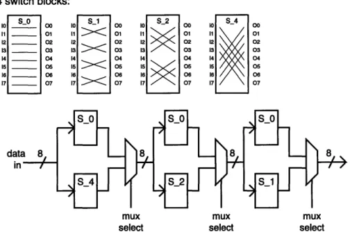
A total of 8 different shuffling patterns are required for storing data into the memory buffer; however, functionally, they can be generated by the appropriate com-bination of only 4 different switching blocks as shown in Figure 2.12. Switch block
S_0 leaves the order of the data unchanged; S_1 switches every 2 bits; S_2 switches
every two 2-bit groups; and S.3 switches the two 4-bit groups. The desired patterns are selected by the inputs to the multiplexers.
Although the storage pattern allows easy access of bit-planes, it requires that the bits within the bit-planes be reordered. Therefore, another shuffler at the memory output is required for sending data to the PE array. A careful look at the storage
4 switch blocks: S S_0 o0 IO S12 S 11 01 11
[ 7
01 13 01 11 01 12 02 12 02 12 02 12 02 13 03 13 03 13 03 13 03 14 04 14 04 14 04 14 04 15 O 15 05 15 05 15 05 16 06 16 06 16 06 16 06 17 _ 07 17 < 7 17 07 17 07 7 7mux mux mux
select select select
Figure 2.12: Functional description of a shuffler
pattern will show that the second shuffler can be implemented in the same way as the one just described. Functionally, both shufflers are identical.
2.4.3
Memory Buffer
Conceptually, the memory buffer described earlier requires 32 separate memory chips, each with a 1-bit bus. If SRAMs with buses of more than 1 bit are used, the number of chips required and, consequently, the system cost can be greatly reduced. Using eight 16K x 4 SRAM chips, the memories can be grouped as shown in Figure 2.13. As the camera outputs a pixel, all eight bits can be stored into eight physically discrete chips. Such utilization of the SRAMs is not a problem for data access since the same memory addresses are used for all chips; however, it does become a problem during data storage. Each time a write cycle is performed for storing a pixel into a SRAM chip, all four bits in that particular location are modified. Thus, the format converter must be designed with the capability of 'mask writing' data into the memory buffer. In other words, during each pixel clock period, the format converter needs to perform a read cycle, modify only one bit in a word, and write the result into the same memory location. In this way, picture block 8 to 15 can be shuffled and stored in memory 8 to 15 while keeping the information in picture block 0 to picture block 7, which are stored in memory 0 to memory 7.
8 pixel bits
size of each SRAM chip
= 16Kx4 SRAM chip 0 SSRAM chip 1 S SRAM chip 2 --z iSRAM chip 3 SzSRAM chip 4 -SRAM chip 5 S SRAM chip 6 -- SSRAM-- chip 7
Figure 2.13: Memory buffer implementation
2.4.4
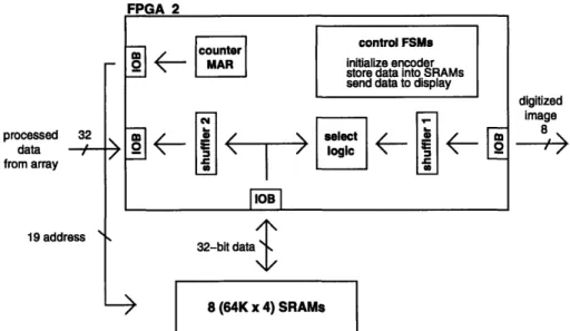
The Reverse Process
There are two format converters in the data path hardware, one for sending image data from the camera to the PE array, the other one for shuffling the processed data and sending them to a display. For clarity and simplicity in the discussion that follows, the former will be referred to as the 'input format converter' and the latter the 'output format converter'.
The output format converter can be implemented by reversing the shuffling process as described in the previous section. The same data shuffling patterns are used here, and the same addressing sequences as shown in Figure 2.10 are used for reading data out of the memory buffer. However, the MAR for storing data into the memory buffer is slightly different from the one shown in Figure 2.11. The high-density parallel processor chips are not designed to transfer a frame of processed data to the output format converter in the same order that they receive data from the input format converter. The MAR is functionally implemented as shown in Figure 2.14. The SAM in each processor chip shifts out data in row 15 followed by row 31, row 14, row 30 and so on.
Output of 16-bit Counter
113 112 Ill 110 19 18 17 16 15 14 13 12 11 10
013 012 011 010 09 08 07 06 05 04 03 02 01 00
Address to all memory chips
Figure 2.14: MAR for storing processed data into output format converter 30 Mem Mem Mer 16 Mem 24 Mem 1 Mem 9 Mem 17 Mem 25 Mem 2 Mem'n Mem 311 Mem 19 Mem 27 Mem28 21 e29 em 6 em 14 em 22 Mem 30 Mem 7 Mem Mem 1523 Mem 31
Counter
IMemory Address Registerl
Camer
~~.Gitizer2m~mKi~lsr~0-F"c
Host VME
Computer -* Interface
Si
Encoder
Counter
Memory Address Regis
SRAMs - memory buffer
CD
1t1 PE Array P PE terl 2I~i
<--216-4-Figure 2.15: Data Path Block Diagram
2.5
Data I/O
The overall block diagram for the data path architecture is shown in Figure 2.15. Images from a camera are converted to digital data and shuffled before being stored in the memory buffer. Then, they need to go through another shuffler before being transferred to the PE array for image processing. The reverse process is done for sending processed data from the PE array to a display. For testing purposes, images from the host computer are used.
2.5.1
Camera and Display
In standard television and video systems, the vertical scanning frequency is 60 Hz and the horizontal scanning frequency is 15.75 KHz. The aspect ratio, the width-to-height ratio of the picture frame, is standardized at 4:3. Because motion in a video is usually in the horizontal direction, the frame is made such that the width is greater than the height [3]. For non-interlaced scanning, this scanning configuration translates a frame of an image into a rectangular picture as depicted in Figure 2.16. The shaded area represents the active video, and the white area represents the vertical and/or horizontal retraces. A Sony CCD black-and-white video camera capable of operating in both interlaced and non-interlaced modes is chosen as the main source of image input [5]. However, because the PE array handles 256 pixels in the horizontal direction, only part of the picture in the horizontal direction is needed. Every other pixel is shuffled and stored in the memory buffer. In the vertical direction, the PE array will process a few lines of invalid video data due to the availability of only 242
20i lines 242 lines vertical blanking I... NTSC pixel clock = 12.27MHz 646 pixels Active video
-. Data processed by PE array (256 pixels x 256 pixels)
Figure 2.16: Dimensions of a non-interlaced image lines of image.
Since the focus of this research is on the design and implementation of the format converters, a Raytheon video digitizer chip containing an A/D converter and all the proper analog filters is chosen for converting analog signals from the camera to digital data. The chip can be programmed for NTSC operation and is capable of extracting horizontal and vertical sync signals. It generates a pixel clock of 12.27 MHz for the on-chip 8-bit A/D converter and a 2X pixel clock (24.54 MHz). This 2X pixel clock is chosen for running the entire data path hardware, thereby avoiding synchronization problems among different functional modules such as the shufflers, the interface with the VMEbus, and the interface with the PE array. Thus, the rate for transferring data to the PE array is approximately 25 MHz as mentioned in Section 2.3.1.
A Sony Trinitron color video monitor is chosen as the display since it was readily available. Image output data are converted to analog signals for display by using a Raytheon video encoder chip. The chip can be synchronized to the Raytheon digitizer chip described earlier and is capable of providing the proper composite signal, containing only the luminance component, for the monitor.
2.5.2
Testing through the Host Computer
Another data input is provided by the host computer for testing the data path hardware. Data transfer via the VMEbus is chosen because it has a relative high bandwidth (i.e. 32 bits can be transferred at a time at the rate of approximately 7 MBytes/second) [6]. The hardware required for the bus interface can be easily implemented with a PLX VME2000 chip. In addition, the VMEbus adaptor for the host computer (a Sun SPARCstation), the VMEbus backplane and the chassis were already available from the development of the controller for the pixel-parallel image processing system.
"'~
V
Chapter 3
Hardware Implementation
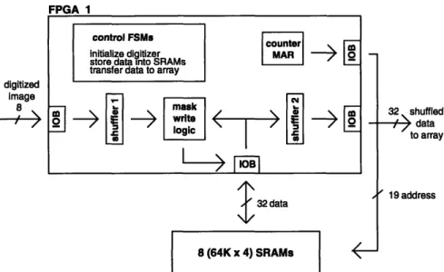
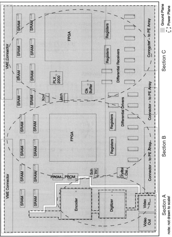
This chapter describes the hardware implementation of the data path architecture. The circuit board consists of the four functional blocks shown in Figure 3.1: one image I/O unit, two format converters, and one PE array interface. The image I/O unit contains the interface with the camera, with the display and with the VMEbus. In each format converter, eight SRAMs are used to implement the memory buffer and a field programmable gate array (FPGA) is used to implement the shufflers and the MARs. Differential drivers and receivers are used in the PE array interface and data are transferred to and from the PE array via twisted-pair ribbon cables. The implementation of the image I/O unit, the PE array interface and the layout of the printed circuit board are described. The focus for this chapter, however, is on the format converters, more specifically the FPGAs, which are instrumental in the realization of real-time image processing. The schematics for the data path hardware are included in Appendix A.
3.1
Format Converters
As shown in Figure 3.1, there are two format converters in the data path. The follow-ing section will first describe the implementation of the input format converter and the timing for the signals involved. Then a brief description on the implementation of the output format converter will given.
3.1.1
Field Programmable Gate Arrays
FPGAs are electrically programmable devices just like the traditional programmable logic devices (PLDs). However, they have the capability to implement far more com-plex logic than just the 'sum-of-product' logic capable of the PLDs. The architecture of a FPGA is similar to that of a mask-programmable gate array (MPGA), which consists of an array of logic blocks and interconnections. (See Figure 3.2.) These
Figure 3.1: Hardware functional block diagram
interconnections contain switches that can be programmed for realizing different de-signs. Due to the fact that switches and the programmable routing resources are pre-placed, it is very difficult to achieve high density and a 100% logic utilization. Thus, FPGAs are suitable for rapid prototyping of only small and medium size ASIC design. In addition, the performance of a FPGA-based design probably falls short of a custom ASIC. Nonetheless, in this research, such a design approach is taken for economic reasons. (More information can be found in an article on FPGAs in IEEE
Potentials [7].)
Interconnection Resources
Configurable Y -- I/0 Block
Logic Block
Background and Choices
Several programming technologies exist for programming the switches in the FPGAs. An article in Proceedings of the IEEE [8] discusses three of the most commonly used, the SRAM, antifuse, and EPROM programming technologies. SRAM programming technology uses pass transistors to implement the switches which are controlled by the state of the SRAM cells. Devices from Xilinx use such a technology. In antifuse programming technology, the antifuses serve as switches. These switches form low resistance paths when electrically programmed. The advantages of the antifuses are their small size and their relatively low series resistance and parasitic capacitance. However, an FPGA employing this programming technology, such as those from Ac-tel, is not re-programmable. In EPROM programming technology, the switches are implemented by floating-gate transistors. A switch is disabled by injecting charge onto the floating gate. Such an implementation is used in Altera FPGAs. As with the SRAM programming technology, the EPROM technology is re-programmable. However, EPROMs have higher ON resistance than the SRAMs and they are ultravi-olet erasable instead of electrically erasable. Although EEPROM-based programming technology, which is used on AMD and Lattice FPGAs, exists where the gate charges can be removed electrically, the size of an EEPROM cell is roughly twice that of an EPROM cell. Given the above design considerations, FPGAs from Xilinx were chosen for the data path hardware because of their density and fast re-programmability. In addition, Xilinx FPGAs are widely used at the MIT Laboratory of Computer Science. As shown in Figure 3.2, the Xilinx FPGA architecture consists of input/output blocks (IOBs) along the perimeter, a core array of configurable logic blocks (CLBs), and interconnection resources. The IOBs on the FPGA device provide an interface between the actual package pins and the internal CLBs. Xilinx offers three families of FPGA devices, the XC2000, XC3000, and XC4000 families. Two XC4005H devices are used since each one has a large number of CLBs and I/O pins, which are enough for implementing the logic required for either format converter. In addition, the 'H' family is intended for I/O intensive applications. It offers an improved output slew-rate control that reduces ground bounce without any significant increase in delay. A more detailed description can be found in the Xilinx FPGA data book [9]. The package is a ceramic PGA with 223 pins of which 192 are I/O pins. Figure 3.3 shows the I/O block structure of the Xilinx 4000H family. Each output can be inverted, tri-stated, or tri-state inverted, and the slew-rate can be controlled. Configuration options on the inputs include inversion and a programmable delay to eliminate input hold time. (The XC4000H devices differ from the XC4000 and the XC4000A in that the IOBs for the XC4000 and the XC4000A devices contain input and output registers.)
The CLBs provide the functional elements for constructing the user's logic. The architecture for a logic block in the XC4000 families is shown in Figure 3.4. There are two four-input function generators (G and F), or look up tables, feeding into a three-input function generator (H). There are two outputs in each CLB (X and Y).
Figure 3.3: XC4000H IOB structure
Cl C2 CS C4
MULTIPLEXER CONTROLLED BY CONFIGURATION PROGRAM
FPGA 1
control FSMs
initialize digitizer MAR
store data into SRAMs transfer data to array digitized
m 0
...=5m .
ewrite K... g ic II BI 32 data 8 WAIF
v dA COAll 32 shuffled - data to array 19 addressFigure 3.5: FPGA functional block diagram for the input format converter Signals from function generators F, G, and/or H can be output directly or stored in registers XQ and YQ. Thus, a CLB is capable of implementing either two independent functions of four variables, or any single function of five variables, or any function of four variables together with some functions of five variables, or even some functions of nine variables. The FPGA design in this research involves the implementation of wide functions in a single CLB to reduce both the number of CLBs required and the delay in the signal path, thereby achieving not only the functionality of the format converter but also an increase in density and speed.
Design
Figure 3.5 shows the main functional blocks inside the FPGA for the input format converter. Digitized image data are rearranged by the shuffler on the left (shuffler 1) during the active video period. As discussed in Section 2.4.3, this format converter must be capable of performing 'mask write' operations. Thus, while an image pixel is being shuffled by shuffler 1, eight words must be read out of the SRAMs and into the mask write logic block. In this way, the shuffled image data can be successfully stored into the memory buffer in their proper bit locations. Then, during the vertical blanking period, data are read out of the memory buffer and rearranged further by shuffler 2. The results are sent to the PE array. The memory addresses are generated by a counter as described in Section 2.4.1. The FSMs are responsible for all the control signals, in particular, for initializing the video digitizer, storing data into the SRAMs and transferring data to the PE array.
The most direct way to implement a shuffler is to cascade three stages of multiplex-ers, as shown in Figure 2.12. In other words, each stage contains eight 2:1 multiplexers with the first stage achieving the equivalent functionality of either switch block S_0
or S_4, the second stage either S_0 or S_2, and the third stage S_0 or S_1. This is shown in Figure 3.6(a). Since there are four inputs to both the F and the G function generators in each CLB, the multiplexers can be grouped so that a shuffler uses a total of twelve CLBs. However, such an implementation does not utilize the H func-tion generator in the CLB. An alternative design can be achieved with a two-stage implementation as shown in Figure 3.6(b). The 4:1 multiplexers in this implementa-tion utilize the H funcimplementa-tion generators and accomplish the equivalent tasks of stage 2 and 3 in the three-stage implementation, reducing the propagation delay. For an XC4005H-5 FPGA, the delay from the F/G inputs to the X/Y outputs is 4.5 ns and from the F/G inputs via H to the X/Y outputs is 7.0 ns. Thus, the delay in the 4:1 multiplexers in the two-stage implementation is 7.0 ns, where as the combined delay in stage 2 and 3 in the three-stage implementation is at least 9.0 ns (since the delay on the wire segments between two CLBs must be taken into consideration).
In the mask write logic block, a 2:1 multiplexer is used for each bit in a word. Each multiplexer selects either the original word bit from the SRAM or the shuffled data from the shuffler, as shown in Figure 3.7. Elementary logic gates are used to implement a two-line to four-line decoder to control the select inputs. This ensures that, for each word, only one bit is modified. The multiplexers and the AND gates map nicely into the four-input F and G function generators so that only sixteen CLBs
are required to implement the mask write logic for 32 bits of data.
Each XC4005H FPGA contains 196 CLBs and 192 IOBs. The format converter design requires approximately 80% of the CLBs and 70% of the IOBs for implementing the shufflers and the mask write logic as well as the memory address registers and
the FSMs. The FSM state-transition diagrams are included in Appendix B.
Timing
As mentioned in Section 2.3.1 the timing associated with the path from the memory buffer through shuffler 2 to the PE array is critical since a frame of data must be transferred to the PE array within the vertical blanking period. A further look at Figure 3.5 shows that the timing associated with the path from the camera through shuffler 1 and the mask write logic is also critical. The timing diagram for storing image data into the SRAMs is shown in Figure 3.8. The input format converter has approximately 160 ns to store a shuffled pixel into the memory buffer. (The camera outputs data at a rate of 12.27 MHZ, which translates to 80 ns, but only every other pixel is shuffled by the input format converter.) However, in those 160 ns, the FPGA must generate the memory address, read a word from each SRAM, modify only one bit of a word and then write the results into the SRAMs. Because the FPGA is running with a 25 MHz clock (40 ns-period), the delays through shuffler 1, the mask write logic block and the IOBs become significant. In the actual design, both shufflers employ the two-stage implementation and are pipelined with registers placed after stages 1 and 2. Registers are placed after the multiplexers in the mask write logic block as
stage 1 stage 2 stage 3 XO aO aO bO bO YO X4 F a2 F bi F Xl al al bl bl Y1 X5 G 3 G b G X2 a2 a2 b2 b2 Y2 X6 aG b3 X3 a3 a3 b3 b3 Y3 X7 al b2 X4 a4 a4 b4 b4 Y4 XO a6 b5 X5 a5 a5 b5 b5 Y5 Xl a7l -- b4 X6 a6 a6 b6 b6 Y6 X2 a4 b7 X7 a7 a7 b7 b7 Y7 X3 a5 b6 ... ... .. .. .
select 2 select 1 select 0
(a) three-stage implementation
stage 1 XO aO X4 F X1 al X5 G X2 a2 X6 X3 a3 X7 X4 a4 XO0 X5 a5 X1 ... X6 a6 X2 X7 0 a7 X3 select 2 stage 2 aO al YO a2 a3 al aO Y1 a3 a2 a2 a3 Y2 aO al a3 a2 Y3 al aO a4 a5 Y4 a6 a7 a5 a4 Y5 a7 a6 a6 a7 Y6 a4 a5 a7 a6 Y7 a5 a4 select 1 select 0
(a) two-stage implementation
Figure 3.6: Implementation of a shuffler
12 CLBs
3 Levels
12 CLBs 2 Levels
oldbitO newbitO oldbitl newbitl from SRAM oldbit2 - - newbit2 oldbit3 - newbit3
sell selO shuffled
pixelbit (from shuffler)
Figure 3.7: Implementation of mask write logic for a word
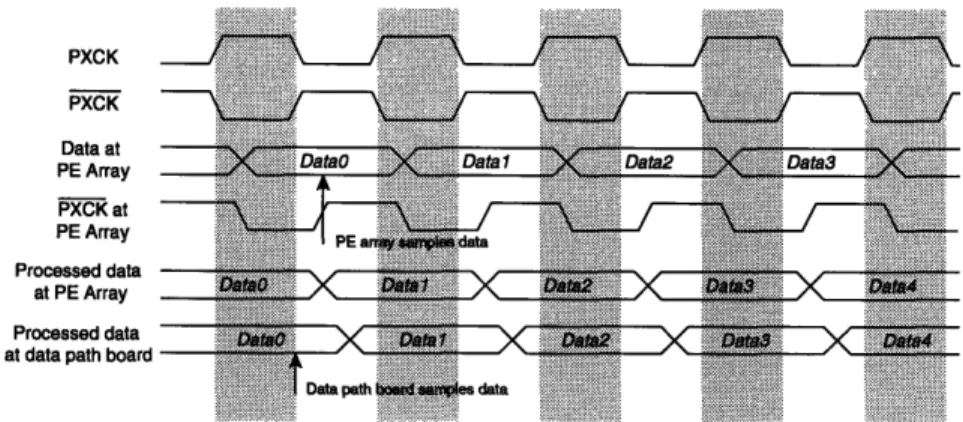
well. CLK2 is used for clocking these registers so that the data output of the FPGA to the SRAMs are valid. The timing for accessing data out of the SRAMs during the vertical blanking period is straightforward, as shown in Figure 3.9. The FPGA generates the memory addresses for reading data out of the SRAMs. The data are then latched by the registers inside the FPGA and the shuffled data appear two clock cycles later for transfer to the PE array. The process is pipelined.
Programming
A Xilinx FPGA design can be started either in a hardware description language or in a schematic editor. In this research the schematics are drawn with the Viewlogic CAD tool, Viewdraw, on a Sun SPARCstation. Simulations can be performed after this stage for functional verification. The completed design is then translated into a format compatible with the FPGA by the partitioning, placing and routing program. The users can control the placing and routing of the design to a certain degree by specifying the physical location of the CLBs and timing specifications between flip-flops, from flip-flops to I/O pads and from IO pads to flip-flops in schematics. Timing simulations are performed before the FPGA is programmed. Although SRAM programming technology used in FPGAs from Xilinx yields fast re-programmability, information stored in the devices is volatile. Thus, the FPGA must be re-configured each time the chip is powered-up. For testing and debugging, the configuration bitstreams can be easily loaded into the device via a serial port using the Xilinx XChecker cable. However, after in-circuit verification of the design is completed, an external permanent memory such as EPROM is required to provide the configuration bitstreams upon power-up. Xilinx supports one-time programmable bit serial read-only memories for this purpose. Hence, the data path hardware needs to be constructed with a connector for the XChecker cable as well as sockets for the serial PROMs.
CLK (PXCK) Data at FPGA Data C LK 2 i:·:+ -. .. . :: : ::: : : vo EN
Figure 3.8: Timing diagram for storing data into SRAMs
CLK ADD Data from SRAMs
at FPGA i
Data latched In FPGA to shuffler 2 Data out of FPGA
to Array
data 0 data 1 data 2 = data. = data 4
1-data 0 F-data 1 1-data 2 i-data 3 f-data 4
data out0 i data outi
Figure 3.9: Timing diagram for accessing data from SRAMs AddO Addl Add2 Add3 Add4