XV. CIRCUIT THEORY AND DESIGN
Prof. H. J. Zimmermann Prof. R. P. Rafuse L. O. Chua Prof. C. L. Searle Prof. R. D. Thornton L. G. Roberts Prof. J. W. Graham R. S. Badessa B. K. Vann, Jr.
D. A. Brown
A. CIRCUIT SIMULATION ON A DIGITAL COMPUTER 1. Introduction
In an attempt to simplify electronic circuit analysis, a program has been written for the TX-2 computer at Lincoln Laboratory, M. I. T., which will simulate the action of electronic circuits. The elements of the simulated circuits may be ideal resistors, capacitors, inductors, diodes, batteries, dependent sources, or models of other ele-ments that follow some mathematical law. These elements may be put together to form a circuit of reasonable size by typing their names and values into the computer. The values of components can be varied during the simulation and any voltage or current in the circuit can be observed on the computer display.
There are many methods of solving circuit problems that could be programmed for a computer to produce a circuit's response to various inputs. One approach is to deter-mine and solve the set of equations that specifies the circuit. This method offers the advantage of working with symbolic quantities as well as numbers, but it results in the same difficulty that human beings have with transcendental equations. Even when the equations are reasonable, this type of calculation is not efficient for a computer and tends to be very slow. Therefore, to produce a system capable of simulating almost any circuit at a reasonable rate, we decided to use a technique that is better adapted to computers - that of iteration at successive time intervals.
This method for simulating a circuit is based upon piecewise linear capacitors and inductors that act as biased resistors during each iteration period and change their bias only between iterations. Thus, during the iteration period the circuit is completely composed of sources, linear resistors, and nonlinear resistors such as diodes. The iteration procedure quickly converges upon a solution to the currents and voltages in the static circuit, and then the capacitors and inductors are adjusted for the next time interval. This procedure is repeated continually and the voltages and currents that are of interest are examined between iterations. The complete operation is under the con-trol of several constants on the computer console which concon-trol element values and an input voltage waveform. Hence, a network's response to some input waveform can be
examined as the network parameters are changed. The approximation of the capacitors
This work was supported in part by Purchase Order DDL B-00306 with Lincoln Laboratory, a center for research operated by Massachusetts Institute of Technology with the joint support of the U. S. Army, Navy, and Air Force under Air Force Contract
and inductors as piecewise linear elements is very good if the basic time interval is short compared with the reaction time of the circuit. Since the time interval is also variable at the console, the accuracy can be maintained at a high level.
2. Simulation Procedure
There are two basic methods of satisfying the currents and voltages in a circuit: either current or voltage can be used as the independent variable. Current was chosen as the independent variable for this program because of the simplicity of working with series elements in a computer. Thus, each element must be capable of computing a voltage to correspond to any current. At each node, a branch current coming in is split between the remaining branches in such a manner that the voltages generated by the branches are equal. To accomplish this, several iterations may be required. At each source, such as the input and supply voltage points, test currents are originated and varied until the voltage generated by the circuit in response to the test current is equal to the source voltage. When all source and node voltages are balanced, the iteration ceases and the energy-storage elements are adjusted for the next time interval.
In order to describe the simulation process more precisely, it is necessary to under-stand the structure of the actual computer program. Basically, the circuit is the pro-gram. If no circuit has been typed in, there is only a small program for input and output. The rest of the program will consist of small blocks of instructions, called
"macro instructions," one of which is introduced for each element of the circuit. A macro instruction is defined for each type of element and given a name, for example, RES for a resistor. Every time the name is typed, the block of instructions
corre-sponding to that name is added to the program. Following each name, the element value is typed: for example, RES = 500. If the element value is taken from one of the variable registers on the computer console it should be typed RES = POT1 x 1000 to indicate that the number in digital potentiometer No. 1 is to be multiplied by 1000 and used as the resistance value. The format for indicating the element value and the instructions necessary for its calculation are included in the definition of the element name. The macros for all of the circuit elements are compiled and stored in the computer memory by the assembly program Mark IV, at which point the simulation operation begins.
Since a computer operates instructions in a serial manner, only one part of the pro-gram can have control at any one time. Thus, in the simulation program, control is passed from macro to macro with each macro carrying out whatever calculations are necessary for representing its part of the circuit. For example, consider a series RC
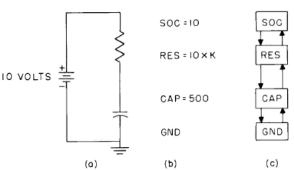
circuit and its typed representation (Fig. XV-1).
The battery will be called a "source" for this circuit and be represented by SOC. All voltages are taken with reference to ground, represented by GND.
(XV. CIRCUIT THEORY AND DESIGN) SOCO = 10 SOC RES=IOxK RES 10 VOLTS -CAP500 CAP GND GND (O) (b) (C)
Fig. XV-1. RC network: (a) circuit diagram; (b) typed representation; (c) flow chart.
SOC and GND. Basic elements must include the following equations for their current -controlled voltages:
Resistor: V = 104I
r
=-12
Capacitor: Vc Vs (between iterations, Vc + (T/500X10 ) I V
The time-interval variable T will be set at 1 pLsec so that the capacitor voltage change between intervals is given by
V + 2 X 10³ I-V
s s
In operation the source, SOC, starts activity by choosing a test current and sending it down to the basic elements. The control passes down the left path as shown in Fig. XV-1c, and is passed along by the basic elements. When control reaches GND, a voltage equal to zero is sent up the right side. This is the only function of GND - to reverse the direction of control and supply a voltage reference. Each basic element then adds its own voltage, as specified by the current, and sends the total voltage on to the next element. In this way, SOC receives a voltage for each current it sends out,
and its problem is to find a current that will return a voltage of 10 volts. a. Source
In the simple example of the RC network, the source decides which currents to try. As we shall see, the connections of a circuit must also originate test cur-rents and try to balance voltages. The method that was used in the program to select test currents, although not very elaborate, worked fairly well and ran with sufficient speed for the small circuits tested. This method was to calculate the intercept in the I-V plane of the source voltage with the straight line connecting the last two trial current-voltage pairs. If the last trial current was I, and the voltage that came back was V, and the current and voltage before that were I' and V', then the new trial current, It, is defined as
V I =0+S
t R
where R = (V'-V)/(I'-I), S = I - V/R, and V is the source voltage.
If, at the end of any trial, the voltage returned by the circuit is not equal to the sup-ply voltage within a small error tolerance, the source calculates a new trial current by using the new voltage-current pair and tries again. There are three special cases:
1) when I' = I and V' € V, R is left unchanged; 2) when I' # I and V' = V, R = 10 ohms; and
3) when I' = I and V' = V, R is left unchanged and (1.1) S - S.
These special cases occur often and are very important. If one of the calculations fails because of division by zero, the program may iterate forever and keep getting the same result. In Case 1, the same current is tried but a new voltage returns. This situation arises on the first iteration of an interval after the energy-storage elements have been changed. By leaving R the same as it was and only changing the bias variable S, the correct solution can be obtained on the next trial. Case 2 indicates that the circuit looks like a voltage source; this case is taken care of by making R small but not zero, since the circuit should not look like a battery for all currents. Case 3 is a degenerate case in which the same current has been tried and the same voltage received as in the
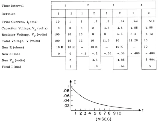
Time Interval Iteration Trial Current, Capacitor Volta Resistor Voltag Total Voltage, New R (ohms) New S (ma) New Vs (volts) Final I (ma) 1 2 3 4 1 2 1 2 1 2 1 2 It (ma) 10 1 1 .8 .8 .64 .64 .512 ge, Vs (volts) 0 0 2 2 3. 6 3. 6 4.88 4. 88 e, Vr (volts) 100 10 10 8 8 6.4 6.4 5. 12 V (volts) 100 10 12 10 11.6 10 11. 28 10 10 K 10 K - 10 K - 10 K - 10 0 0 -. 2 -. 2 -. 36 -. 36 -. 488 -. 488 2 3.6 4.88 5. 904 1 .8 .64 .5 .08 ,06 .04 .02 2 3 4 5 6 7 8 910 (M SEC)
(XV. CIRCUIT THEORY AND DESIGN)
previous trial. The best thing to do is change something and try again.
Now let us examine the first few iterations of the RC network in Fig. XV-1.
The
steps in a complete time interval are:
1) Compute It = V /R + S.
2)
Send I
tdown through elements to GND.
3) V = 0 at GND.
4) V
=
0 + V
sat CAP, where V
sis the old stored capacitor voltage.
5)
V = 0 + V + 10
s
4I at RES.
6)
Back at SOC.
Recompute R and S with I and V.
7)
Compare source and circuit voltages:
V 0
V
go back to 1).
V = V
go on to 8).
8) Change capacitor voltage, V + 2 X 10 I - V .
s s
9) Go back to 1).
With the values given and with Vs = 0, R
=
1000, and Is
=
0 at the start, the simulation
progresses as in Fig. XV-2.
The simulation of the simple RC network requires two iterations per time interval.
The first iteration is for the purpose of determining the new capacitor voltage; the
second, for checking the calculated current.
The actual currents calculated at
succes-sive time intervals follow a very simple difference equation.
I= (1-
) I
_or
I = 0.8 1
That is, the new current is 0. 8 of the last current. The actual decay during each
micro-second should be
-T/RC
I = (e
) I_
or
I = 0.818 I_
The error in the decay factor is due to the large steps that are taken. The approximation
-Xxe-x
=
1
-
x, which constitutes the first two terms of the series for e
,
is actually very
accurate for small x. Note, however, that the current follows a true exponential even
if the time constant is not exact.
b.
Connections
Thus far, we have only considered elements in series. When nodes appear in a
circuit they are restricted to three branches.
Several nodes may be used in series to
obtain more branches.
The three-branch node is called a connection or CON, M.
The
parameter M is the address of the third branch. Two other control elements must
be defined in conjunction with CON. These are STT, M and BAC, M. Their sole
pur-pose is to indicate that the control path should skip to the element at M instead of to the
RES= RI
VI-P CON,V3 V3- STT,VI
R CAP- Cl RES=R2 CAP RES
V2-- CON,V4 V4- BAC,V2 C CAP= C2 CON BAGI
T
C2 CAP (a) (b) (C)Fig. XV-3. A parallel RC network: (a) circuit diagram; (b) typed representation; (c) flow chart.
element above STT or below BAC. An example with connections is the parallel RC net-work shown in Fig. XV-3. The symbols Vl, V2, etc. in Fig. XV-3b are tags that indi-cate the address of the succeeding program element. The necessity for STT, BAC, and the tags should be apparent from Fig. XV-3c in which it is shown that the third control path from CON is sideways and must be turned up or down in order to connect with a basic element.
When CON receives a current down the right control path it does not pass it on as the basic elements do. It must calculate a probable split for the current between its two remaining branches. The procedure for determining the split is similar to that used by sources, complicated only by the fact that there are two branches. There is
also the possibility that a test current sent out along one branch may find its way around a loop to the other branch. This case is taken care of by making branch No. 2 look like a current source when branch No. 1 is being tested, and vice versa.
The basic formulas used by CON to split the incoming current I into two currents In and Im , when the past experience has produced the parameters R and S for branches
m and n, are: R I+R S -RS m nm nm n R +R n m I =I-I m n
The parameters Rk and Sk are computed as for a source, at every iteration based upon
the past two current-voltage pairs from the branch k. If the test currents In and Im do not produce identical voltages, then they are recomputed and tried again.
When a circuit contains connections, all of the elements must expect to have the control path travel up the left first and then down the right, as well as in the opposite
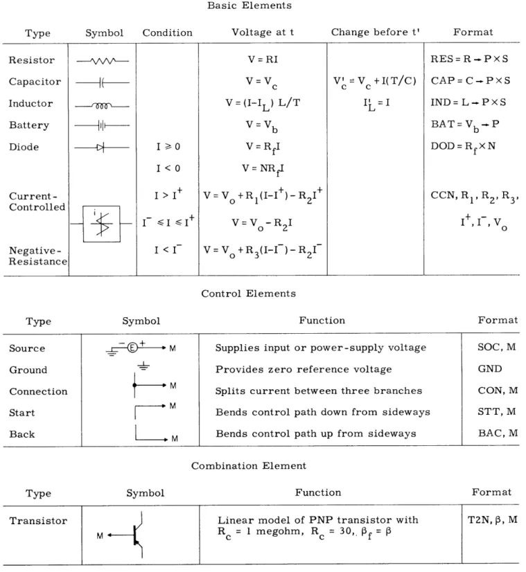
Table XV-1. Summary of element functions and format for use in the simulation program.
Basic Elements
Type Symbol Condition Voltage at t Change before t' Format
Resistor
-
V = RI RES = R - P X SCapacitor
V=V
V'V
+ I(T/C)
CAP=C - P x S
c c c
Inductor V = (I-IL) L/T I = I IND= L- P x S
Battery V = Vb BAT = Vb - P
Diode I > 0 V = RfI DOD = Rfx N
I<0 V= NRfI Current - I > I+ V = Vo + R1(I-)- R2 CCN, R1, R2' R3 Controlled I
<I
V=V -R I 1 V Negative- I < I V=V +R3(I-I )-R2 Resistance Control ElementsType Symbol Function Format
Source + M Supplies input or power-supply voltage SOC, M
Ground Provides zero reference voltage GND
Connection Splits current between three branches CON, M
Start M Bends control path down from sideways STT, M
Back M Bends control path up from sideways BAC, M
Combination Element
Type Symbol Function Format
Transistor Linear model of PNP transistor with T2N, 3, M
order previously considered. This is necessary because a connection sends out test currents in two directions, and with several such splits it is possible that test currents will be sent up or down any of the branches. The connections themselves must be capable of accepting an input current from any branch and splitting this between the remaining two branches. With all of the conditions necessary for a connection, the rules become too complex to state more explicitly.
A summary of the various elements that have been programmed thus far is given in Table XV-1.
3. Experiments
a. Flip-Flop Circuit Triggering
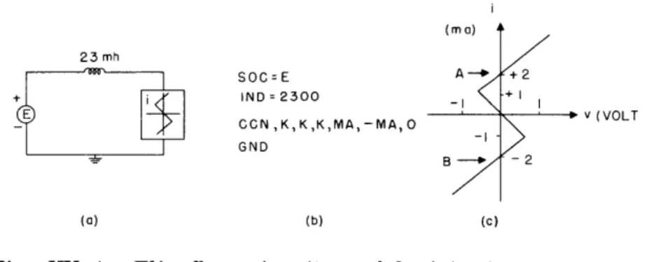
Analysis of a flip-flop reveals that it has a voltage-controlled negative resistance characteristic observed at the collectors of the two transistors. Therefore, rather than simulate the whole flip-flop, a negative resistance element was programmed and
simulated. The actual voltage-controlled element could have been programmed if a capacitance had been assumed in parallel, but in order to separate the stray capacitance from the flip-flop, a current-controlled element and an inductor were used. This is the dual of the flip-flop model and is just as useful. This model is shown in Fig. XV-4. (m a) 23 mh+2 IND = 2300 + I I E CCN,K,K,K,MA,-MA,O 2 V (VOLT -I GND (a) (b) (c)
Fig. XV-4. Flip-flop circuit model: (a) circuit diagram; (b) typed representation; (c) V-I characteristic.
The source that was actually used was the variable input waveform. This consisted of a pulse of variable width and amplitude, which was repeated at regular intervals. Because the circuit has two stable points, A and B in Fig. XV-4c, the pulse was made to alternate between positive and negative. Thus, if the pulse is sufficient to trigger the circuit, it will trigger it every time, otherwise the circuit will stay in one state.
The minimum pulse height necessary to trigger the circuit is a 1-volt pulse of infi-nite duration. Higher pulses require less time for triggering. Two basic pulse durations
(XV. CIRCUIT THEORY AND DESIGN)
(a) OPTIMUM-DURATION PULSE (b) MINIMUM-DURATION PULSE
(C) OPTIMUM-DURATION PULSE
Fig. XV-5.
(d) OPTIMUM-DURATION PULSE
Flip-flop circuit triggering. (a) Minimum pulse height, V
=
1 volt,
6 = 202 sec, VS = 202; (b) V = 2 volts, 6 = 30Fisec;
(c) V = 2 volts, 6 = 48 sec, VS = 96; (d) V = 4 volts, 6 = 23psec,
VS = 92.are important.
(See Fig. XV-5.) A pulse of minimum duration barely reverses the
cur-rent polarity. A pulse of optimum duration lasts precisely until the circuit reaches the
opposite stable state. With increasing pulse height the pulse area required for optimum
triggering approaches a limit
V = (Ia-I b ) L = 92 Lsec -volt
b.
RLC Oscillations
When an inductive element is added resulting series RLC network is capable
(a) SOC=0 RES=R IND = L CAP= C GND (b)
to the RC circuit shown in Fig. XV-1, the of oscillations. The iterative procedure, as in
Vr = IR
VI= (I-J) L/T J= I
V= S S= S1 +I_I(T/C)
Vr+V +Vc-o
Fig. XV-6.
RLC circuit: (a) circuit diagram; (b) typed representation;
(c) current-voltage equations.
the RC network, produces a current waveform that is the result of a difference equation. Without going through the complete iterative cycle, this difference equation can be derived from the equations for the elements. We shall assume that some energy has been stored at a previous time and consider the case in which there is a zero-voltage source. In this case, the iteration must satisfy the equations given in Fig. XV-6. The stored cur-rent J and stored voltage S are represented in terms of the previous curcur-rent I_1 and the previous stored voltage S_1. From these equations a difference equation for I can be developed.
(2LC
+ RCT
-
T 2L
LC + RCT I-1 RT + L-2
(i) For zero resistance: When R = 0 this difference equation should produce a non-decaying sine wave. If we set L = 1 and C = 1 so that the period is 2Tr, the interval T can be considered to be the radian measure between the sample points. The difference equation then becomes
I = (2-T 2
) I
-1 2It can be shown that this equation always produces perfect sine waveforms, except that the frequency will not be precise for large T. The true difference equation for sine waves is
I = (2 cos X) I_1 - _2
where k is the angle between samples. The approximation of 2 cos T by the first two terms of the cosine series, (2-T2), is very good when T is small.
(ii) For nonzero resistance: As R is increased from zero the multiplier on I_2 decreases from 1. This causes the sine wave to decay, as would be expected for a damped oscillator. With R negative and the multiplier greater than 1, the waveform increases in amplitude. All of these waveforms are very accurate when T is small.
The reason for the inaccuracy of the frequency and of the exponential time constant is that the capacitor and inductor have been approximated. But there is no instability,
such as can occur in some difference equations, and the error in normal operation is approximately one part in 106. Since 27-bit, floating-point arithmetic is used in the program, there is no problem with accuracy.
c. Limit-Cycle Oscillator
By substituting a current-controlled negative-resistance element for the resistor in the RLC circuit, the network oscillates so as to approach a limit cycle. Part of each cycle is spent using a negative resistance and part using a positive resistance. Thus,
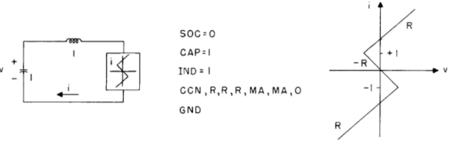
(XV. CIRCUIT THEORY AND DESIGN) R SOC=O I CAP=I +I V IND= I -CCN R,R,R,MA,MA,O -> GND R
Fig. XV-7. Limit-cycle oscillator: (a) circuit diagram; (b) typed representation; (c) V-I characteristic of negative-resistance element.
when the growth cancels out the decay, the limit cycle is reached. This type of oscilla-tion is typical of relaxaoscilla-tion oscillators and, with suitable parameters, can also
represent a sinusoidal oscillator.
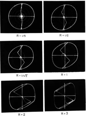
This type of network can best be studied by plotting current against capacitor voltage in the phase plane, Pictures of the nearly circular limit cycles were taken from the computer display. A symmetric negative-resistance element was used as illustrated in Fig. XV-7c.
The capacitor and inductor have been given the value 1 to normalize the units, since changing the resistance R is equivalent to changing L or C. With L and C equal to 1, R = 2 provides critical damping; R < 2, underdamping; R > 2, overdamping. Pictures were taken for several values of R with the negative resistance curve superimposed on the photographs. These photographs are shown in Fig. XV-8; in each picture the trajectory from the center to the limit cycle is included. In Fig. XV-9 the current waveforms are included to show the time dependence. In all of these photographs the values of L and C were not really 1 but were set at reasonable values to make the real value of R that was used vary around 2K. The dots in the waveforms are separated by
1-jisec time intervals.
4. Conclusion
Electronic circuit design can be speeded up considerably with the aid of a simulation program such as this one, if it is not too hard to use. The components can be changed, their values varied, and the critical waveforms can be viewed with an ease that could never be matched in a laboratory. A response occurring once can be run at any desirable speed and then locked on the display for study. Voltages and currents can be displayed in almost any conceivable manner and are automatically scaled. Time can even be run backwards if it is so desired. It becomes trivially simple to peak up a pulse just the right amount or adjust other parameters, such as the
P
of a transistor. Theoretical problems with ideal elements can be solved without worrying about lead capacitance or burning out elements.R = i/. "
R=2
R=I
R=3
Fig. XV-8.
Limit cycles with a symmetric negative-resistance element:
(a) relaxation oscillator, R
=
4; (b) R
=
1; (c) sinusoidal
oscillator, R = 1/4; (d) trajectory to limit cycle, R = 1/4.
(Normalized resistance R for L
=
1, C
=
1.)
(a)
(b)
(C) (d)
(XV. CIRCUIT THEORY AND DESIGN)
In spite of these advantages there are some drawbacks. Real elements are very hard to specify mathematically. Lead capacitance and inductance must be estimated and inserted as lumped elements. These factors make the analysis more or less ideal. Complex elements such as transformers and transistors must be specified in such detail as to make their use difficult. Until another program is completed, which will enable the drawing of a circuit on the computer display, the circuits are hard to put into the machine. Thus, unless a lot of work is to be done on one type of circuit it is not worth while to use an expensive computer. The main advantage in machine simulation is its use in conjunction with machine design. Here, full advantage can be taken of machine time because the input is a problem statement and the optimized, tested circuit is the
result.