Carbon Nanotube Field Effect Transistors for
Power Application
by
Tao Pan
Submitted to the Department of Electrical Engineering
and Computer Science
in partial fulfillment of the requirements for the degree of
Master of Science in Electrical and Computer Engineering
at the
MASSACHUSETTS INSTITUTE OF TECHNOLOGY
May 2007
@
Massachusetts Institute of Technology 2007.
All rights reserved.
Author ...
...
Department of Electrical Engineering and Computer Science
Mmr
16, 2007
Certified by ...
Anantha P. Chandrakasan
Joseph F. and Nancy P. Keithley Professor of Electrical Engineering
Thesis Supervisor
C ertified by ...
Jing Kong
Assistant Professor, Department of Electrical Engineering and
er Science
upervisor
Accepted by...
...
C. Smith
S INSTIT EChairman, Department Committee on Graduate Students
OLOGY2007
ZMARKER
MASSACHUS TT OFTECHL3G
i6
Carbon Nanotube Field Effect Transistors for Power
Application
by
Tao Pan
Submitted to the Department of Electrical Engineering and Computer Science
on May 16, 2007, in partial fulfillment of the
requirements for the degree of
Master of Science in Electrical and Computer Engineering
Abstract
Carbon nanotubes (CNTs) are nanometer-diameter cylinders formed from rolled-up graphene sheets which have found widespread interests due to their many excellent electrical properties. In particular, most of them are direct bandgap semiconductors from which carbon nanotube field effect transistors (CNTFETs) can be made. The small feature size and high electron mobility of the CNT makes it attractive and a good candidate to replace modern MOSFETs.
So far, most fabricated CNTFETs conduct currents only on the order of mi-croamps under low voltage bias which cannot be used to drive large output loads. In this work, we attempt to explore the ultimate performance benefits from
utiliz-ing multiple CNTs for CNTFETs. Two ways of makutiliz-ing multi-tube CNTFETs are
demonstrated in this thesis. Devices are fabricated, measured and analyzed. A sim-ple model is used to evaluate the ideal ballistic behavior of CNTFETs. Parasitics that are measured from experiments and extracted from numerical tools are added to the model. As an application, we compare the performance of CNTFETs with MOSFETs, both used as power transistors in a Buck DC-DC converter circuit.
Thesis Supervisor: Anantha P. Chandrakasan
Title: Joseph F. and Nancy P. Keithley Professor of Electrical Engineering Thesis Supervisor: Jing Kong
Title: Assistant Professor, Department of Electrical Engineering and Computer Sci-ence
Acknowledgments
I would like to thank my advisor, Anantha Chadrakasan for his trust to recruit me
and give me the opportunity to work on this project. Sharp, generous, supportive and always willing to listen to his students, Anantha has taught me a lot on doing research and showed me what makes a good advisor. There were many times that I am impressed by how Anantha remembers my needs even though he is the busiest person at MTL. I would like to thank my co-advisor Jing Kong. I thank her for her constant and warm support and encouragement. Thanks for her patience to help solving every trivia problems I encountered during my research and for her concern about my life.
I am lucky to be able work in Anantha's group. Each one of them has given me help. laughs, and friendships. I am grateful to Denis for giving me ideas and suggestions even before I came to MIT. Both Tim and Yogesh have given me a lot of feedback and comments on my work. And the work couldn't have been done without the answers from Joyce, Payam and Naveen about my endless questions on tools and softwares.I thank Manish, Vivienne, Jose, Alex and Alice for discussing about research and future. I thank Brian, Fred (both of them), Dave, Nathan, Daniel, Vikram, Ersin and Pat for many of the conversations and games that made life here fun and enlightening.
Having two advisors means doubling the number of friends. I thank Hootan for his constant critical questions and comments that led me to solve the problems. Without Mario's long nanotubes and passion to work, I may never have come up with this idea nor grown any tubes. I owe my thanks to Jae for his help in bonding the devices. And I thank Alfonso, Daniel and Stephen III for discussions on equipment usage and device fabrication.
Both carbon nanotubes and device fabrication are new fields to me. I really appreciate the discussions with Andy Fan, Cait Chleirigh, Xu Zhao, Andrw Ritenour, Hayden Taylor, Charles Hsu, Vicky Diadiuk at the early stage of my research that sped up my understanding of all the problems and issues.
This work couldn't have been done without the advices and knowledge from re-searchers inside and outside of MIT. I thank Tarek Moselhy from MIT's computational prototyping group for his patience to teach me using the capacitance extraction tool developed in his group. I thank Hongwei Gu from MIT Institute of Soldier Nan-otechnologies for providing me nanotube samples at the beginning. Prof. Wong from Stanford University is the world's leading researcher within the nanotube field. I appriciate him and his student Arash Hzeghi to let me have access to the code they developed. I also would like to thank Prof. Javey from University of California at Berkeley, Prof. Guo from University of Florida and David John and Dave Pulfrey from University of British Columbia to answer my questions through emails.
A lot of people have made the process of making nanotube devices enjoyable. I
feel lucky to know Kurt Broderick who is more like a friend than a staff, spending his non-office hours to help me fixing the machines and understanding the mechanism of the machines, although the latter is somewhat irrelevant to my work. I thank Mark Mondol for his dedication to his work. I also thank the advices and help from Pan Mao, JJ Hu and Eung Seok Park that saved me a lot trouble.
I am grateful for having friends on and off campus that is a solid part of my first two years in a new country. Stephen: Thank you for everything except for wasting my time. I will always cherish our shared experiences. Yuan: I always like your completely honest advices throughout the past 6 years. Sanquan: Thanks for listening to my complaints anytime. Greg, Gerrit, Dawei, Sagree, Tania, Jackie, Nicole, Sidney, Ranko, Hua and Sa: Thanks for being there.
Contents
1 Introduction 17
1.1 Motivation for Utilizing Carbon Nanotube Devices in IC Design . . . 17
1.2 Background on CNT Structure, Properties, and Synthesis . . . . 18
1.2.1 Carbon Nanotube Structure . . . . 18
1.2.2 Electrical Properties . . . . 19
1.2.3 Chemical Vapor Deposition (CVD) Synthesis . . . . 22
1.3 Thesis Contribution and Overview . . . . 23
2 Theory and Modeling of CNTFETs 25 2.1 CNT Electrostatics . . . . 26
2.2 Ballistic CNTFETs . . . . 27
2.3 Schottky Barrier Behaviors . . . . 28
2.3.1 Ohmic versus Schottky Barrier CNTFETs . . . . 28
2.3.2 Ambipolar Behavior . . . . 30
2.4 N-type and P-type CNTFETs . . . . 31
2.5 Gate Capacitance . . . . 32
2.5.1 Intrinsic Capacitance . . . . 32
2.5.2 Parasitic Capacitance . . . . 34
2.6 M ulti-tube Devices . . . . 37
2.6.1 CNT Network Devices . . . . 37
2.6.2 Devices with Parallel Aligned CNTs . . . . 38
3 CNTFET Device Structure and Fabrication Processes 3.1 Comparison of State-of-the-Art CNTFETs . . . .
3.2 Nanotube Film Devices . . . .
3.2.1 Nanotube growth . . . .
3.2.2 Device Fabrication . . . .
3.2.3 Selective Removal of Metallic Nanotubes . . . . .
3.3 Electrically Parallel Nanotube Array Devices . . . .
3.3.1 Nanotube growth . . . .
3.3.2 Device Fabrication . . . .
4 Measured Results
4.1 Nanotube Film Devices . . . . 4.1.1 DC Characteristics . . . .
4.1.2 Device Performance versus Device Geometry . 4.1.3 Selection of Semiconducting CNTs . . . . 4.2 Electrically Parallel Nanotube Array Devices . . . . . 4.2.1 DC Characteristics . . . .
4.2.2 Role of CNT Diameter . . . . 4.2.3 Role of CNTFET Geometry . . . .
5 Power CNTFETs in DC-DC Converter Circuit 5.1 Buck DC-DC Converter Circuit . . . .
5.2 Performance Benchmarking . . . . 5.3 Design Methodology . . . .
5.3.1 Optimizing the Number of CNTs . . . .
5.3.2 Optimizing CNT Diameter . . . .
5.3.3 Optimizing Spacing between CNTs . . . .
6 Conclusions and Guidelines for Future Work
6.1 Conclusions . . . .. . . . 6.2 Future W ork . . . . 43 44 47 47 48 51 53 53 55 61 . . . . 61 . . . . 61 . . . . 62 . . . . 63 . . . . 63 . . . . 64 . . . . 65 . . . . 66 67 67 70 71 72 72 73 75 75 76
A Analytical Expression for Ohmic Contact CNTFET Current 79
B Analytical Expression for CNTFET Gate Capacitance 81
List of Figures
1-1 Schematic models for grahene sheet and single-wall carbon nanotubes. (a) The chiral vector Ch = n&1 ± M&2 is defined on the 2D graphene sheet lattice [1]; (b) Three types of nanotube structures. Shown here is a (5,5) armchair nanotube(top), a (9,0) zigzag nanotube(middle) and a (10,5) chiral nanotube(bottom) [2]. . . . . 19
1-2 Energy dispersion relation of graphene . . . . 20
1-3 The wave vector k of CNT is shown in the Brillouin zone of graphene.
(a) metallic tubes n - m = 3q; (b) semiconducting tubes n - m = 3q. 20
1-4 One-dimensional energy dispersion relations for (a) armchair(5,5) nan-otubes; (b) zigzag(9,0) nannan-otubes; (c) zigzag(10,0) nanotubes. . . . . 21
2-1 (a) Schematic of a top-gate CNTFET; (b) Equivalent small signal cir-cuit model of the top-gate CNTFET. . . . . 26
2-2 Electrostatics of nanotube [3]. (a) Schematic diagrams of the potential profile along the channel; (b) Schematic of potential profile across the device. . . . . 26 2-3 I-V characteristics of an ideal Ohmic contact (19,0), DCNT=1.5nm
CNTFET. We assume 2nm thick TiO2 with its E = 40E, as gate di-electric. (a) ID versus
VGs;
(b) ID versus VDS. . . .. . . . .. . . . 292-4 (a) Ohmic contact CNTFET formation; (b) Schottky barrier CNTFET form ation. . . . . 30
2-5 The illustration of ambipolar behavior of CNTFETs. (a) Device is bi-ased on. Electrons pass through Schottky barrier; (b) Device is bibi-ased off. Large VDS gives electrons enough energy and narrows the potential barrier. Electrons still inject into the channel. . . . . 31 2-6 (a) Work functions of different metals and CNT; (b) ID-VGS of
fabri-cated devices with various contact metals [4] . . . . 32 2-7 Numerical simulation of CG,o, (a) Cross section of top-gate CNTFET;
(b) Discretizing metal electrode and CNT in 3D space; (c) Extracted
capacitance values of different discretizing granulation as compared to analytical value. . . . . 34
2-8 Gate capacitance dependence on device geometry. (a) CG,,, versus dielectric thickness; (b) CG,o versus nanotube diameter. . . . . 35 2-9 (a) Top-gate CNTFET with overlap capacitance; (b) Device cross
sec-tion presented in [5]; (c) Fringing capacitance in perfectly aligned device. 36 2-10 (a) Random network of nanotubes between source and drain; (b) Aligned
nanotubes between source and drain. . . . . 38
2-11 Current capacity degradation from CNT randomness. square: 1Im
by 1prm area.(a) Conductance versus channel length; (b) Conductance
efficiency versus channel length. . . . . 39
2-12 (a) The gate-to-nanotube capacitance versus pitch; (b) The unit width gate-to-nanotube capacitance versus pitch. . . . . 40
2-13 CNTFETs of vertically stacked CNTs. (a) parallel nanotubes; (b)
nanotubes stack on top of each other... 41 2-14 Electrostatics of different materials as channel. (a) metal; (b) silicon;
(c) C N T . . . . 41
3-1 Bottom-gate CNTFET structure. (a) Ref [6]; (b) Ref [7]. . . . . 45
3-2 Top-gate CNTFET structure. (a) Ref[5]; (b) Ref[8]; (c) Ref[9], [10]. 47
3-3 AFM image of densely grown nanotubes. . . . . 48 3-4 Fabrication step (1) - CNT growth. . . . . 49
3-5 Fabrication step (2) - source/drain contact deposition. . . . . 49
3-6 Fabrication step (3) - source/drain pads deposition. . . . . 49
3-7 Fabrication step (4) - 02 plasma etching of CNTs. . . . . 50
3-8 Fabrication step (5) -gate dielectric deposition. . . . . 50
3-9 Fabrication step (6) -gate electrode and pad deposition. . . . . 51
3-10 Photo mask of lcmx lcm die. . . . . 51
3-11 Electrical removal of metallic CNTs by applying high voltage pulses. . 52 3-12 SEM image of long straight nanotubes. . . . . 54
3-13 Measured diameter distribution by AFM. In Courtesy to Mario Hofmann 54 3-14 (a) Photo lithography step mask with various alignment markers; (b) Nanotube growth region and orientation. . . . . 56
3-15 CNT growth environment setup. . . . . 56
3-16 (a) A complete top gate CNTFET device pattern; (b) Zoom in of the source/drain cross digitized pattern with 1pm channel length, 10pm device width and 44 segments of CNTs in parallel; (c) Pattern to mea-sure CNTFET gate capacitance. . . . . 57
3-17 Photo mask and ebeam pattern of lcmx 1cm die. . . . . 59
4-1 (a) On resistance of 200pm wide devices with different channel lengths; (b) ION/IOFF ratio of 200pm wide devices with different channel length. 62 4-2 (a) Unit width conductance of devices with various W and L; (b) ION/IOFF ratio of devices with various W and L. . . . . 63
4-3 (a) ID-VGS curves before and after electrical burning; (b) ION/JOFF increases with tim e. . . . . 64
4-4 SEM images of fabricated CNTFETs. (a) Bottom-gate device with 100nm channel length and 200nm pitch; (b) A 1 am device and a 100nm device fabricated on the same CNT; (c) A top-gate device. . . . . 64
4-5 ID-VGS curves of two 44x W/L=10/1 CNTFETs fabricated on the same DCNT=1.45nm CNT with VDS ranges from
0.1V
to 1.5V. ... 655-1 (a) A Buck DC-DC converter topology; (b) PFM mode operation of the converter. . . . . 68 5-2 DC-DC converter block diagram concept with CNTFETs as power
transistors . . . . 69 5-3 Conversion efficiency of MOSFETs and CNTFETs. . . . . 71
5-4 Conversion efficiency versus CNT diameter. . . . . 73
B-1 (a) Cross section of CNTFET; (b) Infinite metal plate and hollow metal cylinder; (c) Mirrored metal cylinder; (d) Equivalent charged lines . . 81
List of Tables
2.1 Comparison of parasitic capacitance of different device structures. . 37
3.1 Comparison of key performances of state-of-the-art CNTFETs. . . . . 44 4.1 Role of CNT diameter on ION and IOFF .. . . . . . . . 66
4.2 Role of device channel length on ION and IOFF . . . . 66 C. 1 Fabrication process for electrically parallel CNTFET. . . . . 84
Chapter 1
Introduction
1.1
Motivation for Utilizing Carbon Nanotube
De-vices in IC Design
Aggressive scaling of CMOS devices over different technology generations has led to higher integration density and better performance. However, shrinking the conven-tional MOSFETs beyond the 45nm-techology node faces severe barriers due to the fundamental physics that constrains the conventional MOSFETs, such as exponen-tial increase in leakage current, large parameter variations caused by weak control of dopant atoms, quantum-mechanical tunneling of carriers through the thin gate oxide [11]. Hence, research has started in earnest to consider alternative devices and circuit architectures in the sub-50nm era. Among them, carbon nanotube field effect transistors are of particular interest.
Compared to MOSFETs, CNTFETs have several advantages. First, because of its one dimensional structure, near ballistic transport of carriers can be achieved which makes possible ultra fast and high efficient devices. Second, high-r dielectric materials can be used as gate dielectric without degrading carrier transport in the channel due to the absence of dangling bonds in carbon nanotubes. This leads to efficient gate field coupling that results in low subthreshold slope.
[7] [5] [9]. Simple logic gates (inverter, NOR, SRAM and ring oscillator) and analog
circuit (mixer) using CNTFETs have been demonstrated [12] [13] [14]. Although these circuits show potential and some of them operate at frequency as high as 50GHz
[13], a lot of challenges exist for nanotubes to fully replace CMOS technology. Thus,
a hybrid system where CNTFETs are selectively integrated into a CMOS chip is a plausible approach to demonstrate the advantage of nanotube devices and to improve circuit performance.
1.2
Background on CNT Structure, Properties, and
Synthesis
1.2.1
Carbon Nanotube Structure
Chirality
The structure of carbon nanotubes has been explored by high resolution TEM and STM techniques, yielding direct confirmation that the nanotubes are cylinders de-rived from the honeycomb lattice structure of the graphene sheet. Graphene sheet is shown in Figure 1-1(a). The structure of the nanotube is uniquely determined by its circumference vector Ch- ne1 + m&2 which connects two crystallographically
equiva-lent sites on a 2D graphene sheet. The cylinder connecting the two hemispherical caps of the carbon nanotube is formed by superimposing the two ends of the vector Ch.
In the (n, m) notation for Ch- nai l ma2 the vectors (n,0) or (0,m) denote zigzag
nanotubes and the vectors (n,n) denotes armchair nanotubes. All other vectors (n,m) correspond to chiral nanotubes. Figure 1-1(b) shows typical nanotube structures of different chiralities.
Single Wall and Multi Wall Carbon Nanotubes
When folding graphene layers into carbon cylinders, one can possibly get a single shell - single wall carbon nantubes (SWCNTs) or several shells - multi-wall carbon
(a) (b)
Figure 1-1: Schematic models for grahene sheet and single-wall carbon nanotubes. (a)
The chiral vector
Ch=
net+ ma
2is defined on the 2D graphene sheet lattice [1]; (b)
Three types of nanotube structures. Shown here is a (5,5) armchair nanotube(top),
a (9,0) zigzag nanotube(middle) and a (10,5) chiral nanotube(bottom) [2].
nanotubes (MWCNTs). MWCNTs consist of concentric CNT cylinders held within
each other by van der Waals forces. The distance between shells is approximately 3.4
A
,
which is close to the distance of two carbon layers in graphite.
The concentric shells of MWCNTs can differ in their chiralities and can
con-sist of both semiconduting and metallic nanotubes. If a MWCNT concon-sists of both
semiconduting and metallic cylinders, the metallic shells can negate the possible
semi-conducting properties. As a consequence, MWCNTs have a limited use as field effect
transistors. And thus for the rest of the work, we will be focusing on the SWCNTs.
1.2.2
Electrical Properties
Metallic and Semiconducting CNTs
Because carbon nanotubes are rolled up graphene sheet, in the circumferential
direc-tion periodic boundary condidirec-tions apply. The reciprocal space is obtained by doing
Fourier Transforms to the real space structure of CNTs. A periodical lattice structure
corresponds to a discrete energy dispersion relation, which can be viewed as sampling
the graphene E
-
k relation along the directions of certain wave vectors k. Figure
are the valence and conduction band respectively. At the K point, the valence and
conduction band intersects, resulting in a zero bandgap in graphene.
-5. -10
x 10 100-.. x 10
-2 2101
wave vector
Figure 1-2: Energy dispersion relation of graphene
Figure 1-3 shows how carbon nanotube's energy dispersion relation is obtained
from discretizing graphene's Brillouin zone.
K
K
K2 K2
K, K,
(a) (b)
Figure 1-3: The wave vector k of CNT is shown in the Brillouin zone of graphene.
(a) metallic tubes n - m = 3q; (b) semiconducting tubes n - m # 3q.
If the wave vector contains the K point (Figure 1-3(a)), there is no bandgap in the
nanotube band diagram, so that the tube is metallic. On the other hand, if the wave
vector doesn't contain the K point (Figure 1-3(b)), the conduction and valence bands don't intersect creating a gap between them and the nanotube shows semiconducting behavior. Theoretical analysis further reveals how chirality vector numbers n and m determine the conductivity of CNTs:
n-m = 3q metallic
n - m
$
3q semiconducting(1.1)
(1.2)
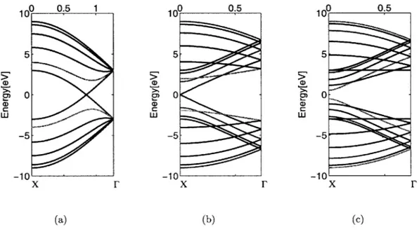
where q is an integer [15]. Therefore, all armchair (n, n) nanotubes are metallic. Only 1/3 of the possible zigzag (n, 0) nanotubes are metallic and 1/3 of the chiral nanotubes are metallic. Figure 1-4 plots the one dimensional energy dispersion relations for 3 different chiralities of nanotubes.
100.5 5-0 -5 -10. x C: LU IF (b) 100.5 5 0--5 -10
x
(c)Figure 1-4: One-dimensional energy dispersion relations for (a) armchair(5,5) nan-otubes; (b) zigzag(9,0) nannan-otubes; (c) zigzag(10,0) nanotubes.
For semiconducting tubes, the bandgap Eg is determined by
Eg = 0.8/d eV (1.3) 10 .5 5 0- -5--10 x ) U) 5. a) ) C LU r (a) F
where d is the diameter of the naotube and is again determined by the chirality vector,
d = V/5acc(m2
+
mn + n2)1/2/7- Ch/7r (1.4)where ac0 c is the CC bandlength in graphene. A typical single wall carbon nanotube
with a diameter of 1.7nm thus has a bandgap of around 0.47eV.
Electron Mobility Characteristics
Owing to their molecular uniformity and quasi-one-dimensional nature, nanotubes is expected to exhibit near ballistic transport properties. [16] and [17] report electron mobility in the range of 103 ~ 104cm2
/V-s
with the value derived from conduc-tance experiments in transistors. Theoretical prediction also yields a mobility of 10 4cm2/V.s in semiconducting tubes of radii up to ~2nm[18].
The current carrying capacity of multi-wall nanotubes has been demonstrated to be more than 109A/cm2
, without degradation (such as that due to electromigration) after several weeks well above room-temperature [19].
For CNTFETs, there're theoretical predictions that the normalized current density of a
1nm-diameter
single wall nanotube can reach the order of 108A/cm2 [1].1.2.3
Chemical Vapor Deposition (CVD) Synthesis
SWCNTs are difficult to grow. Currently, there are three methods to produce mass quantities of SWCNTs with a reasonably high yield, namely, arc discharge, laser ablation and CVD. Most of these processes take place at high temperatures. Large quantities of nanotubes can be synthesized by these methods. Advances in large scale and growth processes are making CNTs more commercially viable.
Among these methods, chemical vapor deposition shows most promise for indus-trial scale manufacturing in terms of low cost. It also has other advantages that it is capable of growing nanotubes directly on a desired substrate. The growth site is controllable by careful deposition of the catalyst. Also aligned nanotube growth has been made possible by controlling the direction of gas flow.
During a CVD, a substrate is prepared with a layer of metal (nickel, cobalt, iron) catalyst particles. This substrate is heated to approximately 900'C, with two gases - process gas (ammonia, nitrogen, hydrogen, etc) and carbon-containing gas (acetlylene, ethylene, ethanol, methane, etc) - to flow through the reactor to initiate the growth. the carbon-containing gas molecules decomposed at the surface of the catalyst particle, and the carbon dissolves. Once the solution becomes saturated, carbon will precipitate out in the form of CNTs. The detailed steps in this mechanism are still not well understood.
However, there're limitations with current CVD growth. For example, the chirality cannot be fully controlled by this process. Only a certain range and distribution of
CNT diameters can be achieved by changing catalyst size and gas flow.
1.3
Thesis Contribution and Overview
In this work, we are focusing on making CNTFETs with large current carrying ca-pacity that can be used in a hybrid CNT/CMOS system, in particular, a DC-DC converter circuit with the CNTFETs as power transistor switches. Chapter 2 focuses on the theoretical aspect of CNTFETs. First, we use a simple ballistic ID transistor model to describe the ultimate performance of CNTFETs. Then, both analytical and numerical calculations are presented when considering the parasitics in CNTFETs. A few device design guidelines and predictions are brought up based on this theoretical model. Chapter 3 first compared and assessed the most state-of-the-art CNTFETs and two different approaches of growing nanotubes and making CNT devices are de-scribed. In Chapter 4 measurements of the fabricated devices are presented. A few conclusions are drawn by discussing the relation between device performance and the design. The CNTFETs are put into a DC-DC converter circuit and benchmarked in Chapter 5. Finally, conclusions are drawn in Chapter 6 and a few suggestions for future work are proposed.
Chapter 2
Theory and Modeling of CNTFETs
There have been significant interest in predicting the ballistic transport and ultimate performance of CNTFETs and systems [20][21][22]. In this work, we are going to model a top-gate CNTFET with its schematic drawn in Figure 2-1(a) as the small signal equivalent circuit model in Figure 2-1(b).
The main function of the nanotube is modeled as a voltage controlled current source IDS that is determined by the gate-drain, gate-source voltages VGD and VGS. There are several capacitances to be considered. One is the intrinsic gate-to-drain and gate-to-source capacitance CGDi and CGSi. It consists of the quantum capacitance of the CNT and the capacitance between CNT and the gate electrode. CGDO and
CGSo are parasitic capacitances between the electrodes. They strongly depend on fabrication process and lithography quality. So far, overlap and fringe capacitance is one of the limiting factors of CNTFET application. We have ignored the capacitances between G/D/S electrodes and the substrate because CNTFETs are three terminal devices (MOSFETs are four terminal devices). Since bulk Si0 2 doesn't play a role in fabrication we could make it very thick. We need to consider this capacitance again if CNTFETs are integrated with Si process that they are fabricated on the same substrate. The contact resistance RD and RS are large in CNTFETs due to the fact that electrons have to travel from three dimensional metal bulk to one dimensional nanotube and also that it is challenging in fabrication to make good metal-CNT contact. The resistance caused by dimension difference is 6.5kQ [23].
CGDo CGDi RG
Gate
CG CGS CGSoL k-(a)Drain
.RD IDRs
Source
(b)Figure 2-1: (a) Schematic of a top-gate CNTFET; (b) Equivalent small signal circuit
model of the top-gate CNTFET.
2.1
CNT Electrostatics
IL I. x() (a) 0p qV, (b)Figure 2-2: Electrostatics of nanotube [3].
profile along the channel; (b) Schematic of
(a) Schematic diagrams of the potential
potential profile across the device.
As illustrated in Figure 2-2(a), the gate voltage applied at the device induces the
charges
Qint
in the nanotube channel. As a result, it shifts the Fermi level of the
nanotube pI due to the change of electron population in the subband. Thus
(2.1) VGS - VFB - A - Ao Qcnt
q CG,ox
where VFB is the flatband voltage and
po
the Fermi potential at the zero state(VGs=O).CGS?- CGDo
G
GSICGD
,CGBSi02
CDB Si Energy--CG,,, is the gate capacitance between the gate electrode and the nanotube.
Qct
can be calculated by neglecting charges due to holes and summing up electrons populated in the channel. It can be calculated as,fEi,max
Qcnt=
q
j31
D(E)(f
8(EI
p)
+
fd(E,1
-
qVDs))dE
(2.2)
D(E) is the ID universal nanotube density of states which can be calculated by first
principle [24]. For an ideal one dimensional device, carriers flow in both directions. Carriers propagating from source to drain are populated according to the source Fermi level while carriers going the opposite direction is populated according to the drain Fermi level. Figure 2-2(a) shows the Fermi level of the source and drain respectively.
2.2
Ballistic CNTFETs
To get a simple expression for drain current in CNTFET, we assume [3]:
* No Schottky barrier exists at contacts which means both source and drain elec-trodes can supply sufficient carriers to and sink carriers from the channel with-out reflection. This is true for Ohmic contact transistors. And it can be realized by using metals with the right work function.
D Backscattering or reflection due to the scatters or to the device structure in the
course from source to drain is neglected. Extensive studies show that under low bias, the mean free path(mfp) is observed to be - 1pm in CNTs and is thought
to be nearly elastic and limited by acoustic phonon scattering. Under high bias, optical emission dominates, and short (-10nm) mfp results
[25].
e The bandgap is sufficiently large so that the charge due to holes in the
va-lence band is neglected. By choosing CNT with certain diameters, this can be achieved.
Landauer-Biittiker equation [26] then gives,
ID
=
q E
[f(E, p)
-
f (E, p
-
qVDS)]dEj
(2.3)
where Ei is the energy of the ith subband, [ the Fermi potential, VDS the drain bias voltage and
1
f
(E, p)1 +
(2.4)1 + exp(
k)is the Fermi distribution function with Fermi level p and kB the Boltzmann constant. Integrating Equation 2.3, we get,
qkBT
I + exp[( P
- Em )/kBT] 1+ exp[(fp
- qVDS -E;-An)kBT
ID 7r n1+
x
In-E
i)/
rh 1+exp[ - Emin)/kBT] 1 + exp[(ii - qVDS - E7mn) /kBT] (2.5)
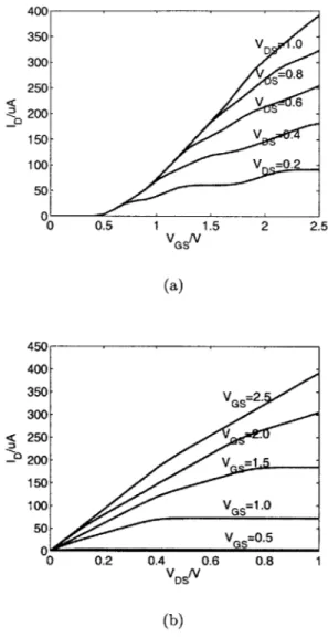
In order to calculate Equation 2.5, p must be obtained by solving Equation 2.1 in the previous section and the E-k dispersion relation can be obtained from discussions in Chapter ??. Figure 2-3 evaluates the I-V characteristics of a (19,0) CNTFET with a diameter of 1.5nm. High-rt dielectric is assumed in this device structure.
It shows in the plot that one CNT can have a channel resistance of as low as 2.5kQ plus 6.5kQ intrinsic resistance with 1.13fF/pm gate capacitance when a 2.5V gate voltage is applied. This is much smaller than its CMOS counterpart. Although this model doesn't describe some of the phenomenon observed in experiments, it does provide insight into the ultimate performance limit of CNTFETs.
2.3
Schottky Barrier Behaviors
2.3.1
Ohmic versus Schottky Barrier CNTFETs
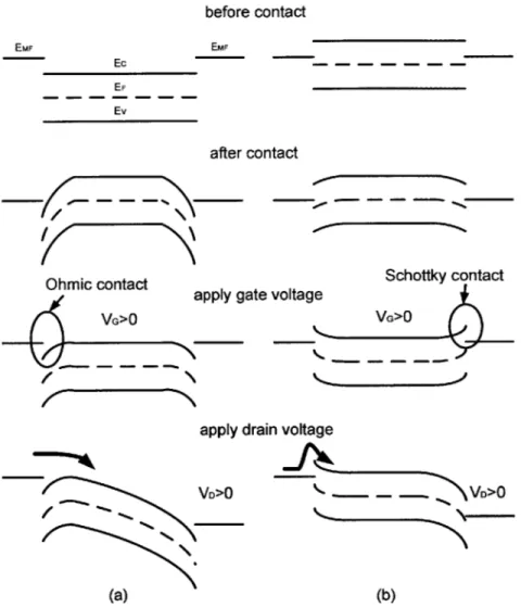
Experimental measurements suggest that most fabricated CNTFETs are not Ohmic contact but Schottky barrier CNTFETs. A Schottky barrier transistor is often caused by the formation of metal-semiconductor junctions. An illustration of different tran-sistor band diagrams is shown in Figure 2-4. Take an n-type trantran-sistor for example,
QUU - 350- 300- 250- 200-150. 100- 50-01 0 40U 400 350- 300-< 250 200 150 100-50 0 0 V .0 S=0.8 V -. 6 V V =0.2 0.5 1 1.5 2 2.5 VGSN (a) 0.2 0.4 0.6 0.8 1 V sN (b)
Figure 2-3: I-V characteristics of an ideal Ohmic contact (19,0), DCNT=1.5nm
CNT-FET. We assume 2nm thick TiO2 with its e = 40e, as gate dielectric. (a) ID versus
VGS;
(b)
ID
versus VDS.for Ohmic contact CNTFET, the Fermi level of contact metal is above the conduction band of the CNT which means both contacts are capable of providing infinite num-ber of electrons when the tube is conducting. When the two materials with different Fermi levels are connected, the Fermi potential automatically levels itself. Given a certain voltage applied at the gate, there is no barrier between the source and the channel so that electrons can pass through freely. On the other hand, electrons need to go through a barrier height of (Ec - EMF)/q in a Schottky CNTFET. The current
- VGS=2.
- V =1..
- VGS=1.0
before contact EMF EMF Ec EF Ev after contact
Ohmic contact apply g
VG>O
ate
Schottky contact voltage
VG>O
apply drain voltage
VD>O VD>O
(a) (b)
Figure 2-4: (a) Ohmic contact CNTFET formation; (b) Schottky barrier CNTFET formation.
is strongly dependent on the barrier height and width which are determined by the material characteristic and applied voltage.
2.3.2
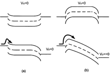
Ambipolar Behavior
Fabricated CNTFETs shows ambipolar behavior, i.e., transistors conduct current even when turned "further" off, especially if a large voltage(normally 4mV) is applied at its source and drain. There are two causes for this. First the CNT bandbap is usually small and CNT Fermi level lies in the middle of the bandgap. This means both electrons and holes have large probability to travel through the channel. Second
VG>O VG<O
VD>O
SVo>>O
(a) (b)
Figure 2-5: The illustration of ambipolar behavior of CNTFETs. (a) Device is biased on. Electrons pass through Schottky barrier; (b) Device is biased off. Large VDS gives electrons enough energy and narrows the potential barrier. Electrons still inject into the channel.
the Fermi level of the metal contact isn't near enough to either one of the conduction or the valence band. This phenomenon can be explained by Figure 2-4 and Figure
2-5. When the gate voltage is reversely biased, it creates a big hurdle for electrons,
yet it lowers the barrier for holes and causes a certain amount of holes to go through. Once a large VDS is applied, it narrows the barrier and provides the holes with enough energy. The OFF current is thus comparable to the ON current. This effect due to large VDS is more noticeable in short channel devices because voltage applied across the channel has stronger control over the electrostatics of the channel.
2.4
N-type and P-type CNTFETs
CNTs are assumed to have Fermi level lying in the middle of their bandgap so there is no distinction between n-type and p-type CNTs. The transistors show n-type and p-type behavior based on the different work functions of the contact metal. Theoret-ically, if the metal's Fermi level is near the CNT's conduction band, it is easier for electrons than holes to pass through and it is a n-CNTFET. Vice versa, if the metal Fermi level is near the valence band of the CNT, the FET is p-type. There is no real
measurement of the CNT work function. that of the graphene's work function. A contacts metals is shown in Figure 2-6(a).
2.9eV 3.6eV M MMg 4.1eV Al 4.4eV C E 4.8eV 5.1 eV
We use an estimation of 4.8eV [27] from comparison of work functions of possible
107
10-s
-40
5.6eV
(a)
Figure 2-6: (a) Work functions of different metals and devices with various contact metals [4].
-s (V 5 1
(b)
CNT; (b) ID-VGS of fabricated
The IV dependence on metal work function is demonstrated in experiments [4] where metals with large work function (Pd,Ti) form p-type devices and metal with small work function (Ca) forms n-type device. Devices with Mg contact (interme-diate work function) shows strongest ambipolar behavior. However, in experiment also, Ti (qm=4.4eV) and Cr (#m=4.4eV) still form p-type CNTFET. The reason is that the presence of absorbed oxygen affects the height of Schottky barriers at the surface, such that the Fermi energy is pinned closer to the valence band maximum, allowing tunneling of holes, but not electrons. Modeling of the Schottky CNTFETs is complicated. [28] and [1] are some good references.
2.5
Gate Capacitance
2.5.1
Intrinsic Capacitance
Looking at the gate capacitance, a nanotube is grown on a thick silicon dioxide and then surrounded by a thin gate oxide. A metallic gate rests on the thin oxide, creating a coaxial capacitance structure with the nanotube at the center. To get an analytical
IM9
equation of the capacitance between the gate and CNT we simplify the gate electrode to be an infinite plane and the CNT to be a metal cylinder. The capacitance between the two can be expressed as,
2ire
CG,ox = n
(2-6)
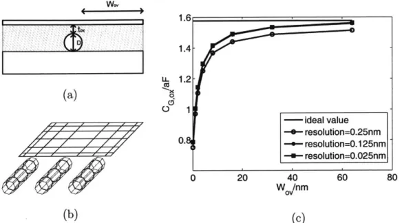
In reality, the gate is not infinite. We denote W, as the channel that is wider than the diameter of the CNT on both sides as illustrated in Fig.3-7(a). We use a multi-pole accelerated capacitance exaction software FASTCAP [29] developed at the Compu-tational Prototyping Group at MIT to numerically calculate the capacitance between gate and the nanotube. Figure 3-7(b) shows the discretization scheme. Figure 3-7(c) plots capacitance versus W. It shows that for the gate width that is exactly the same as the diameter of the nanotube (which is the most area-efficient case), the capacitance is only half of that calculated from Equation 2.6. The capacitance stays almost stable when W reaches about 60nm (30 times the dielectric thickness). This happens to be around the minimum alignment error that could be achieved today. Thus we consider the analytical solution as an accurate value in later device evalua-tions. The plot also shows that further increasing in W doesn't change the device performance except the fact the device size will increase. Using a coarse discretiza-tion (partidiscretiza-tion the cylinder in the circumferential direcdiscretiza-tion into eight), we reach an error of 4%. This error goes down to 1.1% when we discretize twice as much in all three dimensions. But it will be time consuming in complex simulations that involve multiple tube devices.
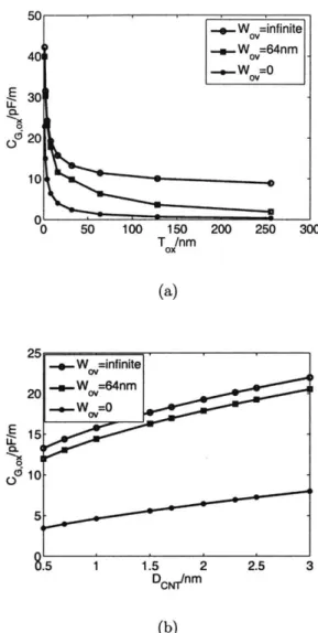
Figure 2-8 shows the gate capacitance dependence on different geometry param-eters of the FET structure. Here a channel length of 100nm is assumed. It can be seen that capacitance doesn't drop as drastically when dielectric thickness increases to above 100nm. This means an 100nm thick silicon dioxide basically has similar control of tube current as that of 250nm thick SiO2. It also shows that tubes with larger diameter couple with gate more. Bigger tubes intrinsically has smaller Schottky barrier for carriers thus are capable of conducting larger current. Stronger coupling
w." tox D 1.4-LL 1.2
-(a)
0 1 ideal value -4- resolution=0.25nm 0. -- resolution=0.125nm -- resolution=0.025nm 0 20 40 60 80 WO/nm(b)
(c)
Figure 2-7: Numerical simulation of CG,ox. (a) Cross section of top-gate CNTFET;
(b) Discretizing metal electrode and CNT in 3D space; (c) Extracted capacitance
values of different discretizing granulation as compared to analytical value.
with gate electrode further increases their conductivity.
In a bottom-gate structure, the capacitance is simulated slightly different since
the CNT is not surrounded by the same type of insulators anymore. Yet this turned
out not to be a big difference.
In a CNTFET, the gate capacitance is composed of two parts, C7 = C §j,'+C ,.
CG,ox is the electrostatic gate capacitance that we have just calculated. CG,q is the quantum capacitance of the nanotube. For simple calculations, the unit length single tube CG,q/L can be treated as 4 x 10--F/pim [30].
2.5.2
Parasitic Capacitance
Self-alignment is a revolutionary invention in the CMOS technology. It saves one step
of photolithography and reduces overlap capacitances between gate and source/drain significantly. Self-alignment in CNTFET is possible [5], but challenging. Therefore
most often there is overlap between gate and source/drain as illustrated in Figure 2-9(a), giving rise to parasitic capacitance. The state-of-the-art mis-alignment error using ebeam lithography is about 50nm. We will use this number for comparison
bL -.- WOV=infinite 40 -.-. W =64nm -.- W =0 30 2-20 20 10 0 50 100 150 200 250 300 T /nm Ox (a) 25 _..@WO=infinite 20 _**_WO,=_64nm 15 10. 5 5 1 1.5 2 2.5 3 DCN ,nm (b)
Figure 2-8: Gate capacitance dependence on device geometry. (a) CG,,, versus
di-electric thickness; (b)
CG,
0= versus nanotube diameter.
later.
The authors of [5] demonstrate a way to self-align top-gate CNTFETs. In theory
if materials can be deposited vertically, there won't be any overlap capacitance. In
reality, however, because of the slope of the profile as illustrated in Figure 2-9(b),
insulation of electrodes is realized by the natural oxidation layer of Al that is typically
4-8nm thick. Because this layer is thin and the dielectric constant of A1
20
3is higher
than SiO
2, this capacitance is considerable.
ca-GteD
(a)
T..
S D
(b)
Figure 2-9: (a) Top-gate CNTFET with overlap capacitance; (b) Device cross section presented in [5]; (c) Fringing capacitance in perfectly aligned device.
pacitance between gate and source/drain. Unlike MOSFETs, the S/D CNTFETs also serve as the source and drain contacts. This brings between these metal by a considerable amount. [31] gives an analytical
26W
Tgs/d + Tg +
un + (7Tg)2+2,stT r Ln + T,s/d _ u- Tg ,s/ d kEWn
7W
e Lun±Tg,.+
ln + S/id e IF n T, electrodes of the distance expression (2.7)for fringing capacitance of structure shown in Figure 2-9(c). Where ij = exp [(Led +
Lun-VLPu + Tg2 +2T,,dTg) /TrLd] and Tg,s/d = T. - Hda. k and r are constants and
[31] suggests values of 0.1 and 0.37 respectively. Lun in our case is 0.
Table 3.1 lists the parasitic capacitances of different device structures discussed above and compares them to the 32nm(Leh) CMOS technology predicted by Berkeley predictive technology model [32].
For a device with 70nm channel, this parasitic capacitance is about 3 times the intrinsic gate capacitance. And the ratio will increase with further scaled devices.
(c)
Q 11T
Device Parasitic Leh
TO
Eaiign Wsd TC/width
Fig2-9 (a) overlap - 8nm 50nm - - 430pF/pm
Fig2-9(b) overlap - 6nm 25nm - 50nm 660pF/pm
Fig2-9(c) fringing - 8nm - 200nm 50nm 108pF/pm
CMOS overlap 32nm 1.65nm - - - 170PF/pm
Table 2.1: Comparison of parasitic capacitance of different device structures.
2.6
Multi-tube Devices
2.6.1
CNT Network Devices
The maximum current capacity of one single SCNT is 25pzA [33]. In order to make a device that could conduct large amount of current, people have been trying to use multiple tubes. If hundreds of nanotubes could be put in parallel, they only occupy small areas and generate small capacitance.
However since making parallel aligned, dense CNT arrays is quite challenging, one alternative solution is to randomly put down nanotube network on substrate and deposit metal pads to obtain multi-tube devices. The schematic of this device is shown in Figure 2-10(a).
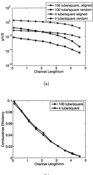
This method will reduce the current considerably. A MATLAB script is written to compare the random network device with the ideal case. We assume the nanotube lengths range between Inm and 5nm which is observed from AFM image. We choose a typical 50kQ as the resistance of one nanotube. The density of nantoube is determined
by the concentration of catalyst particles. We assume there is one catalyst particle in
every 0.1x0.l1m 2 and 0.5x0.5pm2 square which is also based on AFM images. The
channel length is varied from 100nm to 5pm in our comparison.
Figure 2-11(a) shows that only the curve of 100 tube/square, aligned nanotube has a conductance above IS and is better than a W=100nm transistor in 65nm technology node. The fact that the nanotubes are randomly distributed decreases
(a) (b)
Figure 2-10: (a) Random network of nanotubes between source and drain; (b) Aligned
nanotubes between source and drain.
the conductance for more than a factor of 10 even when the channel length is only
100nm. It goes down by another order of magnitude when the channel length reaches
5pm.
2.6.2
Devices with Parallel Aligned CNTs
Although carbon nanotubes in parallel with small pitches are still hard to fabricate,
it is useful for circuit designers to get the intuition of how the electrostatic will change
once multiple tubes are put together and screening effect begins to take place.
Again we use FASTCAP to perform the numerical calculation. We define "pitch"
as the spacing between two nanotubes(edge to edge). We also assume a 64nm
mis-alignment error in our structure as mentioned in Section 2.5 which is for fabrication
concerns. Figure 2-12(a) shows how gate capacitance depends on the pitches. As
the spacing between CNTs increases, the screening effect between them reduces and
there's more arc coupling with the gate so the capacitance increases more slowly. It is
interesting to note from Figure 2-12(b) that there is a maximum capacitance/width
value occurring at around 10nm for CNTs with 2nm diameter. This is different from
02--100 tube/square, aligned
1 ' ' -4-100 tube/square random
-u-4 tube/square aligned
00 -- 4 tube/square random 10" 0, 10-42 10 0 1 2 3 4 5 Channel Length/um (a) 0.1 -4-100 tube/square -u-4 tube/square >. 0.08 -.2 uL 0.06 0.04 0 o 0.02-0 1 2 3 4 5 Channel Length/nm (b)
Figure 2-11: Current capacity degradation from CNT randomness. square: 1pm by
1pm area.(a) Conductance versus channel length; (b) Conductance efficiency versus
channel length.
2.6.3
Devices with Vertically Stacked CNTs
Another question of interest is: Can we stack nanotubes on top of each other instead
of putting them in parallel as illustrated in Figure 2-13.
To answer this question, we need to understand that the nanotube is a discrete
material. For example, as we mentioned before, in order to increase current, we
increase the number of nanotubes under a shared metallic gate instead of increasing
the device width as is done for Si-based devices. In a CMOS device, when the gate
16 14 TO,/DCNT=4 12 10 To /DCNT=2 TJ/DCNT=1 6 4 20 10 20 30 40 50 60 CNT pitch/nm (a) 70 60-TO/D CNT-- 50-E L40 . T /DcN 30- T X/D -r 20-10 10 20 30 40 50 60 CNT pitch/nm (b)
Figure 2-12: (a) The gate-to-nanotube capacitance versus pitch; (b) The unit width
gate-to-nanotube capacitance versus pitch.
voltage increases, electrons from the substrate are attracted towards to the interface
with the dielectric material, forming a thin layer known as the inversion layer, as
shown in Figure 2-14(b). The number of electrons increases exponentially with the
gate voltage and the thickness of the inversion layer reaches a maximum value. That
may not happen in nanotubes. The electrical lines start from the gate and ends at
the source and drain which provide the mobile carriers. The nanotubes only serve as
channels being turned on and off between the source and drain. The difference of the
(a) (b)
Figure 2-13: CNTFETs of vertically stacked CNTs. (a) parallel nanotubes; (b)
nan-otubes stack on top of each other.
metal, silicon and stacked-nanotube device cross section is compared in Figure 2-14.
(a) (b)
Gate Metal Dielectric
Sour% ______ano_n _____ prain
(c)
Figure 2-14: Electrostatics
(c) CNT.
of different materials as channel. (a) metal; (b) silicon;
When there is a high carrier concentration at one end of the device, and one CNT
is incapable of transferring all of them to the other terminal, a second CNT will
conduct even though it's not under the direct control of the gate. Therefore, stacking
CNTs on top of each other might be an option to increase CNTFETs' current capacity
without increasing the device size.
Gate Metal Dielectric Metal Substrate Gate Metal Dielectric ~~~ ~~5 - U Q~~- ~~ Substrate Substrate -M
Chapter 3
CNTFET Device Structure and
Fabrication Processes
The first carbon nanotube field effect transistor using semiconducting CNTs was reported in [34] and [35] as early as in 1998. Ever since then, remarkable progress has been made to improve the performance of CNTFETs by approaches such as: reducing the gate oxide thickness, adopting high-rK dielectrics for the gate oxide, using electrolyte as the gate, reducing contact resistance by choosing proper contact metals and doing post processing treatments. These techniques have significantly improved the performances of CNTFETs that compare favorably to the state-of-the-art MOSFETs. In the first section of this chapter, we will compare and assess the state-of-the-art CNTFETs in literature.
One disadvantage with the reported devices is that since there's only one tube conducting, the on current is small. For power applications which require delivering
-100mA current, CNTFETs with multiple tubes need to be fabricated.
We are trying two approaches to fabricate CNTFETs with large current capacity. One way requires growing densely distributed nanotubes on chip and the devices are defined when metal contacts are deposited as source and drain at relatively arbitrary locations. The number of tubes connecting source and drain obeys statistics and are roughly proportional to the width of the device when the device is large enough. The maximum current is proportional to the number of tubes between two metal
contacts. A metallic nanotube removal process is required for this type of device and is the major challenge.
The second method involves growing one long straight nanotube and depositing a cross-digitized structure as source and drain to make use of many different seg-ments of the same long tube. This is equivalent to putting hundreds of nanotubes in parallel between source and drain. Although this method creates larger parasitic capacitances and resistances, this method overcomes the problem of low ION/JOFF ratio that is caused by the presence of metallic tubes. This method requires "high quality" nanonube growth. By 'high quality' we mean single-wall, long, straight, semiconducting single nanotube with a reasonable diameter. Fabrication process also needs to be carefully designed to locate a good segment of nanotube.
3.1
Comparison of State-of-the-Art CNTFETs
Table 3.1 lists the key performance and the-art CNTFET devices.
fabrication parameters of the most
state-of-Refs
[6]
[7]
[10]
[9]
[5]
[8]
Dielectric SiO2 SiO2 ZrO2 HfO2 HfO2 TiO2
Contact Metal Pd - - Pd Pd Pd Channel Length 600nm 18nm 3pm 2pm 50nm 1.24m Tube Diameter 1.8nm 1.lnm - 2.3nm 1.7nm 1.3nm Oxide Thickness 10nm 12nm 8nm 8nm 8nm 18nm ION/JOFF 105 106 103 103 103 104 RON/kQ 60 30 200 65 30 200
Table 3.1: Comparison of key performances of state-of-the-art CNTFETs.
[6] and [7] are two most recent back-gate (as illustrated in Figure 3-1) CNTFETs.
In [6], Pd contacts are used to minimize the Schottky barrier height for hole carriers at the metal/nanotube contacts. The nanotube is 1.8nm (calculated from distribution)
wide in diameter and the source and the drain are separated by 600nm. A very
thin layer of silicon dioxide (10nm) is used as bottom gate dielectric. Thin dielectric
is effective in controlling the current yet it is very prone to gate leakage because in
bottom-gate structure the gate area is much larger than that in the top-gate structure.
The fabricated device achieves IONIIOFF ratio > 105 under 0.5V bias and 55kg
turn-on resistance.
A common way to pattern source/drain contact is to use lithography (ebeam or
photo), deposit metal and do lift-off. [7] uses a different type of resist
hydrogensilse-quioxane(HSQ) to achieve ultra short (18nm) channel length. This work also uses
Pd as contact metal and grows nanotube of diameter as small as 1.1nm in order
to increase the CNT bandgap and thus to increase ION/IOFF ratio. The reported
ION/IOFF
ratio is 5.5x 10' at 0.4V bias and the ON resistance is 40ko. This work
adopts very thin(12nm) back gate dielectric layer as well.
Pd
CNT
Pd
Source
Drain
p-Si (back gate)
(a) (b)
Figure 3-1: Bottom-gate CNTFET structure. (a) Ref [6]; (b) Ref [7].
Recent top-gate CNTFET structures are shown in Figure 3-2. In 2002, Javey
et al. [10] for the first time used high-K insulator zirconium oxide (K ~25) thin
film (~8nm) as gate dielectrics by atomic-layer deposition (ALD). High-K material
afford high capacitance without relying on ultra-thin film thickness, thus allowing
for efficient charge injection into transistor channels and meanwhile reducing direct
tunneling leakage currents. With a
-3pm spacing between source and drain, this
device achieves more than
103 ION/IOFFratio even under 1V bias and 10' under
0.1V. The ON resistance is 200kQ. Later in 2003, Javey et al. [9] improved the same
type of device by changing the high-K. material into HfO
2and the metal contact into
103 under 0.3V bias voltage and an ON resistance of 65kQ.
A novel self-aligning technique was proposed by Javey et al. [5] again in 2004. In this work, 8nm HfO2 and 50nm Al gate electrodes were first deposited by ALD on top of SWCNT. This step takes advantage of native A1203 on the Al metal gate.
Very thin Pd metal (-7nm) is then deposited in the region and is separated by the HfO2/Al/Al 203 stack, forming the S and D electrode. The device structure is shown
in Figure 3-2(a). By this means, no high quality alignment is required. However, as we calculated in Chapter 2 the parasitic capacitance related to this structure is no smaller than a CNTFET without self-aligning. Also naturally formed oxide are not reliable to prevent leakage, which limits this method being used in mass production. The performance of this device, however, is the highest reported so far. It achieves
ION/1QFF ratio of 103 under 0.3V bias and an on resistance is 30kQ.
The latest work is done by Yang et al. [8]. The device employs Pd as electrodes for Ohmic contact and high-rc material TiO2 as gate dielectric. Device channel length
is 1.2pm. The interesting feature of this device is that the gate structure doesn't cover the whole channel, as shown in Figure 3-2(b). This means gate control over exposed nanotube is relatively weak. This device offers ION/IOFF ratio of 104 under 0.2V bias and the ON resistance of 200kQ.
Since these devices are fabricated with different processes and conditions, it is hard to compare because a lot of uncertainties exist. Yet it can be concluded that in order to get good performance, metal with high work function is very preferred. All devices use Pd as contacts. It seems CNT with small diameter gives better trade-off between conductance and JON/JOFF ratio, though theoretically, larger nanotube would be more conductive. This is probably because parasitic resistance overwhelms the influence of the tube diameter. For the same reason, device channel length does not make a big difference either. This leads us to try to use devices with longer channel to reduce the fabrication cost while maintaining the performance.
T102, Dielectric
(a) (b)
(c)