HAL Id: tel-02064277
https://hal.archives-ouvertes.fr/tel-02064277
Submitted on 11 Mar 2019HAL is a multi-disciplinary open access archive for the deposit and dissemination of sci-entific research documents, whether they are pub-lished or not. The documents may come from teaching and research institutions in France or abroad, or from public or private research centers.
L’archive ouverte pluridisciplinaire HAL, est destinée au dépôt et à la diffusion de documents scientifiques de niveau recherche, publiés ou non, émanant des établissements d’enseignement et de recherche français ou étrangers, des laboratoires publics ou privés.
In Situ Synchrotron X-ray Scattering of SiGe NWs :
Growth, Strain and Bending
Tao Zhou
To cite this version:
Tao Zhou. In Situ Synchrotron X-ray Scattering of SiGe NWs : Growth, Strain and Bending. Chemical Physics [physics.chem-ph]. Université Grenoble Alpes, 2015. English. �tel-02064277�
THÈSE
Pour obtenir le grade de
DOCTEUR DE L’UNIVERSITÉ GRENOBLE ALPES
Spécialité : PhysiqueArrêté ministériel : 3 Novembre 2014
Présentée par
Tao ZHOU
Thèse dirigée par Gilles RENAUD
préparée au sein du CEA-Grenoble/INAC/SP2M/NRS dans l'École Doctorale de Physique de Grenoble
In Situ Synchrotron X-ray
Scattering of SiGe NWs :
Growth, Strain and Bending
Thèse soutenue publiquement le 7 Décembre 2015, devant le jury composé de :
M. Daniel Bouchier
Directeur de recherche, IEF Orsay, Président
M. Pierre Müller
Professeur, Université Aix Marseille, Rapporteur
M. Yves Garreau
Professeur, Université Paris-Diderot, LMPQ, Rapporteur
M. Vincent Favre Nicolin
Docteur, CEA-Grenoble, SP2M, Examinateur
M. Tobias Schülli
Docteur, Responsable de la ligne ID01, ESRF, Examinateur
M. Roberto Felici
Docteur, Responsable de la ligne ID03, ESRF, Invité
SPIN-CNR, Roma, c/o Department DICII, University of Tor Vergata
M. Gilles Renaud
INTRODUCTION
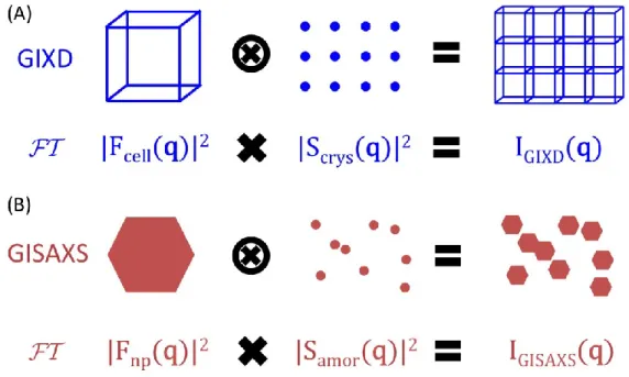
Nanoscale one-dimensional materials have stimulated great interest in the past decade thanks to their unique physical, electrical, optical and mechanical properties relative to their bulk counterparts. Among them, Si nanowires (NWs) are of particular interest due to their (1) being formed by the second most abundant element on Earth (2) high stability and non-toxicity (3) mature synthesis techniques and (4) direct compatibility with the booming microelectronics industry. Typically, Si NWs are grown with Chemical Vapor Deposition (CVD) via the Vapor-Liquid-Solid (VLS) mechanism, during which the NWs gradually emerge from the substrate as a result of preferential decompositions of the precursor gas on the liquid catalyst alloy droplets. Although discovered more than half a century ago (1964, R. S. Wagner and W. C. Ellis), many aspects of the VLS growth are still not well understood, since most experimental information was extracted from ex situ investigations, i.e. only when the growth process was terminated and after the sample was removed from its initial environment. In situ electron microscopy (EM) is, up to now, the major technique employed in both the qualitative and the quantitative studies of the growth mechanics. However, it usually requires laborious sample preparations and has a field of view that is limited to only a small area of the sample surface. Grazing Incidence Small Angle X-ray Scattering (GISAXS) and Grazing Incidence X-ray Diffraction (GIXD) complement the existing literature as they provide statistically averaged information on a much larger scale (~mm2). GISAXS reveals morphological information (size, spacing, faceting of the NWs)
similar to EM while GIXD offers, in addition, an unparalleled view of the structural properties such as strain, stress and atomic composition. To our knowledge, no in situ X-ray studies have been reported for the growth of SiGe NWs, mainly due to the difficulties
on the BM32 beamline at the European Synchrotron Radiation Facility (ESRF). Additional efforts have been made to further exploit the upgraded equipment to study the physical and mechanical properties of SiGe NWs.
This manuscript mainly centers on our current state of NW growth as well as our results on three different subjects, namely, the in situ growth of Si and Ge NWs, the strain evolution in Si-Ge core-shell NWs and the in situ bending of Si NWs. In fact, if it wasn’t too unorthodox a choice, I would give each chapter a very different title, which coincidentally (or not) reflects my path as an ordinary Ph.D. student.
Chapter 1 - Motivate. X-ray and nanowires are the two key components in this thesis work, but I have to admit that my motivation lies mainly in the former. I love everything about X-ray, which is why in addition to the basics of the several techniques essential to this work, a brief introduction to the history and characteristics of (synchrotron) X-rays is also included in this chapter.
Chapter 2 - Struggle. Chapter 2 is actually a literature review on the growth and characterization of Si and Ge nanowires. Instead of citing directly the results from other groups, I chose to present each time some ex situ Scanning Electron Microscopy (SEM) images on the NWs grown with our setup, followed by established explanations in the literature with regard to our observations. As a matter of fact, we struggled for a long time to find the optimal growth conditions appropriate to our new setup, only to reproduce what was very well understood in the literature.
Chapter 3 - Apply. The objective of this study is to apply our own expertise (X-ray techniques) to the problem. Despite knowing that most of the experimental aspects have already been covered by Electron Microscopy studies, we have performed a
comprehensive in situ follow-up on the simple NW growth, in hope of finding something that would complement the existing results (which we did eventually) and to demonstrate the viability of our techniques.
Chapter 4 - Excel. The next step is to further explore our specialties, to do what we excel at. X-ray is extremely sensitive to the changes in lattice parameters. This, combined with the knowledge of compound composition acquired with anomalous scattering techniques, allowed us to calculate the strain evolution during the formation and the annealing of the Si-core/Ge-shell heterostructure NWs.
Chapter 5 - Innovate. The final chapter is all about innovations. If we are not smart enough to invent a new X-ray technique, maybe we can find ourselves a unique problem to solve. It all started when we suddenly decided to stop rotating the sample when we were supposed to. Instead of growing a homogenous all-around Ge shell, atomic Ge was deposited on only one side of Si NWs, which led to the bending of the NWs. A new measuring technique (Stationary Method) was devised to follow in real time the bending process while the exact shape of the bent NWs was deduced by comparing the experimental data with results from an also original simulation. Finally, a theoretical model was built which allowed us to quantify the amount of misfit stress and surface stress that contributed to the bending.
ACKNOWLEDGEMENTS
Immeasurable appreciation and deepest gratitude for the help and support are extended to the following people who in one way or another have contributed to making this study possible.
My highest, most respectful gratitude goes to my mentor Dr. Gilles Renaud, Head of the BM32 beamline at the ESRF who, by kindly accepting me as an intern years ago, introduced me to the vast world of synchrotron radiation. Positive and enthusiastic even at the toughest times, Gilles is a quick-witted and knowledgeable person from whom there is always much to learn.
It is a genuine pleasure to express my deep sense of thanks and gratitude to Dr. Odile Robach for her keen interest in every stage of my research, for the most inspiring discussions and timely suggestions. I am also extremely thankful to my fellow colleague Dr. Fabien Jean for the exchange of ideas both inside and outside work, as well as to Dr. Nils Blanc and Dr. Valentina Cantelli whose selfless contribution had made this project possible.
I owe a deep sense of gratitude (and apology) to Dr. Laurent Vila, a brilliant research scientist at the CEA, for his kindness, enthusiasm and dynamism during our collaboration, despite a fruitless result. I would also like to thank our collaborators Dr. Laetitia Vincent and Dr. Charles Renard from IEF Orsay, for the countless instructive discussions over the years.
None of the experimental work would have been completed without the technical assistance of Olivier Geaymond, Olivier Ulrich, Dr. Frederic Boudaa and Dr. Harald Muller. There are just as much, if not more, to learn from them than from the others. I am also hugely indebted to Dr. Christina Revenant whose early guidance and advice proved invaluable in saving me from mis-steps.
for taking the time to read the manuscript and to participate in the defense of this thesis. Finally, I would like to thank all the other people I have had the privilege of working with (or bothering) over the course of this study. Francois Rieutord, Jean-Sebastien Micha, Joel Eymery, Denis Buttard, Pascal Gentile from CEA-Grenoble, Maurizio De-Santis, Johann Coraux, Aude Bailly, Marie-Claire Saint-Lager, Stéphan Arnaud from Institut Neel, Helena Isern, Thomas Dufrane, Jakub Drnec, Stelian Pintea, Willem Onderwaater, and Francesco Carla from the ID03 beamline of the ESRF, Gilbert Chahine from the ID01 beamline of the ESRF, Alesssandro Coati from the SIXS beamline of Soleil, Dr. Marie-Ingrid Richard from IM2NP Marseille, Frederic Leroy and Georges Sitja from CINaM Marseille, Geoffroy Prevot from INSP Paris, Guillaume Saint-Girons from ECL Lyon and Sebastien Linas from ILM Lyon.
ABSTRACT
This work summarizes the progress made on the BM32 beamline at the ESRF over the past 4 years since the launch of the CVD project, which was aimed at studying the in situ growth of SiGe nanowires, using synchrotron X-ray scattering techniques.
Results on the growth of Si and Ge NWs are first presented. The NWs length, size, spacing, facet morphology and their tapering angle are determined in real time with X-ray techniques. Special attention was paid to the very early stage of growth where changes in the shape of the AuSi liquid droplet were clearly observed. We also found clues indicating the presence of a metastable AuGe phase at the catalyst-substrate interface, the formation of which may be crucial to the sub-eutectic growth of Ge NWs.
Strain relaxation in Si-Ge core-shell NWs is presented next. The composition and strain were determined in situ as a function of the Ge overgrowth amount and of the annealing time, using anomalous X-ray scattering techniques. Their dependence on the NW size and on the shell growth temperature was also studied.
Finally, results on the in situ bending of as-grown NWs are shown. The bending was induced by depositing a second material on one side of the NWs. The strain and stress were determined by a combination of Bragg peak tracking, intensity simulation plus fitting and classic elasticity calculations. The bending induced by Ge deposition at 220°C is found to be mainly driven by the misfit stress, which scales almost linearly with Ge film thickness. On the other hand, the bending induced by Ge deposition at RT is found to be mainly driven by the surface stress, which evolves gradually from tensile to compressive for larger Ge thickness. A new technique was also devised which makes it possible to follow qualitatively the bending process. The NWs were seen dancing back and forth with increasing amount of deposition as revealed by real time stationary measurements with a 2D detector.
TABLE OF CONTENTS
1. CHARACTERIZATION TECHNIQUES 1 1.1. EXPERIMENTAL SETUP 1 1.1.1. SYNCHROTRON RADIATION 1 1.1.2. BEAMLINE BM32 4 1.2. CHARACTERIZATION TECHNIQUES 10 1.2.1. WHY X-RAY? 10 1.2.2. WHY GRAZING INCIDENCE? 121.2.3. (GRAZING INCIDENCE)X-RAY DIFFRACTION 17
1.2.4. (GRAZING INCIDENCE)MULTIWAVELENGTH ANOMALOUS DIFFRACTION 24
1.2.5. (GRAZING INCIDENCE)SMALL ANGLE X-RAY SCATTERING 30
1.2.6. OTHER TECHNIQUES 37 2. UHV-CVD GROWTH OF SI/GE NWS 41 2.1. VLSGROWTH AND UHV-CVD 41 2.1.1. NANOWIRES IN A NUTSHELL 41 2.1.2. VLS AND VSS 43 2.1.3. METAL CATALYST 44 2.1.4. CVD,MBE AND UHV-CVDGROWN NWS 47 2.1.5. SIZE EFFECT 49 2.2. NWGROWTH AT BM32 51 2.2.1. SI NWS 51 2.2.2. GE NWS 57 2.2.3. GE/SI RADIAL NWHETEROSTRUCTURES 64 2.2.4. GE/SI AXIAL NWHETEROSTRUCTURES 65 2.2.5. SI/GE AXIAL NWHETEROSTRUCTURES 69 2.2.6. GROWTH WITH COLLOIDAL GOLD 70 2.2.7. GROWTH WITH PATTERNED SUBSTRATES 73 2.3. CONCLUSION 75 3. IN SITU GROWTH STUDY OF SI/GE NWS 83
3.1. EXPERIMENTAL SETUP 83 3.2. SI NWS 84 3.2.1. SI NWS AS SEEN BY GIXD 84 3.2.2. SI NWS AS SEEN BY GISAXS 98 3.2.3. DISCUSSION 107 3.3. GE NWS 108 3.3.1. GE NWS AS SEEN BY GIXD 108 3.3.2. GE NWS AS SEEN BY GISAXS 117 3.3.3. DISCUSSION 119
4.1.1. GENERAL IN SITU MEASUREMENTS 122 4.1.2. STRAIN ANALYSIS BY ANOMALOUS SCATTERING 131
4.1.3. EFFECT OF POST-GROWTH ANNEALING 134
4.1.4. EFFECT OF NWSIZE 138
4.1.5. EFFECT OF GE GROWTH TEMPERATURE 140
4.2. MBEGE ON SI NWS 141
4.3. DISCUSSION 144
5. IN SITU NANOWIRE BENDING 149
5.1. EXPERIMENTAL SETUP 151
5.2. GE ON SI NWS AT 220°C 152
5.2.1. STRAIN:PEAK SHIFT 152
5.2.2. CURVATURE:INTEGRATED INTENSITIES 159
5.2.3. STRESS:CURVATURE 161
5.3. GE ON SI NWS AT RT 164
5.3.1. THE STATIONARY METHOD 164
5.3.2. STRAIN AND STRESS 166
5.4. AU ON SI NWS AT RT 168
5.4.1. AU ON SI NWS AT RT 168
5.4.2. SIDEWALL CONFIGURATION 171
5.4.3. SIZE EFFECT 173
5.5. DISCUSSION 175
5.5.1.THE DISPLACED BRAGG METHOD 175
5.5.2.GE/SI NWS AT 220°C 176
5.5.3.GE/SI NWS AT RT 179
5.5.4.AU/SI NWS AT RT 179
6. CONCLUSION AND OUTLOOK 183
APPENDIX I. WORKING WITH 2D DETECTORS AND PYROD I-1 APPENDIX II. ON CLASSICAL BEAM THEORY II-1
APPENDIX III. SAMPLE PREPARATIONS III-1
CHARACTERIZATION TECHNIQUES 1
1. CHARACTERIZATION TECHNIQUES
X-rays have long established themself as an invaluable and irreplaceable tool for studying the structure of matter. Even since their discovery in 1895 by Wilhelm Conrad Röntgen, tremendous progress has been made, not only to improve the sources that produce X-rays, but also to develop new and more powerful techniques that exploit them. The former has led to the construction of synchrotrons all over the world to generate X-rays far more intense and versatile than those produced by conventional laboratory sources. The latter is better understood by looking at the numerous experimental endstations built around the synchrotrons, called beamlines. Each of them makes use of one or more ways by which X-rays interact with matter, scattering, absorption, refraction, magnetic interaction, etc. in fields as diverse as physics, chemistry, biology, geoscience and paleontology.
The first part of this chapter consists of a brief introduction to synchrotron radiation. It is followed by a detailed presentation of the BM32 beamline at the European Synchrotron Radiation Facility, where all the X-ray measurements concerned in this dissertation were carried out. As for the second part, each section is devoted to providing basic knowledge of one of the characterization techniques that were used over the course of this work.
1.1. Experimental Setup
1.1.1. SYNCHROTRON RADIATIONSignificant breakthrough was made in applications of X-rays soon after their discovery, especially in the field of medical analysis. Meanwhile, little improvement had been made to the source. The Coolidge tube, developed by William David Coolidge in 1912 as a successor to Röntgen’s cathode ray tube, remained the standard X-ray source
for many decades before being replaced by the so-called rotating anode generators in the 1960s which allow for better heat dissipation, and hence higher power. When electrons (or other charged particles) moving at relativistic speeds are forced by magnetic fields to follow curved trajectories, they emit electromagnetic radiation tangentially to their path, known as synchrotron radiation. Theoretical considerations of synchrotron radiation can be traced back to the end of the 19th century, when Alfred-Marie Liénard (1898) and Emil
Wiechert (1900) worked out independently the expression for the radiated power of a relativistic particle undergoing centripetal acceleration in a circular trajectory. Experimental (visual) confirmation, however, had to wait until 1947 when a bright arc of
light was observed, mostly unexpectedly, through an unshielded area at General
Electric’s 70 MeV facility. Initially viewed as an unwanted phenomenon since it is responsible for the major energy loss in high energy particle accelerators, synchrotron radiation (wavelength of peak radiation ~300Å at the time) soon established itself as a viable source for spectroscopy experiments in the ultraviolet.
The 1st generation of synchrotron radiation facilities operated parasitically on
existing accelerators designed for particle physics studies. Consequently, the output of the radiation was limited by the low energy and low (electron) beam current of the host experiments. Dedicated sources (2nd generation) were later built as a result of the surging
demand for synchrotron radiation for the research in physics and in biology, with some being transformed directly from 1st generation facilities by means of upgrade.
Brilliance= Photons/second
(mrad2)(mm2)(0.1%BW) ( 1-1 )
A key factor that determines the overall quality of an X-ray source is its brilliance, which is given by the number of photons emitted per second (flux) divided by
CHARACTERIZATION TECHNIQUES 3
the solid angle of the radiation cone (angular divergence), the size of the source beam (source area) and the relative energy bandwidth (spectral distribution).
Figure 1-1: (Left) the average brilliance of X-ray sources. (Right) schematic of a 3rd
generation synchrotron.
X-ray beams generated by a 2nd generation synchrotron are about a millions times
more brilliant than those generated by a rotating anode. In other words, an hour of experiment at a synchrotron will otherwise take one century to complete in the home laboratory! The 3rd generation synchrotrons further extended the gap by another factor of
million through the introduction of wigglers or undulators, collectively known as the insertion devices. An insertion device can be viewed as a periodic magnetic structure that forces the electron to emit radiation multiple times by undergoing oscillations. In the case of an undulator, the period of the magnets is chosen in a way that the radiation emitted by a given electron from one oscillation is in phase with those from the others. The resulted coherent condition is the main driver behind the high intrinsic brilliance and monochromaticity (with harmonics) of the undulator radiation. It was later theorized that
not only the radiation from a single electron is coherent, but that the radiation from different electrons can be rendered coherent as well, either by self-seeding or by Self Amplified Stimulated Emission (SASE). The instrument that emanates from these concepts is called a free electron laser (4th generation light source), which boasts a peak
brilliance so high that few samples can withstand one single shot before being vaporized by the laser pulse. Its latest addition, the European X-ray Free Electron Laser, to be commissioned in 2016, is expected to achieve a peak brilliance of around 5×1033, some
10 orders of magnitude higher than the peak brilliance delivered by a normal undulator, as our pursuit for a more brilliant and more coherent X-ray source continues.
1.1.2. BEAMLINE BM32
Situated in Grenoble France, the European Synchrotron Radiation Facility (ESRF) is the world’s third largest 3rd generation synchrotron. (Figure 1-1 right) The electrons,
produced by a cathode electron gun, are first accelerated by the linear accelerator (LINAC) until their energy reaches ~ 200 MeV (99.9997% speed of light). They are then injected into the booster ring to receive a second energy bump to up to 6 GeV (99.9999996% speed of light), at which point they are transferred to the storage ring for user experiments. The 844.4 meters long (circumference) circular storage ring is in fact a polygon consisting of 32 straight and 32 curved sections in alternating order. In each of the 32 straight sections is hosted a variety of devices such as the RF cavities to help the electrons regain the energy loss due to synchrotron radiation, the focusing magnets (quadrupoles, sextupoles, etc.), and of course the undulators which serve as the main source of X-ray at a 3rd generation synchrotron. The electrons exiting one straight section
are redirected into the next by a 0.85T (or 0.40T) bending magnet (curved section). Synchrotron radiation emitted during this process can also be harnessed. At the ESRF, the endstations that utilize bending magnet radiation are labeled BM, to be distinguished
CHARACTERIZATION TECHNIQUES 5
from those labeled ID which utilize radiation generated by insertion devices. In the following paragraphs, the general properties of bending magnet radiation as well as X-ray beam characteristics of the BM32 beamline shall be discussed.
Figure 1-2: Schematics of the spectral distribution of (A) bending magnet radiation compared to that of (B) undulator radiation. Schematics of radiation emitted by (C) a non-relativistic and (D) a relativistic charged particle moving in a circular trajectory of radius ρ.
The spectral distribution of the radiation from a bending magnet (Figure 1-2A) is distinctly different from that from an undulator (Figure 1-2B). The latter is quasi-monochromatic, with a typical bandwidth of ~1% and a tunable fundamental wavelength (energy) whereas the former is a continuous function which extends from the X-ray to far infrared. A key parameter of bending magnet radiation is the characteristic energy which divides the spectrum into two parts of equal (50% each) radiated power. It also marks the
approximate location of the energy (frequency) beyond which the spectrum starts to fall off rather quickly. The characteristic energy is a function of both the electron energy ℰ𝑒
and the field strength of the bending magnet B. At BM32, it is calculated to be 20.6 keV which makes the beamline ideal for researches in the field of condensed matter physics.
ℏ𝜔𝑐[keV] = 0.665ℇ𝑒2[GeV] ∙ 𝐵[T] = 0.665 × 6.042× 0.85 = 20.6 [keV] ( 1-2 )
To understand the angular collimation of synchrotron radiation, we first consider the case of a non-relativistic charged particle. Its emitted pattern (Figure 1-2C), known as cyclotron radiation, is similar to that of an oscillating dipole with its maximum intensity in the direction perpendicular to the centripetal acceleration. In the case of a relativistic particle, this pattern is compressed into a narrow cone, the instantaneous direction of which is tangential to the circulating orbit. As can be inferred from Figure 1-2D, the nominal angular divergence of the bending magnet radiation in the vertical plane is the natural opening angle of the cone, and is equal to the inverse of the Lorentz factor:
𝛾−1= 𝑚
𝑒𝑐2/ℰ𝑒 = 0.511[MeV]/6[GeV] ~ 0.08[milli-radian] ( 1-3 )
Where 𝑚𝑒 is the rest mass of an electron and ℰ𝑒 is the electron energy inside the
storage ring. The actual angular divergence decreases for increasing energies, and equals ~1.5 times the nominal value when working at ℏ𝜔 = ℏ𝜔𝑐. In the horizontal plane, the
angular divergence is much larger as the electron radiates continuously while circulating along its orbit.
In most cases the emitted radiation does not meet the requirements to be used directly, instead, it has to first go through a series of optical devices put together in the optics hutch. Although the number of devices and the principles they operate upon (reflection, diffraction, interference and absorption) may vary significantly between
CHARACTERIZATION TECHNIQUES 7
beamlines, their objective is the same, to prepare a well collimated, focused and (very often) monochromatic beam optimized for each experiment. To do so, the large fan of radiation is first collected through a pair of slits, positioned at the entrance of the optics hutch, 23.84m from the source of radiation (bending magnet). The horizontal slit is widely opened to 23.84mm (= 1mrad) to accept as many X-ray photons as possible while still maintaining a minimum level of collimation for grazing incidence experiments (incidence angle ~ 2mrad). Before considering the opening of the vertical slit, we need to first understand the role of the first mirror. The 1.1m long Ir coated single crystal Si mirror is actually a high energy cut-off filter which absorbs incoming photons above its critical angle (c.f. Chapter 1.2.2). For a given material, the product of X-ray photon energy ℏ𝜔 and the corresponding critical angle θc is almost constant (Figure 1-3C).
ℏ𝜔[keV] ∙ 𝜃𝑐[mrad] ~ 𝐶 ( 1-4 )
For Si, we have C ~ 32. If we now simply set the inclination angle of the first mirror to, for instance θ = 1.6 mrad, then only photons with energy lower than ℏ𝜔𝑙𝑖𝑚 =
20keV are allowed to pass through. This is crucial for experiments with a monochromatic beam of for example 11keV, as it will help filter out the higher harmonics (22keV, 33keV, etc.) for the double crystal monochromator. Ideally we would like to apply this filter to all incoming photons in the vertical plane, since this is the plane where the x-ray is best (naturally) collimated. This however requires the opening of the vertical slit to be no less than two times the natural opening angle, which equals 3.81mm (0.08mrad at 23.84m) under our previous assumption. Moreover, to fully accommodate the incoming beam (Figure 1-3B), the product of the usable length of the first mirror (L) and its inclination angle (θ) should also be larger than 3.81mm. At θ = 1.6 mrad, this requires the mirror to be at least 2.38m long which is both expensive and impractical. The conundrum
is solved by the Ir coating at the mirror surface that increases the product in equation ( 1-4 ) to C ~ 87. Consequently, for the same energy ℏ𝜔𝑙𝑖𝑚, the inclination angle of the
mirror can be set to 2.7 times larger which in turn implies that the length of the mirror can be made 2.7 times smaller (L = 1.1m at BM32)!
Figure 1-3: (A) Schematics of the optical devices in the optics hutch of BM32. (B) Schematic view in the vertical plane of the entrance slit and the first mirror. (C) Line plot of the product of the photon energy and the critical angle of Si and Ir for energies between 8keV and 20keV.
With the opening of both entrance slits in mind, we can now estimate the peak flux at the exit of the optics hutch for a monochromatic beam (energy dispersion = 0.1% BW) with the following equation:
CHARACTERIZATION TECHNIQUES 9
Photons
second∙(0.1%BW)=1.33 × 10¹³ ℰ𝑒2[GeV] 𝐼[A] (Θ𝑣∙ Θℎ)[mrad
2] 𝑥2 𝐾
2/32 (𝑥/2) ( 1-5 )
where I = 0.2A is electron current in the storage ring, Θ𝑣 = 0.08mrad Θℎ=1mrad
are the effective angular acceptance of the vertical and horizontal entrance slits respectively, 𝑥 = 𝜔/𝜔𝑐 and 𝐾2/3(𝑥/2) is the modified Bessel function of second kind. Assuming a uniform distribution of photon density in both directions, we obtain 1.11×10¹³ photons/sec/(0.1%BW) for ℏ𝜔 = ℏ𝜔
𝑐 = 20.6 keV. In practice, the majority of
the measurements in this work were carried out in the vicinity of E = 11 keV in order to exploit the Ge K edge (c.f. Chapter 1.2.4), in which case the peak flux is slightly reduced to 1.06×10¹³. The x-ray beam is subsequently rendered monochromatic by the Si(111)
double crystal monochromator which applies the Bragg’s law (c.f. Chapter 1.2.3) to pick out photons with the required wavelength. Considering a monochromator with an energy resolution of 1.5×10⁻⁴ (0.015%BW), the peak flux of the monochromatic beam is hence
6.9×10¹¹. The second crystal of the monochromator (mono 2) is also slightly curved in
order to focus the beam in the horizontal plane. The focusing in the vertical plane is achieved by the second mirror, which in addition positions the x-ray beam back in the horizontal plane (parallel to the Y direction, Figure 1-3A). The beam is focused in a way that an exact copy of the source image is recreated at the sample stage. There is no point in further reducing the beam size as it will inevitably increase the beam divergence (degraded collimation) as stated by Liouville’s theorem. The beam size at the sample stage is thus determined by the size of the electron beam in the storage ring, which is 183μm (horizontally) by 30μm (vertically) at the ESRF. In practice, the final size is always slightly larger, mainly because of thermal deformation of the optical devices, despite them being constantly cooled by water.
1.2. Characterization techniques
1.2.1. WHY X-RAY?The physics society acknowledges the importance of the discovery of X-rays by awarding Röntgen the first ever Nobel Prize for Physics. In 1914 Max von Laue, and just one year later Sir William Henry Bragg together with his son William Laurence Bragg each received a Nobel Prize for their pioneering work that gave birth to X-ray crystallography. To date, a total of 15 Nobel Prizes have been honored to discoveries made in the field of X-rays. One can’t help but wonder, what makes X-rays so special?
[Short Wavelength] It is no longer a mystery that X-rays, like any other electromagnetic radiation, exhibit both wave and particle properties at the same time (wave-particle duality). X-rays have a wavelength of around 1Å, making them ideal for resolving atomic and molecular structures which share a comparable characteristic length, either via diffraction (Bragg’s law) or via direct imaging (Rayleigh’s criterion).
[Ideal Energy] As a particle, an X-ray photon possesses a typical energy of 0.12-120 keV, which covers the binding energy of most elements, from C K edge (0.284keV) to U K edge (115.606keV). A photoelectric event takes place when an X-ray photon is absorbed by the material, ejecting a core electron in the process. The resulting absorption spectra (absorption coefficient versus photon energy) contain information on the local structure and electronic states of the subject, the analysis of which lies at the heart of most X-ray absorption spectroscopy techniques (e.g., EXAFS, XANES). Alternatively, the emitted photoelectron can be studied. This gives rise to a bunch of techniques collectively known as X-ray photoemission spectroscopy (e.g., XPS, ARPES), whose main focus is to resolve the electronic structure and chemical state of the given material.
[Strong Penetration] X-rays are known for their penetration ability, especially those with higher energies (12-120keV) otherwise known as hard X-rays. The advantages
CHARACTERIZATION TECHNIQUES 11
are twofold. First of all, high penetration means little requirement on sample thickness, as opposed to the delicate sample preparation for, for example Transmission Electron Microscopes. This is one of the two reasons (the other one being the short wavelength) behind the popularity of X-ray imaging techniques such as radiography and tomography. Secondly, high penetration also implies little interaction, which is why X-ray is generally considered as a non-destructive method for the study of solid state physiques.
[Tunable Polarization] Synchrotron sources naturally produce X-rays which are linearly polarized in the horizontal plane (viewed from within the orbital plane), with possibilities of introducing circular and elliptical polarizations at the optics stage. The high degree of polarization and versatile nature of synchrotron X-rays make them the perfect tool for the study of magnetic properties in the subject material.
Below is a list of some commonly used techniques that can be found on a synchrotron beamline, classified by the interaction of X-rays with matter on which the techniques are based.
Interaction Techniques Wavelength Short Energy Ideal Penetration Strong Polarization Tunable
Scattering
X-ray Diffraction ☐
Small Angle Scattering ☐
Resonant Scattering ☐
Coherent Diffraction Imaging ☐
Absorption
Absorption Spectroscopy ☐ ☐
X-ray Dichroism ☐
Emission Spectroscopy ☐
Absorption Contrast Imaging
Refraction Phase Contrast Imaging
Table 1-1: A list of some commonly used techniques that can be found on a synchrotron beamline. stands for if a property, e.g. short wavelength, is fundamental to the application of the technique. stands for not required ☐ stands for optional.
1.2.2. WHY GRAZING INCIDENCE?
Figure 1-4: (A) Schematics of the reflection and refraction of a plane wave propagating from an optically denser medium to a less dense one. (B) The refraction of the out-going wave using the reciprocity theorem. (C) The penetration depth (in log scale) in the case of Si for 11keV x-ray. (inset) the same plot with linear scale shows that the penetration depth tends to sin(𝛼𝑖) 𝜆/4𝜋𝛽 for large incident angles. (D) The effective scattering depth as a function of the exit angle for various values of incident angle. (E) The difference between the out-of-plane component of the momentum transfer in the vacuum and in the sample as a function of the exit angle for various values of incident angle. (F) Absolute square of the incoming transmittance as a function of the incident angle.
CHARACTERIZATION TECHNIQUES 13
(red solid lines, Figure 1-4A) When an electromagnetic wave travels from a medium with a larger refractive index n to one with a smaller index n’ at incident angle 𝛼𝑖, part of wave is reflected back at 𝛼𝑟 = 𝛼𝑖, the rest continues to propagate inside the
second medium following a slightly deviated trajectory. In terms of Snell’s law, this is written as
cos 𝛼𝑖 cos 𝛼𝑖′=
𝑛′
𝑛 ( 1-6 )
Since 𝑛 > 𝑛′, the refraction angle 𝛼𝑖′ is always smaller than the incident angle
𝛼𝑖. (blue dashed lines, Figure 1-4A) Intuitively if we start to reduce 𝛼𝑖, it will come to a
point 𝛼𝑖 = 𝛼𝑐 where 𝛼𝑖′ becomes 0. 𝛼
𝑐 is called the critical angle below which the
incident wave appears to be completely reflected. For visible lights, the phenomenon is known as total internal reflection, and is commonly observed when light is projected from a transparent material (water n=1.333, glass n=1.46) into vacuum (n=1) or air (n=1.000293). In the case of X-ray, a similar event occurs when the beam is impinged from vacuum (n=1) onto any surface at sub-critical angle, as all materials turn out to have a refractive index (slightly) smaller than unity. The phenomenon is called total external reflection with the term external referring to the fact that the reflection now takes place in the vacuum and thus outside of the given material. We shall ignore absorption at the current stage and present the expression of the refractive index n as follows
𝑛 = 1 − 𝛿 = 1 − 2.701 × 10⁻⁶(𝑍/𝐴) 𝜌[g/cm3]𝜆2[Å2] ( 1-7 )
Z is the atomic number (14 for Si), A is the atomic mass (28.085 for Si) and ρ is the mass density (2.329 for Si). Exchanging n with 1 and 𝛼𝑖′ with 0 in Equation ( 1-6 )
δ is extremely small, of the order of 10-6 or 10-5 (4.034×10⁻⁶ for Si at 11keV). This
allows the above equation to be further reduced to 𝛼𝑐 = √2𝛿, with typical value of 𝛼𝑐
of the order of several mrad (0.163° for Si at 11keV). In reality, besides being refracted, the x-ray is also being gradually attenuated whilst travelling in the material. The refractive index should thus be extended to a complex number to take into account the absorption process.
𝑛 = 1 − 𝛿 + 𝑖𝛽 ( 1-9 )
Since both 𝛼𝑖 and 𝛼𝑖′ are small, Equation ( 1-6 ) can be rewritten as
𝛼𝑖2 = 𝛼
𝑖′2+ 2𝛿 − 2𝑖𝛽 = 𝛼𝑖′2+ 𝛼𝑐2− 2𝑖𝛽 ( 1-10 )
β is also small and varies from 10-8 to 10-5, depending on the material (5.068×10⁻⁸
for Si at 11keV). Solving the above equation, we obtain 𝛼𝑖′= Re(𝛼 𝑖′) + 𝑖 Im(𝛼𝑖′) Re(𝛼𝑖′) = (√(𝛼𝑖2− 𝛼 𝑐2)2+ 4𝛽2+ (𝛼𝑖2− 𝛼𝑐2))1/2/√2 Im(𝛼𝑖′) = (√(𝛼𝑖2 − 𝛼 𝑐2)2+ 4𝛽2+ (𝛼𝑐2− 𝛼𝑖2))1/2/√2 ( 1-11 )
The classical description of the refracted wave writes (ignoring the electric field) exp (−𝑖𝑘𝑖′𝛼𝑖′𝑧) = exp(−𝑖𝑘𝑖′Re(𝛼𝑖′)𝑧) exp (𝑘
𝑖′Im(𝛼𝑖′)𝑧) (for 𝑍 < 0) ( 1-12 )
The second term describes an exponential decay of the wave amplitude as it propagates further into the material. For 𝛼𝑖 > 𝛼𝑐, Im(𝛼𝑖′) is small, and tends to
𝛽/ sin 𝛼𝑖, which is common for a linear absorption process (Figure 1-4C inset). For
𝛼𝑖 < 𝛼𝑐, the imaginary part becomes more prominent, resulting in a sharper dampening
of the wave amplitude. The direct implication is that the refracted wave, called evanescent, is now confined to just a few hundreds Angstroms below the surface (Figure
CHARACTERIZATION TECHNIQUES 15
1-4C). In other words, only the region close to the surface is probed by impinging x-rays at angles below the critical angle. The enhanced surface sensitivity is one of the two reasons as to why almost all x-ray surface science experiments are conducted under grazing incidence.
To quantitatively evaluate the surface sensitivity, we shall introduce the classic 1/𝑒 penetration depth, which is defined as the depth at which point the intensity falls to 1/𝑒 (or 1/2𝑒 when it comes to the amplitude) of its original value at the surface. From Equation ( 1-12 ), immediately we have
Λ𝑖 = 1
2𝑘𝑖′Im(𝛼 𝑖′)
( 1-13 ) For a complete scattering process, the contribution from the out-going wave (the one that is measured by the detector) should also be taken into consideration. The analysis is made simple by the use of the reciprocity theorem which allows us to proceed the analysis in a similar manner as we did with the incoming wave.
𝛼𝑓′ = Re(𝛼 𝑓′) + 𝑖 Im(𝛼𝑓′) Re(𝛼𝑓′) = (√(𝛼 𝑓2− 𝛼𝑐2) 2 + 4𝛽2+ (𝛼 𝑓2− 𝛼𝑐2))1/2/√2 Im(𝛼𝑓′) = (√(𝛼 𝑓2− 𝛼𝑐2) 2 + 4𝛽2+ (𝛼 𝑐2− 𝛼𝑓2))1/2/√2 Λ𝑓 = 1 2𝑘𝑓′Im(𝛼 𝑓′) ( 1-14 )
The effective scattering depth is given by 1 Λ= 1 Λ𝑖+ 1 Λ𝑓 ( 1-15 )
It can be inferred from the above equation that Λ is dominated by the smaller of the pair Λ𝑖, Λ𝑓, which is why the effective scattering depth is always small (i.e. always
incidence experiment. Figure 1-4D shows such dependence as a function of the exit angle for various values of incident angle. At 𝛼𝑖 = 𝛼𝑐/2 and at 11keV, X-rays merely
penetrate into 3.6nm of Si, which is equal to 11.5 monolayers along the [111] direction. Before moving on to the second advantage of grazing incidence experiments, let us take a last look at Equations ( 1-11 ) and ( 1-14 ). We have previously established that the imaginary part of the refraction angle is associated with the absorption process as the wave propagates inside the material. The real part is in fact useful for calculating the out-of-plane component of the momentum transfer qz’ (c.f. next section) inside the sample which, for reason of simplicity, is often replaced by its counterpart in vacuum qz.
𝑞𝑧′,sample= 𝑘(sin(Re(𝛼𝑖′) + sin(Re(𝛼𝑓′))
𝑞𝑧,vacuum = 𝑘(sin(𝛼𝑖)+sin(𝛼𝑓) ( 1-16 )
Figure 1-4E shows the offset between the two values as a function of exit angle for various incident angles. The offset is at its largest for 𝛼𝑖 = 𝛼𝑐. For a given 𝛼𝑖, the
offset is peaked at 𝛼𝑓= 𝛼𝑐 then gradually decreases with increasing exit angle. This
offset is the main reason why the same out-of-plane Bragg peak of the Si substrate (with refraction) is separated from that of the Si nanowires (without refraction) in a case presented in chapter 5, and should be corrected for most quantitative analysis.
When the incident wave arrives at the surface, its power is distributed between the reflected wave and the refracted (or evanescent) wave. The fraction of the incident power that goes to each part is given by the reflectance R and transmittance Ti, respectively, and can be calculated with Fresnel’s equations
R =𝛼𝑖− 𝛼𝑖
′
𝛼𝑖+ 𝛼𝑖′ , 𝑇𝑖 =
2𝛼𝑖
𝛼𝑖 + 𝛼𝑖′ ( 1-17 )
R + 𝑇𝑖 = 1, as is dictated by the conservation of energy. Let us first ignore
CHARACTERIZATION TECHNIQUES 17
becomes 0 and hence |𝑅| = 1. This indicates that all incoming x-rays are reflected back from the surface, which coincides with our previous conclusion of total external reflection below the critical angle. At 𝛼𝑖 = 𝛼𝑐, we have 𝛼𝑖′= 0 and as a result 𝑇
𝑖 = 2.
This is an intriguing feature as it implies a two-fold increase in the evanescent amplitude and a four-fold increase in the evanescent intensity! The enhanced signal at critical angle is the second reason for working under grazing incidence. Figure 1-4F shows |𝑇𝑖|2 as a
function of the 𝛼𝑖, with and without taking absorption into account. Note that the overall
intensity of the scattering process is at the same time affected by the transmittance of the outgoing wave, which also amounts to 4 for 𝛼𝑓 = 𝛼𝑐. However, one can rarely benefit
from the enhanced |𝑇𝑓|2 since 𝛼𝑓 is seldom fixed in surface diffraction experiments.
1.2.3. (GRAZING INCIDENCE)X-RAY DIFFRACTION
Figure 1-5: Schematics of an incoming wave with wave vector ki scattered by an electron
at re and definition of the real space vectors used in equations ( 1-18 ) to ( 1-26 ).
Before we dwell on the classical interpretation (as opposed to derivation with quantum mechanics) of X-ray diffraction by crystalline materials, we need to first introduce the three conditions that help reduce significantly the complexity of the problem, namely, elastic scattering, the Fraunhofer limit, and kinematical approximation. (Figure 1-5) Let us neglect polarization and consider simply an incident wave with amplitude E0, being scattered by an electron at re. The outgoing wave is viewed by an
observer (detector) placed at a distance R0 from the scattering center. The Fraunhofer
limit, also called the far-field limit, requires that the distance R0 to be sufficiently large. This allows us to treat both the incoming and outgoing X-rays as plane waves, with their amplitude being related by
𝐸1exp(−𝑖𝐤𝐟∙ 𝐫𝐞) = 𝐸0
𝑟0
𝑅0exp(−𝑖𝐤𝐢∙ 𝐫𝐞) ( 1-18 )
where 𝑟0 = 𝑒2⁄𝑚𝑐2 = 2.82 × 10⁻¹⁵m is the classical radius of electron, also
known as the Thomson scattering length. ki and kf are the wave vectors for the incoming
and outgoing wave, respectively. Thomson scattering is essentially elastic (to be distinguished from for example Compton scattering where |𝐤𝐢| > |𝐤𝐟|), in which case
we shall have |𝐤𝐢| = |𝐤𝐟| = |𝐤| = 2𝜋/𝜆. Rearranging Equation ( 1-18 ) we obtain
𝐸1 = 𝐸0
𝑟0
𝑅0exp(𝑖q ∙ re) ( 1-19 )
The momentum transfer q = 𝐤𝐟− 𝐤𝐢 (in units Å-1) is a convenient term when
addressing elastic X-ray scattering problems. It follows that to calculate the scattering amplitude from an atom at ra, it suffices to sum up the contribution of all the orbiting
electrons. In a classical way, this is achieved by performing an integration of the electron density distribution function 𝜌(re)
𝐸2 = 𝐸0 𝑟0 𝑅0∫ 𝜌(re) exp(𝑖q ∙ (ra+re)) d𝐫𝐞= 𝐸0 𝑟0 𝑅0𝑓0(𝑞) exp(𝑖q ∙ ra) ( 1-20 ) 𝑓0(𝑞) = ∫ 𝜌(r e) exp(𝑖q ∙ 𝐫𝐞) d𝐫𝐞 ( 1-21 )
Note that 𝑓0(𝑞), called the atomic form factor, is nothing but the Fourier
transform of the electron density of the given atom. It is sometimes referred to as the atomic scattering factor as it reflects how strong an individual atom scatters the X-ray photons. In the limit that 𝑞 → 0, all the electrons scatter in phase and we have
CHARACTERIZATION TECHNIQUES 19
𝑓0(𝑞 = 0) = 𝑍 which is the number of electrons in the atom and at infinity we have
𝑓0(𝑞 → ∞) = 0. More strictly speaking, the atomic scattering factor is a complex
number which deviates considerably from 𝑓0(𝑞) for energies close to some discrete
values known as the absorption edges. The complete description of the atomic scattering factor should thus be amended to
𝑓(𝑞, ℏ𝜔) = 𝑓0(𝑞) + 𝑓′(ℏ𝜔) + 𝑖𝑓′′(ℏ𝜔) ( 1-22 )
The analysis of the energy dependent dispersive corrections 𝑓′, 𝑓′′ is the essence
of anomalous scattering techniques and shall be discussed in details in the next section. The next logical step would be to calculate the scattering amplitude of a unit cell placed at rc, by adding up the contribution of all the atoms it contains, each positioned at
rc +ra,j with regard to the origin
𝐸3 = 𝐸0 𝑟0 𝑅0∑ 𝑓𝑗 0(𝑞) 𝑁𝑐 𝑗=1 exp(𝑖q ∙ (rc+ra,j)) = 𝐸0 𝑟0 𝑅0𝐹(𝐪) exp(𝑖q ∙ rc) ( 1-23 ) 𝐹(𝐪) = ∑ 𝑓𝑗0(𝑞) 𝑁𝑐 𝑗=1 exp(𝑖q ∙ ra,j) ( 1-24 )
Instead of remaining firmly at ra,j, the atoms constantly vibrate around their
average positions. A Debye-Waller factor is thus appended to the structure factor F(q) to take into account the attenuation caused by these thermal motions.
𝐹(𝐪) = ∑ 𝑓𝑗0(𝑞) 𝑁𝑐
𝑗=1
exp (−𝐵𝑗(𝑞/4𝜋)2) exp(𝑖q ∙ ra,j) ( 1-25 )
For isotropic vibrations the B-factor is given by 𝐵𝑗 = (8𝜋2/3)〈𝑢
𝑗2〉, 〈𝑢𝑗2〉 being
the root mean square displacement of atom j from its average position. In most cases, the higher the temperature gets, the more significant the attenuation becomes due to increasing displacements.
A crystalline material, by definition, can be constructed by repeating its unit cell in the directions given by the primitive translation vectors. For the sake of simplicity, let us consider the unit cell to be block shaped (Figure 1-5), with primitive vectors a1, a2 and
a3. Under the kinematical approximation (i.e., ignoring multiple scattering events), the
final scattering amplitude is simply the geometric sum over all the cells inside the crystal 𝐸4 = 𝐸0 𝑟0 𝑅0𝐹(𝐪) ∑ ∑ ∑ exp(𝑖q ∙ (𝑛1a1+ 𝑛2a2+ 𝑛3a3)) 𝑁2−1 𝑛3=0 𝑁2−1 𝑛2=0 𝑁1−1 𝑛1=0 = 𝐸0 𝑟0 𝑅0𝐹(𝐪) 𝑆𝑁1(𝐪 ∙ a1) 𝑆𝑁2(𝐪 ∙ a2) 𝑆𝑁3(𝐪 ∙ a3) ( 1-26 )
where 𝑆𝑁𝑗(𝐪 ∙ aj) is called the N-slit interference function
𝑆𝑁𝑗(𝐪 ∙ aj) = ∑ exp(𝑖q ∙ 𝑛𝑗aj) 𝑁𝑗−1 𝑛𝑗=0 = 1 − exp (𝑖q ∙ 𝑁𝑗aj) 1 − exp (𝑖q ∙ aj) ( 1-27 ) |𝑆𝑁𝑗(𝐪 ∙ aj)| 2 = sin 2(1 2q ∙ 𝑁𝑗aj) sin2(1 2q ∙ aj) ( 1-28 ) The intensity of the scattered wave is the absolute square of E4, and equals to
𝐼(q) = 𝐸02𝑟02 𝑅02|𝐹(𝐪)|2|𝑆(𝐪)|2 ( 1-29 ) |𝑆(𝐪)|2 = |𝑆 𝑁1(𝐪 ∙ a1)| 2 |𝑆𝑁2(𝐪 ∙ a2)| 2 |𝑆𝑁3(𝐪 ∙ a3)| 2 ( 1-30 ) For large Nj, |𝑆𝑁𝑗(𝐪 ∙ aj)| 2
yields small values everywhere except for 𝐪 ∙ aj = 2𝜋𝑚 (𝑚 ∈ ℤ ), at which point it tends to 𝑁𝑗2. As a result, the diffracted intensity of the
crystal is a three-dimensional Dirac δ-function which peaks at 𝐪 values that meet simultaneously the following conditions.
CHARACTERIZATION TECHNIQUES 21
The integers h, k and l are called Miller indices. Equation ( 1-31 ) is known as the Laue conditions and is fulfilled for all vectors 𝐪 = ℎb1+ 𝑘b2+ 𝑙b3, with
b1= 2𝜋 a2 × a3 a1 ∙ a2 × a3 b2= 2𝜋 a3 × a1 a2 ∙ a3 × a1 b3= 2𝜋 a1 × a2 a3 ∙ a1 × a2 ( 1-32 )
We call the space spanned by vectors b1, b2 and b3 the reciprocal space. A linear
combination of the aforementioned vectors generates a periodic set of points in the reciprocal space, collectively known as the reciprocal lattice. The reciprocal lattice plays a fundamental role in the studies of periodic structures, more particularly so when it comes to diffraction experiments. For instance, Bragg’s law was first proposed after the discovery that solid crystals can produce regular patterns of reflected X-rays. It was later understood that the bright spots observed are the result of constructive interference between waves scattered by parallel lattice planes with interplanar distance d.
2𝑑𝑠𝑖𝑛𝜃 = 𝑛𝜆 ( 1-33 )
n is a positive integer and θ is the scattering angle. Although not so intuitive,
Bragg’s law Eq. ( 1-33 ) is in fact equivalent to the Laue conditions Eq. ( 1-31 ). A demonstration of such equivalence is shown in Figure 1-6A. If, at some point, the momentum transfer q = 𝐤𝐟− 𝐤𝐢 is aligned with a vector in the reciprocal lattice so that
𝐪 = ℎb1+ 𝑘b2+ 𝑙b3, a bright spot (Bragg reflection) will be observed. The normal of
the plane sets that contribute to the constructive interference is given by the direction of the vector and their interplanar distance is given by the reciprocal of the vector length 𝑑 = 2𝜋/|𝐪|.
Figure 1-6 : Schematic illustration of (A) the equivalence between Bragg’s law and the Laue conditions in coplanar diffraction geometry and (B) a Z-axis diffractometer.
We now take a second look at Equation ( 1-30 ), the scattered intensity at points satisfying the Laue conditions is
𝐼(ℎ𝑘𝑙) = 𝐸02𝑟02
𝑅02|𝐹(ℎ𝑘𝑙)|2𝑁12𝑁22𝑁32 ( 1-34 )
The arrangement of these points (hkl) is directly related to the symmetry, orientation and period of the unit cell while their relative intensities (dominated by the term |𝐹(ℎ𝑘𝑙)|2) are indicative of the atom positions inside the unit cell, making X-ray
diffraction the perfect tool for resolving atomic structures.
One problem that hinders the practical application of Equation ( 1-34 ) for structure resolution is the non-Dirac nature of the peaks. In reality, instead of having zero intensity at positions other than those satisfying the Laue conditions, each peak has a finite breadth, which then depends primarily on three factors, the choice of the optic elements (Darwin width), the calibration of the beam (coherence length) and the crystalline quality (average domain size, strain and defects). The theoretical peak
CHARACTERIZATION TECHNIQUES 23
intensity 𝐼(ℎ𝑘𝑙) is hence impossible to evaluate unless measured behind an infinitely small slit centered at the exact position. A more realistic approach is thus introduced. The measurement of the integrated intensity 𝐼𝑖𝑛𝑡(ℎ𝑘𝑙) involves scanning through a 3D
volume in the reciprocal space that encompasses the broadened peak. The out-of-plane acceptance, in most cases, is given by the opening of the slits situated in front of the detector while sufficient in-plane acceptance is ensured by simply rotating the sample around its surface normal. The latter is known as a rocking scan. It is worth mentioning that the rocking scan is not the only way for integrating intensities, the same can be very well achieved by scanning along other arbitrary paths in the sample plane. In the event that either acceptance falls short of accommodating the entire peak, multiple measurements should be carried out instead.
For a Z-axis diffractometer (Figure 1-6B) such as the one in operation at BM32, the rocking scan is achieved by the ω rotation. α is the incident angle. δ, β are the in plane and out-of-plane exit angle, respectively. The motors χ1, χ2 are reserved for sample
alignment. The sample is mounted vertically to avoid the suppressed polarization factor in the orbit plane. The theoretical estimation of the complete integrated intensity is thus
𝐼𝑖𝑛𝑡(𝐪) = 𝐸02 𝑟02 𝜔0 𝜆3 𝑉𝑢 1 𝐿|𝐹(𝐪)|2∭|𝑆(𝐪)|2𝑑ℎ𝑑𝑘𝑑𝑙 ( 1-35 )
where ω0 is the rotation speed, 𝑉𝑢 is the volume of the unit cell. 𝐿 =
sin 𝛿 cos 𝛼 cos 𝛽 is the Lorentzian factor that substitutes integration in the angular space with that in the reciprocal space. |𝐹(𝐪)| is assumed constant in the integration intervals.
We recall that the structure factor 𝐹(𝐪) is nothing but the Fourier transform of the electron density of the unit cell. Unfortunately structure resolution by simple inverse Fourier transform cannot be applied since only the amplitude |𝐹(𝐪)| is preserved in the integrated intensity 𝐼𝑖𝑛𝑡(𝐪) whereas information on the phase is lost in the process. The
latter is known as the phase problem in crystallography and shall be discussed further in the next section. Very often, a model of the unit cell is created instead. The theoretical |𝐹(𝐪)| of the model cell is computed and compared to the experimental data. Slight adjustments are carried out after each iteration until a good match is found, at which point the model cell can be considered as a good approximation to the real unit cell structure.
Figure 1-7: (A) The momentum dependence of f0 of Si and Ge atoms for q ranging from 0
to 9Å-1, the reflections are calculated for photon energy equals to 11keV. The energy
dependence of the dispersion corrections of (B) Ge and (C) Si atoms for photon energy between 10 and 12 keV. (D) The real part of the atomic form factor of Si and Ge at
q=5.67Å-1 (224̅ reflection at 11keV) for photon energy ranging from 10 to 12 keV.
1.2.4. (GRAZING INCIDENCE)MULTIWAVELENGTH ANOMALOUS DIFFRACTION
We have previously stated that the scattering length of an atom, known as the atomic scattering factor, is a complex number composed of two parts, the Thomson term
CHARACTERIZATION TECHNIQUES 25
𝑓0 and the dispersion corrections 𝑓′, 𝑓′′. The Thomson term 𝑓0(𝑞) describes pure
scattering of the X-ray photons by the electrons, and is as a result independent of the incoming photon energy. Heavier elements in general contribute more to the scattering (i.e. larger 𝑓0(𝑞)) as they possess a larger number of atomic electrons. Figure 1-7(A)
shows the momentum dependence of 𝑓0(𝑞) of Si and Ge atoms for the accessible q
range in our experiments. The values are calculated using the tabulated parameters listed in the International Tables of Crystallography. It can be seen that 𝑓0(𝑞) gradually
decreases for increasing q as different electrons in the atom start to scatter out of phase. In addition to being scattered, X-ray photons can also be absorbed by the atoms in a process known as the photoelectric absorption. The response of a bound electron to the incoming photon is substantially altered for photon energies close to its corresponding binding energy. The resulted modification of the scattering length is taken into account by the dispersion corrections 𝑓′(ℏ𝜔), 𝑓′′(ℏ𝜔). The dispersion corrections are hence
energy dependent, and take on extremal values at discrete energy levels known as the absorption edges. Figure 1-7B and Figure 1-7C show the theoretical values of the dispersion corrections of Ge and Si for energies between 10 and 12keV, respectively. The values are obtained using the Cromer-Liberman Tables. It can be inferred from the figures that while 𝑓′(Ge) manifests a significant drop (from -2 to -10) close to its K
edge (11103eV), the change in 𝑓′(Si) remains negligible (less than 0.02). At q = 5.67Å-1
for instance, this translates into a 50% drop in the real part of the Ge atomic scattering factor for photon energy equals to its K edge compared to the values away from the edge, while that of Si can be considered constant (Figure 1-7D). The technique that exploits this huge variation in the scattering factor of an atom near and away from its absorption edges is called anomalous scattering (a.k.a. resonant scattering). The element (e.g. Ge in this case) of which the atomic scattering factor varies significantly in the given energy
range is called an anomalous element; the element (e.g. Si in this case) of which the atomic scattering factor stays relatively invariant is called a non-anomalous element.
A straightforward application of anomalous scattering is its chemical sensitivity over classic x-ray scattering. Let us consider a homogenous material AxN1-x composed of
two elements, the anomalous element (A) and the non-anomalous element (N). The structure factor of each element is the Fourier transform of its atomic scattering factor, which includes contributions from the atomic form factor and the dispersion corrections.
𝐹𝑁(𝐪) = ∑(𝑓𝑁0+ 𝑓𝑁′ + 𝑖𝑓𝑁′′) e𝑖q∙r= 𝐹𝑁0 + 𝐹𝑁′ + 𝑖𝐹𝑁′′ = |𝐹𝑁|e𝑖𝜑𝑁 ( 1-36 ) 𝐹𝐴(𝐪, ℏ𝜔) = ∑ (𝑓𝐴0(1 + 𝑓𝐴′ 𝑓𝐴0+ 𝑖𝑓𝐴′′ 𝑓𝐴0)) e𝑖q∙r= |𝐹𝐴0|(1 + 𝑓𝐴′ 𝑓𝐴0 + 𝑖 𝑓𝐴′′ 𝑓𝐴0)e𝑖𝜑𝐴 ( 1-37 )
The scattered intensity from this material is proportional to the square of the sum of the structure factors.
𝐼(𝐪, ℏ𝜔) ∝ |𝐹𝑁(𝐪) + 𝐹𝐴(𝐪, ℏ𝜔)|2= ||𝐹𝑁|e𝑖(𝜑𝑁−𝜑𝐴)+ |𝐹𝐴0|(1 + 𝑓𝐴′ 𝑓𝐴0+ 𝑖 𝑓𝐴′′ 𝑓𝐴0)| 2 ( 1-38 ) which, after further development, becomes
𝐼(𝐪, ℏ𝜔) ∝ |𝐹𝑁|2 + |𝐹𝐴0|2[(1 + 𝑓𝐴′ 𝑓𝐴0) 2 + (𝑓𝐴 ′′ 𝑓𝐴0)2] + 2|𝐹𝑁𝐹𝐴0|(1 + 𝑓𝐴′ 𝑓𝐴0) cos(𝜑𝑁− 𝜑𝐴) + 2|𝐹𝑁𝐹𝐴0| 𝑓𝐴′′ 𝑓𝐴0sin(𝜑𝑁− 𝜑𝐴) ( 1-39 )
Note that there are only three unknowns in the above equations, 𝐹𝑁, 𝐹𝐴0 and
𝜑𝑁− 𝜑𝐴, which means that it suffices to measure 𝐼(𝐪, ℏ𝜔) at three different energies to determine their exact value. In practice however, it is advised to collect data points at at least ten (sometimes over twenty) energies in order to improve the accuracy of the results. The composition of the anomalous element x in an disordered material can then be estimated using the following formula
CHARACTERIZATION TECHNIQUES 27
𝐹𝑁 𝐹𝐴0 =
(1 − 𝑥)𝑓𝑁
𝑥𝑓𝐴0 ( 1-40 )
The procedure described above is known as MAD, short for Multiwavelength Anomalous Diffraction. In the case of homogenous compounds, it converts the intensity contrast between measurements at different energies into knowledge of the chemical composition x of the anomalous element. It is obvious from Equation ( 1-39 ) that in order to increase the sensitivity of the technique, the values of the two variables 𝑓𝐴′, 𝑓𝐴′′
should be as scattered as possible. This requires one of the measurements to be carried out preferably very close to the absorption edge and one far away from it. Alternatively, one could enhance the sensitivity by reducing 𝑓𝐴0(𝐪) found in the denominator, which is
why most anomalous experiments are performed at large q reflections (c.f. Figure 1-7A). It can also be inferred from Equation ( 1-39 ) that the result of the technique relies heavily on the accurate knowledge of the dispersion corrections. Theoretical estimation of 𝑓′, 𝑓′′for isolated atoms only yields smooth line-shapes (red lines, Figure 1-8A) and
fails in reproducing the wiggling features near the absorption edge (black lines, Figure 1-8A) which are related to the chemical environment of the atoms. The dispersion corrections should thus be calibrated experimentally. Direct measurement of 𝑓′ is
possible, for instance by measuring the real part of the refractive index 1 − 𝛿 of the material. However, it is often a lot easier to first determine 𝑓′′ instead, as it is closely
related to the linear absorption coefficient μ, 𝜇 = ∑ 𝜌𝑎𝑡,𝑗𝜎𝑎,𝑗 𝑗 = 2𝑟0𝜆 ∑ 𝜌𝑎𝑡,𝑗 𝑗 𝑓𝑗′′ ( 1-41 ) Here, 𝜌𝑎𝑡 is the number density, 𝜎𝑎 is called the absorption cross-section, 𝑟0 is
the elements present in the material. It follows that 𝜇 can be obtained simply by measuring the transmitted intensity 𝐼𝑡𝑟𝑎𝑛𝑠 or the fluorescence intensity 𝐼𝑓𝑙𝑢𝑜.
𝜇 ∝ −log (𝐼𝑡𝑟𝑎𝑛𝑠/𝐼0) , 𝜇 ∝ 𝐼𝑓𝑙𝑢𝑜/𝐼0 ( 1-42 )
Figure 1-8: (A) The dispersion corrections determined experimentally (black lines) compared to the theoretical values for isolated atoms (red lines) for Ge in the vicinity of its K edge. (B) Schematic representation in the complex plane of the structure factor F, and its relationship with the partial structure factors 𝐹𝑁, 𝐹𝐴0 and 𝐹𝑇 = 𝐹𝑁+ 𝐹𝐴0.
In practice, knowing the exact value of 𝜇 often proves unnecessary. Instead, one only needs to collect the fluorescence intensity within a few hundred electron volts from the absorption edge, normalize it with the incident intensity I0, and rescale it to match the theoretical curve at points unaffected by the anomalous behavior. An example of such calibration will be shown in chapter 4.
With the refined 𝑓′′ at our disposal, the experimental values of 𝑓′ can now be
obtained indirectly, using the Kramers-Kronig relations 𝑓′(𝜔) =2 𝜋𝒫 ∫ 𝜔′𝑓′′(𝜔) (𝜔′2− 𝜔2) +∞ 0 𝑑𝜔′ 𝑓′′(𝜔) = −2𝜔 𝜋 𝒫 ∫ 𝑓′(𝜔′) (𝜔′2− 𝜔2) +∞ 0 𝑑𝜔′ ( 1-43 )
CHARACTERIZATION TECHNIQUES 29
𝒫 being the principle value of the integral at the singularity (𝜔′= 𝜔). The above
equation allows us to calculate, in theory, one of the two dispersion corrections with the knowledge of the other. The major drawback is that it requires integration to be performed from 0 to ∞, which may prove challenging for numerical calculations. Very often the so called difference Kramers-Kronig relations is used instead
𝑓′(𝜔) = 𝑓 𝑡ℎ′ (𝜔) + 2 𝜋𝒫 ∫ 𝜔′|𝑓′′(𝜔) − 𝑓 𝑡ℎ′′(𝜔)| (𝜔′2− 𝜔2) +∞ 0 𝑑𝜔′ ( 1-44 ) Here, 𝑓𝑡ℎ′ (𝜔) and 𝑓
𝑡ℎ′′(𝜔) are the theoretical values of the dispersion corrections
for isolated atoms. The ingenuity of the idea is that |𝑓′′(𝜔) − 𝑓
𝑡ℎ′′(𝜔)| is only non-zero
within several hundred electron volts from the absorption edge, which reduces the interval of the integration to a finite energy range.
But MAD does more than just solving the unknown composition in the material compound. Considering the same experiment on a material with only non-anomalous elements, or as we would call it, classic X-ray diffraction. We recall the structure factor of the unit cell to be
𝐹(𝐪) = ∑ 𝑓𝑗(𝑞) 𝑁𝑐 𝑗=1 exp (−𝐵𝑗( 𝑞 4𝜋) 2
) exp(𝑖q ∙ ra,j) = |𝐹(𝐪)| exp(𝑖𝜑) ( 1-45 )
The intensity that we measure only retains the amplitude |𝐹(𝐪)| of the structure factor, while the phase 𝜑 is lost in the process.
𝐼(𝐪) ∝ |𝐹(𝐪)|2|exp(𝑖𝜑)|2 = |𝐹(𝐪)|2 ( 1-46 )
𝜑 contains information on the relative positions of the atoms in the unit cell, without which a direct structure resolution from the intensity 𝐼(𝐪) is extremely difficult, if not impossible. This is known in crystallography as the phase problem. There exist several other ways to recover the lost phase, for instance by using the Patterson function