HAL Id: tel-01592201
https://tel.archives-ouvertes.fr/tel-01592201
Submitted on 22 Sep 2017HAL is a multi-disciplinary open access archive for the deposit and dissemination of sci-entific research documents, whether they are pub-lished or not. The documents may come from teaching and research institutions in France or
L’archive ouverte pluridisciplinaire HAL, est destinée au dépôt et à la diffusion de documents scientifiques de niveau recherche, publiés ou non, émanant des établissements d’enseignement et de recherche français ou étrangers, des laboratoires
microstructural analyses
Seifeddine Zhiou
To cite this version:
Seifeddine Zhiou. Solid-state reaction of a Ni(Co) thin film with InGaAs : microstructural analy-ses. Mechanics of materials [physics.class-ph]. Université Grenoble Alpes, 2016. English. �NNT : 2016GREAY067�. �tel-01592201�
THÈSE
Pour obtenir le grade de
DOCTEUR DE LA COMMUNAUTÉ UNIVERSITÉ
GRENOBLE ALPES
Spécialité : Physique des matériaux Arrêté ministériel : 25 mai 2016
Présentée par
Seifeddine ZHIOU
Thèse dirigée par Patrice GERGAUD
préparée au sein du Laboratoire d’Electronique et de Technologie de l’Information (CEA, LETI)
dans l'École Doctorale de Physique de Grenoble
Réaction à l'état solide d'un
film mince de Ni(Co) avec
InGaAs: analyses
microstructurales
Thèse soutenue publiquement le 17 novembre 2016 devant le jury composé de :
M. Roland MADAR
Directeur de Recherches émérite, LMGP, Président de jury
M. Khalid HOUMMADA
MCF., Aix-Marseille Univ.-IM2NP, Rapporteur
M. Christian LAVOIE
Professeur, Ecole Polytechnique de Montréal/IBM, Rapporteur
M. Christophe DETAVERNIER
Professeur, Université de Gand, Examinateur
M. Joris PROOST
Professeur, Université Catholique du Louvain, Examinateur
M. Patrice GERGAUD
Ingénieur de recherche, CEA-LETI, Membre
M. Hubert RENEVIER
Professeur, Grenoble INP – LMGP, Examinateur
M. Philippe RODRIGUEZ
Ingénieur de recherche, CEA-LETI, Membre
M. Fabrice NEMOUCHI
“Je ne me persuade pas aisément qu’Epicure, Platon et Pythagore nous aient donné pour argent comptant leurs Atomes, leurs Idées et leurs Nombres. Ils étaient trop sages pour établir leurs articles de foi de choses si incertaines et si débattables.”
—Michel de Montaigne, Les Essais – Livre II
Remerciements
Ainsi je me trouve en train d’écrire les mots qui préfacent ce manuscrit mais qui, paradoxale-ment, sont les derniers à être écrits. Cette thèse, fruit d’un travail sur trois années, a été rendue possible grâce à la présence de plusieurs personnes.
Je remercie chaleureusement Roland Madar, Christian Lavoie, Khalid Hoummada, Christophe Detavernier, Hubert Renevier et Joris Proost pour avoir accepté de juger et critiquer mon travail ainsi que pour leur intérêt manifeste à cette thèse et leur volonté d’échanger sur le sujet.
Je remercie Patrice Gergaud pour avoir dirigé ce travail de thèse et lui exprime ma gratitude pour les enseignements qu’il m’a transmis. Merci Patrice pour tes conseils, ta disponibilité, ta patience et ton écoute. J’avais la chance de t’avoir comme directeur de thèse, je suis honoré d’avoir été formé à la recherche à tes côtés, je te suis reconnaissant pour m’avoir donné les moyens de réussir et je souhaite autant pour tout étudiant qui se lance dans une thèse de doctorat.
Cette thèse a été aussi co-encadrée par la « team contact » du Leti. Je ne remercierais ja-mais assez mes encadrants Fabrice Nemouchi et Philippe Rodriguez pour leur aide, leur disponibilité et leurs conseils. Votre suivi, votre soutien et votre présence au quotidien ont été indispensables à la réussite de ce projet de thèse. J’ai beaucoup appris à vos côtés, et entre thermodynamique, réactions aux interfaces, propriétés des contacts, etc. j’ai aussi appris qu’il ne fallait jamais mettre de petits pots de crème dans sa poche arrière, surtout en transports en communs franciscain ! Merci pour tout !
Je tiens à remercier mes deux collègues successifs de bureau. Merci à David Laloum pour les conversations, ô combien riches, constructives et pas du tout futiles, que nous avons pu avoir au bureau, dehors, ou à table. Sinon une dernière fois David, non la X1 c’est bien meilleur que la PS4 et le sera encore plus en fin d’année. Bon courage pour la nouvelle voie que tu t’es choisie et plein de bonheur pour toi, pour Audrey et pour le petit Simon. Merci également à Guillaume Freychet camarde de bureau au P355 cette fois-ci, dont la motivation est presque contagieuse et dont l’énergie n’est dépassée que par son imagination lorsqu’il s’agit de lancer des blagues. Que la force soit avec vous !
Je tiens à remercier Jean-Claude Royer et Nicolas Lhermet, nos chefs de service successifs, pour m’avoir accueilli au sein du Service de Caractérisation des Matériaux et Composants au Leti. Merci également à François Bertin, animateur scientifique, pour son intérêt porté à ce sujet de thèse.
Merci à la « team RX » que je côtoyais quotidiennement, Nicolas Vaxelaire, Fréderic Fillot, vii
Pierre Bleuet et Caroline Curfs et merci aussi aux deux assistantes, Sophie Riondet du côté Leti et Sylvaine Cetra du côté LTM grâce auxquelles les tâches administratives ont été rendues bien plus faciles.
J’adresse également mes remerciements aux personnes avec qui j’ai collaboré de près ou de loin, la team ESRF-D2AM : Tra Nguyen, Nathalie Boudet, Nils Blanc, Stéphan Arnaud et Jayanth Channagiri mais aussi Elodie Ghegin, Emilie Bourjot, Zineb Saghi, Laetitia Rapenne, Sylvie Favier, Coralie Sésé et Stéphane Coindeau.
L’excellente ambiance de travail a été primordiale durant ces années pour la réussite de cette thèse. Ainsi, les amis, que ce soit à H1, plus rarement à H3, en soirée, ou simplement en pause-café vous avez rendu le quotidien moins monotone et le travail bien plus intéressant. Merci aux anciens thésards, aux plus jeunes d’entre nous, aux stagiaires et aux post-docs. Sylvain Pouch, Alexandre Lissowski, Tanguy Terlier, Wael Hourani, Charlotte Zborowski (un des rare soutiens pour aller à H3 le midi), Gael Goret (dont l’aide était indispensable et fort utile pour Python), Billal Allouch, Tony Printemps, Céline Hadji, Djawahar Ferrah, Viktoria Gorbenko (merci encore une fois pour le travail de relecture sur la thèse !), Paul Risterucci, Thibaut Bénéfice, Luis Perini, Munique Kazar, Vincent Guigoz, Rafael Kluender, Dario Sanchez (qui a enrichi notre vocabulaire en portugais-brésilien, je suis passé de 0 à 4 mots appris en 3 années), Arnaud Bordes, Eric Langer (vive der König, vive die Pommes !), Pablo Fernandez, Michelle Alvares, Mathieu Frégnaux, Youcef Kerdja, Armande Capitaine, Jorge Morales, Maiglid Moreno, Cécile Cadoux, Anass Benayad, Brice Eychenne, Kim Hokwon, Axel Pic. Je souhaite bon courage à tous les stagiaires (padawan, comme diraient certains) et thésards qui continuent le travail et une bonne continuation aux autres.
Enfin, une pensée particulière à ma famille qui a été toujours là quand il le fallait, merci du fond du cœur à Naama, Nour et Dhouha.
Contents
Remerciements vii
1 State-of-the-art and issues 21
1.1 Solid-state reactions in the case of thin films . . . 21
1.1.1 Diffusion mechanisms . . . 22 1.1.2 Atom flux . . . 23 1.1.3 Phase formation . . . 24 1.1.4 Linear-Parabolic treatment . . . 24 1.1.5 Linear treatment . . . 26 1.1.6 Parabolic treatment . . . 26
1.1.7 Simultaneous and sequential growth . . . 27
1.2 Silicide contacts . . . 29
1.3 Crystallographic elements . . . 31
1.3.1 Texture and orientations of thin film . . . 31
1.3.2 The NiAs structure type . . . 34
1.3.3 Superstructures . . . 35
1.4 Solid-State reaction between Ni and GaAs . . . 35
1.4.1 Ni-GaAs formation on thin films . . . 36
1.4.2 Structure of Ni-GaAs intermetallics . . . 36
1.4.3 Texture of Ni-GaAs intermetallics . . . 38
1.4.4 Phase sequence and stability of the intermetallics on thin films . . . 38
1.5 Reaction between Ni films and InGaAs layer . . . 44
1.5.1 Formation of Ni-InGaAs . . . 44
1.5.2 Structure of the Ni-InGaAs intermetallic . . . 46
1.5.3 Phase sequence of the Ni-InGaAs . . . 47
1.6 Conclusion . . . 48
2 Experimental Methods and Instrumentation 53 2.1 X-ray diffraction . . . 53
2.1.1 Physics of the x-ray diffraction . . . 53
2.1.2 Interference of scattered waves . . . 55
2.1.3 The x-ray diffraction techniques . . . 59
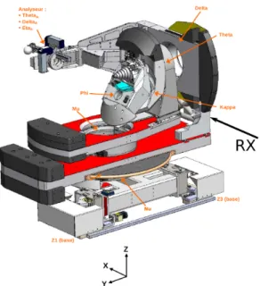
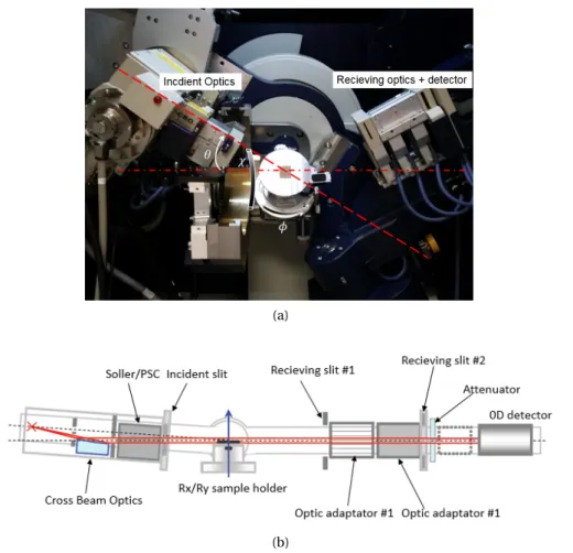
2.1.4 In-plane XRD measurements . . . 69 ix
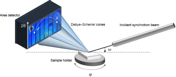
2.1.5 3D-Reciprocal space mapping . . . 72
2.1.6 Correction of the diffraction images . . . 77
2.1.7 Stitching and intensity correction . . . 81
2.2 STEM-EDS . . . 81
2.3 Conclusion . . . 82
3 Formation and stability of Ni-InGaAs 85 3.1 Introduction . . . 85
3.2 Experimental elements . . . 86
3.2.1 Sample preparation . . . 86
3.2.2 Substrate preparation and quality . . . 87
3.3 Results . . . 88
3.3.1 Electrical results . . . 88
3.3.2 Structure of the intermetallic . . . 89
3.3.3 Texture of the intermetallic . . . 92
3.3.4 Domain quantification of Ni/InGaAs/InP samples . . . 98
3.3.5 Distribution of elements in the intermetallics . . . 101
3.4 Discussion . . . 102
3.4.1 Texture of the Ni/InGaAs/InP intermetallic . . . 102
3.4.2 Texture anisotropy . . . 105
3.4.3 Origin of group A and group B domains . . . 108
3.4.4 Texture of Ni0.9Co0.1/InGaAs/InP . . . 110
3.4.5 Stoichiometry . . . 111
3.4.6 Superstructure of the Ni-InGaAs/InGaAs/InP . . . 113
3.5 Conclusion . . . 114
4 In situ X-Ray diffraction 119 4.1 Ramp annealing of the Ni/InGaAs/InP systems . . . 119
4.1.1 The Ni(20 nm)/InGaAs/InP system . . . 119
4.1.2 The Ni(7 nm)/InGaAs/InP system . . . 135
4.1.3 Discussion: On the effect of the film thickness . . . 142
4.2 Ramp annealing of Ni0.9Co0.1(20 nm)/InGaAs/InP . . . 142
4.2.1 Formation of the intermetallic . . . 143
4.2.2 Texture of the intermetallic . . . 146
4.2.3 Linear thermal expansion coefficients . . . 150
4.2.4 Discussion: on the effect of Co on the intermetallic formation . . . 152
4.3 Conclusion . . . 154
General conclusions and perspectives 157
Bibliography 172
Contents
Appendix B 175
Abstract
Cette thèse porte sur l’analyse microstructurale d’intermétalliques formés par réaction à l’état solide entre une couche mince de métal Ni(Co) et un substrat d’InGaAs et s’inscrit dans le cadre du développement de reprises de contact pour les dispositifs MOSFET sub-10 nm ou les applications photoniques. Ce travail comporte une partie relative au développement d’une méthodologie de diffraction des rayons x adaptée à ces composés très texturés et deux parties distinctes où nous décrivons et discutons les résultats expérimentaux. L’étude mi-crostructurale (phase, texture. . . ) des intermétalliques obtenus par réaction à l’état solide est rendue complexe par la formation transitoire de phases métastables, non stœchiométriques parfois, contraintes mécaniquement, et présentant en général des orientations cristallines (texture cristallographique) très marquées. Du fait de cette complexité microstructurale, ces intermétalliques n’ont souvent pas été caractérisés de façon complète et peu de connaissances se trouvent sur leur structure et leur formation. Aussi, et pour caractériser de façon complète et sans omettre des phases ou des orientations dans le système Ni-In-Ga-As, nous avons contribué au développement d’une méthode de mesure globale et rapide par diffraction des rayons X permettant de reconstruire une cartographie large 3D de l’espace réciproque. Les données recueillies par cette méthode sont reconstruites afin d’extraire soit des diagrammes de diffraction dits « détexturés », soit des figures de pôle. . . permettant une analyse semi quantitative de la microstructure des échantillons.
Dans la première partie des résultats expérimentaux, nous nous intéressons à la caractérisation des intermétalliques formés à partir d’empilements Ni/InGaAs/InP recuits ex-situ à différentes températures. Nous décrivons la formation des intermétalliques, leurs textures, et leurs paramètres structuraux. Nous relevons certains aspects de la microstructure qui évoluent en fonction de la température de recuit comme l’anisotropie de texture, la stœchiométrie des intermétalliques et le domaine d’existence thermique et nous proposons des hypothèses qui peuvent expliquer l’évolution de ces phénomènes. Cette première étude faite sur des substrats InP a été confrontée aux résultats obtenus pour des intermétalliques similaires réalisés sur substrats InGaAs/GaAs/Si. En effet, les substrats Si sont les substrats industriellement ciblés pour la réalisation de composés logiques à canal III-V à grande échelle (sur des plaquettes de 300mm de diamètre). Ensuite, nous avons comparé la métallisation de la couche d’InGaAs dans le cas de Ni pur avec la métallisation d’InGaAs lorsqu’un élément d’alliage (Co) est ajouté à la couche de Ni. Ainsi, l’analyse microstructurale révèle des différences notamment sur
les textures qui ont été interprétées sur la base de considérations thermodynamiques, mais aussi structurales comme l’alignement des deux couches entre elles, liées à des aspects plus cinétiques.
Dans la deuxième partie de ce travail, nous présentons les résultats des analyses in situ effectuées par cartographies de l’espace réciproque en 3D au synchrotron ESRF à Grenoble. Il s’agit de suivre en temps réel par diffraction des rayons X, les réactions à l’état solide des échantillons du type Ni (7 nm et 20 nm)/InGaAs/InP et Ni0.9Co0.1(20 nm)/InGaAs/InP lors de
recuits par rampes... Ensuite, nous avons effectué des recuits isothermes sur les échantillons de type Ni (20 nm)/InGaAs/InP. Ces différentes mesures, couplées avec des hypothèses sur la croissance nous ont permis d’extraire les paramètres cinétiques relatifs à la formation de la première phase d’intermétallique. Les textures observées et leur évolution lors des recuits thermiques in situ sont différents des recuits ex situ. Ceci peut notamment être expliqué par un mode de recuit différent dans le cas in situ où la cinétique du système est plus lente, favorisant ainsi des structures et textures qui pourraient êtreplus stables.
Contents
This thesis focuses on the microstructural analysis of intermetallics formed by solid-state reaction between a thin layer of Ni (Co) metal and an InGaAs substrate and was carried out in the framework of contact development for sub-10 nm MOSFET but have also photonic applications. This work includes a part related to the development of an X-ray diffraction methodology adapted to highly textured compounds and two distinct parts in which we describe and discuss the experimental results.
The microstructural study (phase, texture ...) of intermetallics obtained by solid-state reaction is complicated due to the formation of transient metastable, often non-stoichiometric and me-chanically stressed phases. These phases have generally very marked crystalline orientations (crystallographic texture). Because of this microstructural complexity, these intermetallic have often been not fully characterized and there is little knowledge about their structure and formation. Moreover, and to fully characterize the Ni-In-Ga-As system without omitting phases or textures, we have contributed to the development of a comprehensive method of rapid measurement by X-ray diffraction to reconstruct large 3D maps of the reciprocal space. The collected data through this method are reconstructed to extract either diffraction diagrams called "detextured" diagrams or pole figures ... which allows a semi-quantitative analysis of the intermetallic microstructure. In the first part of the experimental results, we focus on the characterization of intermetallic formed through Ni / InGaAs / InP stacks and annealed ex situ at different temperatures. We describe the formation of the intermetallics, textures, and structural parameters. We note some aspects which vary depending on the annealing temperature such as the texture anisotropy, the stoichiometry of intermetallic and range of thermal existence and propose hypotheses that can explain the evolution of these phenomena. The studies on InP substrates were compared to results obtained for similar intermetallic made on GaAs / Si substrates. Indeed, the Si substrates are targeted for industrials to achieve logic compounds III-V channel large-scale (on 300 mm wafers). Then, we compared the metallization of the InGaAs layer in the case of pure Ni metallization with the results when an alloying element (cobalt) was added to the Ni layer. The microstructural analysis revealed several differences especially texture differences. These differences were interpreted on the basis of thermodynamic considerations, but also on the basis of structural alignment of the two layers together which are also linked to more kinetic aspects.
In the second part of this work, we present the analysis results of studies performed by in situ 3D Reciprocal Space Mapping on the ESRF synchrotron in Grenoble. We followed the formation and stability of the intermetallics by real-time X-ray diffraction measurements, for different kind of samples: Ni (7 nm and 20 nm) / InGaAs / InP and Ni0.9Co0.1(20 nm) / InGaAs
/ InP, using ramp annealing... Then, we performed isothermal annealings for Ni(20 nm) / InGaAs / InP samples. These measurements, coupled with assumptions on the intermetallic growth, allowed us to extract the kinetic parameters for the formation of the first phase of the intermetallic. The observed textures and their evolution during in situ thermal annealings are different than ex situ annealing. This can be explained by a different mode of annealing in the case of in situ where the kinetics of the system is slower, thus favoring the most stable structures and textures.
Introduction générale
En réduisant la taille des dispositifs électroniques à base de Si à des dimensions nanométriques, les transistors MOSFET (Metal Oxide Semiconductor Field Effect Transistor) atteignent leurs limites fondamentales. En effet, bien que les limites relatives aux procédés de fabrication aient été largement surpassées (notamment en ce qui concerne la résolution d’impression de photolithographie qui a été amplement améliorée), les limites physiques relatives au Si et le comportement des porteurs de charge à des épaisseurs extrêmes sont difficilement surmontables. Une deuxième problématique liée aux dispositifs à base de silicium est la problématique de dissipation de puissance à l’état statique de transistor (la puissance statique servant à maintenir les états logiques à leur valeur entre une permutation de signal). En effet, la dissipation est reliée aux courants de fuites dans le dispositif, ces courants étant inévita-bles. Cette problématique est d’autant plus importante lorsque les transistors sont de taille nanométrique et leur densité d’intégration extrêmement élevée ce qui provoque des prob-lèmes de surchauffe. Ainsi, il s’avère que les prochains nœuds technologiques des transistor CMOS soient compliqués à concevoir du fait des propriétés intrinsèque du Si. Cependant, deux solutions majeures s’offrent pour pallier à ces problématiques. La première solution con-sisterait à revoir l’architecture des transistors planaires « classiques » et à imaginer de nouvelles architectures, moins couteuses en termes d’énergie de fonctionnement et qui permettent de mieux contrôler les courants de fuite. Cette solution est plus ou moins aboutie et se manifeste dans les transistors à canal enfouit FD-SOI (Fully Depleted Silicon On Insulator), des transis-tors dits « tri-gate » où le contrôle de courant dans la grille (et donc du champ électrostatique agissant sur les porteurs de charge dans le canal) se fait non pas par une seule direction, mais par trois directions à la fois. Une deuxième solution aussi intéressante que radicale est le changement de matériau de canal en remplaçant le silicium par un matériau qui offre une mobilité de porteurs de charge plus importante. En effet, si la mobilité de porteurs de charges est plus importante, il serait possible de fournir moins d’énergie pour le fonctionnement du transistor et continuer à obtenir des performances acceptables pour le nœud technologique visé. A cet effet, les composés III-V, et notamment les composés InxGa1−xAs constituent des
candidats idéaux pour remplacer le silicium. En effet, ces composés présentent une mobilité de porteurs de charge par rapport au silicium (à titre d’exemple, la mobilité des porteurs de charge de l’In0.53Ga0.47As est environ 10 fois supérieure à celle du Si).
Les possibilités de fabrication de composants microélectroniques à base de matériaux III-V
ont commencé à être explorées pendant les années 60. Cependant, la piste des matériaux III-V a été délaissée à cause des oxydes à l’interface trop compliqués à graver. Toujours est-il, des études récentes ont réussi à démontrer la capacité à surmonter cette problématique et la faisabilité des transistors MOSFET à base d’InGaAs à échelle nanométrique. Ces études encourageantes ont aussi démontré en pratique que les performances des transistors MOS à canal III-V sont meilleures que les performances des transistors à canal Si à échelle réduite. Cependant, de nombreuses difficultés restent à surmonter et de nombreuses étapes de fab-rication du transistor restent à étudier pour pouvoir aboutir à un procédé industriellement viable.
Parmi ces problématiques se trouvent les problématiques de la grille, du nettoyage de la couche de canal ainsi que la problématique de la reprise de contact à la source et au drain. L’une des problématiques majeures est l’injection de courant dans le canal aux niveaux des sources et drains. La réalisation de contact métal/Semiconducteur de faible résistivité et compatible avec les procédés industriels en vigueur est une problématique de premier plan. Cette dernière problématique constitue le sujet d’étude de cette thèse. Ainsi nous allons nous intéresser dans cette thèse à l’étude de la formation et la stabilité d’intermétalliques formés par réactions à l’état solide entre un métal ultrafin et une couche d’InGaAs
Ainsi, dans le premier chapitre nous allons tout d’abord décrire des généralités sur les réac-tions à l’état solide dans le cas des couches minces ainsi que la formation et la cinétique de formation de phases. Ensuite, nous allons étayer les différents éléments de bibliographie sur GaAs et sur InGaAs. Ces éléments constituent une base de compréhension indispensable pour ce travail, mais montrent aussi les questions soulevées par les travaux sur les composés Ni-GaAs et le débat qui s’en est suivi, notamment en ce qui concerne la séquence de phase et la définition des intermétalliques formés.
Dans le deuxième chapitre nous allons décrire le dispositif expérimental qui a été mis en place pour pouvoir étudier les intermétalliques formés par réactions à l’état solide entre un métal (typiquement le Ni). En effet, cette thèse se déroule dans un contexte de développement d’une technique de caractérisation de diffraction de rayons X qui permet de scanner rapidement et de manière quasi-complète l’espace réciproque. En réalité, il est difficile de caractériser ce type d’intermétallique, dont il existe peu de littérature dessus, par des moyens de diffraction de rayons x classiques. Les couches minces formées sont souvent texturés et une caractérisation par DRX symétriques ne peut être suffisante pour les définir. Ainsi, nous décrivons dans ce chapitre les éléments nécessaires pour comprendre la technique de caractérisation développée : les cartographies de l’espace réciproque en 3D.
Dans le troisième chapitre, nous nous intéressons à l’étude ex situ des intermétalliques formés sur pleine plaque par réactions à l’état solide entre une couche ultra-mince sur de Ni et une couche d’InGaAs sur un substrat d’InP. Nous décrivons dans ce chapitre l’évolution des textures, des paramètres structuraux, de la composition, de la séquence de phase, de la résistivité et de la qualité interfaciale des films d’intermétalliques formés en fonction de la
Contents
température de recuit. Nous nous intéressons par la suite à l’effet du substrat sur la formation de l’intermétallique en étudiant cette fois-ci des empilements Ni/InGaAs/GaAs/Si1. Enfin, nous nous intéressons aux effets d’ajout d’autres éléments sur la couche de Ni pur en l’alliant avec du Co. En effet, réaliser des alliages peut changer considérablement certains paramètres de l’intermétallique comme la stabilité thermique ou la température de formation.
Dans le quatrième et dernier chapitre, nous décrivons les résultats des études in situ des intermétalliques. Ces études ont été réalisés au synchrotron ESRF à Grenoble et ont permis de décrire avec plus de détails la formation et l’évolution de l’intermétallique en fonction de la température de recuit. Ces études ont aussi permis de mettre en évidence l’effet de l’alliage ainsi que celui de l’épaisseur sur la formation de l’intermétallique. Finalement, nous décrivons les paramètres cinétiques qui ont été calculés à partir des mesures d’isothermes de températures sur des échantillons Ni/InGaAs/InP.
1En effet, le substrat visé est le Si. Si notre étude porte majoritairement sur des empilements de type
Ni/In-GaAs/InP, c’est parce que ce type d’empilement offre la meilleure qualité cristalline pour la couche d’InGaAs et constitue ainsi des conditions idéales de croissance d’intermétallique.
Introduction
Motivations and challenges of nowadays Si-based devices
Si-based microelectronics is reaching fundamental limits when it comes to scaling new devices. While process-related limits were stretched to extraordinary horizons (photolithography resolution is barely a problem for CMOS fabrication), the limits are deeply related with the physical properties of Si and the behavior of charge carriers in extremely thin films. While we will not address solution related to Si-components or Si-based materials in this work, we think it is important to enumerate some relevant challenges that justifies Si replacement. Indeed, understanding these limits help us define the motivations to replace silicon with III-V materials.
Short-Channel effects
The reduction of the gate length to ultimate scales causes the emergence of parasitic electro-static effects called short-channel effects. These effects disturb the control of the conductivity between the drain and the source by the applied potential VGS between the gate and the
source [1]. In fact, when transistors are downscaled, the source and drain are brought closer. This is problematic because one also brings closer the drain-substrate and source-substrate depletion regions (see Figure 1). Normally, these depletion regions are an obstacle for current towards the substrate. The major charge carrier in the source and drain regions will encounter a potential barrier that prevents them from diffusing into the bulk (and eventually the same thing for the major charge carriers in the bulk towards the source and drain). When VDS
increases (the potential between the source and the drain), the drain-substrate depletion region widen and can, in case of low lG (gate length), join the source-substrate depletion
region: this is called the punch-through phenomena (see Figure 1). The potential barrier at the source-substrate frontier shrinks and the major charge carriers from the source can diffuse under these conditions into the substrate and then drift into the drain-substrate depletion zone. Thus, a leakage current passing through the substrate between the source and the drain is established. In this case, the diffusion current is no longer controlled by the gate.
Figure 1 – Illustration of the punch-though phenomena in the case of a blocked NMOS.
Gate Insulator Thickness
Silicon dioxide has remained for several decades the preferred gate insulator for Si-based MOSFETs. SiO2was downscaled to fit recent technological nodes from 300 nm for 10µm to
1.2 nm for 65 nm technological nodes. This thickness reduction of the oxide is important in order to have a larger Cox(Oxide capacitance) and thus having a larger Ion(ON current) which
in its turn helps to maximize the circuit speed. However, beyond 1.5 nm, tunneling leakage occurs. Indeed, at 1.2 nm, SiO2leaks 103A/cm2. Therefore, if an IC chip contains 1 mm2
of 1.2 nm SiO2thin film, the oxide leakage alone would reach 10 A. This current leakage is
sufficient to drain a cell phone battery in few minutes.
Introduction of III-V compounds in logical devices
Substrate problematics
One of the major problematics preventing the use of InGaAs alloys is the possibility of making good quality epitaxial layers of III-V materials on a substrate that respects some criteria. The corresponding criteria are robustness of the substrate, economically viable and of course the possibility to grow good quality InGaAs on top of it. InP might seem to be good a candidate as a substrate, especially because its lattice parameter matches the one of In0.53Ga0.47and thus
allows high quality epitaxy of III-V materials on it. Alas, InP is highly expensive, it is fragile and is not available in 300 mm wafers. Moreover, InP substrates would be incompatible with most Si tools used nowadays in the semi-conductor industry because it would require special holders to fit in 300 mm-tools. One solution is to figure out the technology to obtain good epitaxial InGaAs layers on Si substrates. The pre-deposition of buffer layers before the III-V material is a way to minimize the defects in the active III-V area and help absorb the crystal-lographic dislocations. Since InGaAs is polar on some of its planes and direction (because it yields a non-centrosymmetric zinc-blende structure), special care to the homogeneity of the III-V bulk. Recent extremely encouraging results showed the possibility of the control of the occurrence of anti-phase domains in GaAs deposited on Si using low miscut substrates [2].
Contents
Scaling issues
The continuous down-scaling of transistors is driven, not only by the gate shrinkage, but also by three essential characteristics. First of all, dimension reduction which allows higher integration density. Then, the switching energy and the switching speed. Dimension and switching energy continued to decrease while integration density and switching speed has continued to increase. With decreasing dimensions, dynamic and static power dissipation increase. Here, we refer to the power dissipation associated with the switching of logic states as dynamic power. While the static power refers to the power spent to maintain logical states at their value between state switching. Static power dissipation is related to current leakage within the device and cannot be avoided. With the increase of integration density, power dissipation has become a major problem of CMOS-based electronic devices and the MOSFET scaling has entered the “power-constrained scaling” era. Indeed, it requires robust packaging and cooling in order to enhance the device performance at lower scales. One way to solve this problem is to reduce the switching energy, thus the operating voltage, between two states. Ultimately, reducing the operating voltage will impact the switching speed of the CMOS. In order to solve this dilemma, the introduction of a new channel material can be considered [3, 4]. Indeed, III-V materials and especially InGaAs and GaAs materials present remarkable mobility of charge carriers compared to silicon. For example, the mobility of charge carriers in In0.53Ga0.47As compounds is 10 times higher than in Si (see Figure 2). In this case, a reduction
of the operating voltage will much less impact the switching speed, and the integration density can follow its original trend in time.
Figure 2 – Electron and hole mobility of group III–V compound semiconductors. The highest room-temperature mobility of electrons (red) and holes (blue) in inversion layers and quantum wells is shown as a function of the actual semiconductor lattice parameter [5].
The possibility of using III-V compounds in ultimate scaled devices was recently reviewed [5]. J. Del Alamo reports the most recent attempts to realize a III-V functional MOSFET device. The
best device performance was obtained on InGaAs burried-channel structures equipped with an InP barrier layer using Atomic Layer Deposited (ALD) TiSiO as the dielectric [6]. This 75 nm device displays outstanding performances in regard to the current drive and subthreshold characteristics, even in comparison with state-of-the-art silicon MOSFETs. Moreover, Del Alamo lists the general problematics that should be solved in order to make reliable III-V MOSFETs. Some of these problematics will be discussed in the following sections.
The electrical performance and possible issues of III-V MOSFET compounds can be tackled through the acquired knowledge on III-V HEMT (High-Electron-Mobility-Transistors) de-vices [7]. In fact, III-V HEMT dede-vices are widely spread, and the industry is quite mature when it comes to III-V integrated circuits. This spread is largely due to mobile devices and their highly demanding data treatment requirements. InGaAs and InAs HEMTs present injection velocity (vi n j) of 4.1 cm.s−1at an operating voltage of 0.5 V which is approximately 2 times
higher than vi n j of strained Si at an operating voltage of 1 V [8].
Nevertheless, the comparison of III-V HEMT devices and possible III-V logic devices remain limited as HEMT devices tolerate high gate leakage and are mainly bulk-based devices whereas III-V logic devices are targeted to be thin film-based devices. Moreover there are several critical issues that a possible switch from Si to III-V device will trigger. As it is the case for Si-based MOSFETs, gate insulator thickness and short-channel effects are very serious challenges for III-V materials. However, literature has reported encouraging results on practical III-V FET transistors. Indeed, III-V quantum-well FETs have higher intrinsic speed, i.e., lower gate delay CV/I, and lower energy delay product than Si MOSFETs at a given transistor gate length LG[9].
Gate Stack
Gate stack is crucial in the MOSFET design and consists of a metallic gate, a dielectric layer to prevent current leakage and the semiconductor itself. Historically, the choice of silicon as a channel material was much a result of the excellent qualities of its native oxide. Indeed, SiO2has remained for several decades an excellent choice as a gate dielectric: easy to control
and to form. Alas, no equivalent gate oxide exists for III-V materials. In fact, III-V oxides result in a pinning of the Fermi level [10]. Fermi level pinning remains a nemesis for electrical engineers and results ultimately in the inability to modulate the electrostatic field inside the semiconductor. This phenomenon induces reverse band bending and thus initiate the production of electrical fields that deflect charge carriers from the channel into the interface states where they are annihilated. Thus, it is impossible to directly use III-V native oxides for MOSFET elaboration. GaAs remain the most mature III-V material used to elaborate MOSFETs and proposed solutions included the in situ deposition of oxides such as Ga2O3[11, 12], which
proved to be efficient to enhance device performances. Atomic Layer Deposition (ALD) of Al2O3allowed obtaining of good quality ex situ deposited gate dielectric. The ALD was efficient
even with the presence of native III-V oxides on top of GaAs surface as a “clean-up” effect takes place during the deposition and the oxide is eliminated [13, 14]. Such results permitted
Contents
the realization of sustainable InGaAs MOSFETs [15]. Interface states are inevitable in such deposition conditions. Nevertheless, several interface engineering solutions were proposed. These solutions are maily inspired by the progress made on silicon MOSFETs and consist of the deposition of interfacial layers, post-deposition treatment and pre-cleaning. The interface quality can also be engineered through substrate orientation. Indeed, better interface quality and device performances were obtained using (1 1 1) GaAs oriented substrate rather than (1 0 0) oriented substrate [16].
It was also demonstrated that Indium addition into GaAs improves drastically the MOSFET performance and that the best results are obtained for InAs MOSFETs [17]. Gate stack scaling must also take into consideration channel mobility. Indeed, dielectric/semiconductor inter-face can present roughness and interinter-face state eventually induce Coulomb scattering that degrades charge carrier mobility inside the channel. A buried-channel can help solving this problem by interposing a wide-band semiconductor channel between the channel and the oxide [18]. This solution has yet to be experimented on very short devices.
There is a lot of different ways to exploit in order to engineer proper gate stacks for III-V MOSFETs. GaAs-based devices are the most mature MOSFETs, and taking benefit from the science on these devices, along with the mature experience on III-V HEMTs and actual silicon technologies, it is not foolish to imagine boosting the research towards elaborating industrially-scaled, reliable and reproducible gates for very short channel devices.
Yet other critical issues remain to be solved and understood. In the next paragraph we will introduce the contact issue for III-V logical devices. First of all we will review contact elabora-tion for III-V HEMTs. Then we will enumerate the metallizaelabora-tion of GaAs bulks. Finally, we will present the very recent results on InGaAs metallization.
Contact issues
One of the challenges for very short silicon MOSFETs is to minimize parasitic capacitance from one part of the transistor structure to another. This challenge remains the same if InGaAs MOSFETs are to be developed. InGaAs HEMTs have a source resistance of 150-200Ω/µm [5], yet extremely short-scaled devices require a source resistance below 50Ω/µm [5]. While HEMTs are large devices, scaling down the device dimension does not help getting a lower resistance as simulations on such devices demonstrate [19]. A self-aligned silicide-like process is likely the most promising solution in order to reach source resistance as low as 50Ω/µm. Indeed there are two major ways to form ohmic contacts. One can consider unreacted contacts and the heat-treated contacts. Unreacted contacts are directly deposited on the substrate and must not be exposed to overheat or else the deposited contact layers would intermix or be dissolved into the substrate. Heat-treated contacts on the other hand are obtained by depositing a metallic layer on the substrate, and then making this layer react with the bulk by giving it enough thermal budget. A solid-state reaction occurs and new phases are formed including intermetallic phases. These intermetallic phases can indeed form a suitable ohmic
contact for the MOSFET.
We will be interested in the formation of intermetallics by solid-state reaction between metals and III-V compounds. This kind of reaction has been reported in literature especially for GaAs and AlAs [20–24]. There was a dense work to characterize GaAs intermetallics since the mid-1980. Pd, Co, Pt and especially Ni are widely scoped as metal candidates [25]. Aside from electrical performances, there was also a great need to understand the so-formed material from a phase/phase sequence/texture/thermodynamics point of view. The understanding of the material is of great importance to correctly scale process steps. Indeed, when it comes to thin films, there is an utmost need to control the phase formation and interface unifor-mity of the intermetallic. The so-formed phase upon solid-state phase reaction must be in thermodynamic equilibrium with the substrate so that the contact stays stable, uniform and reproducible. In the following section we will be interested in the material characterization of Ni-GaAs intermetallics which has been widely explored. These early results on GaAs are important and constitute crucial information at the beginning of this work. Indeed, Indium is completely miscible in the InGaAs zinc-blende structure and Ni-InGaAs intermetallics can be regarded, to a certain extent, as a ternary system.
Conclusion
Silicon has reached its limits as a channel material and one solution, among others, is to replace it with a material that allows reaching higher mobility of charge carriers in the channel. Changing the channel material issues new challenges however. Among these challenges is the formation of contact materials for III-V MOSFET devices. From a process point view, one would like to make a silicide-like process and to make contacts following a solid-state reaction between the metal and the III-V material. The so-formed intermetallic can be optimized in order to present better uniformity, resistivity or interface. The target channel substrate is ideally the In0.53Ga0.47As substrates. This stoichiometry choice is not arbitrary since it is
exactly at In0.53Ga0.47As that the InxGa1−xAs lattice parameter perfectly matches the lattice
parameter of InP and thus can be easily studied on InP substrates. Therefore a great deal of the hereby work is done on InP substrates with the latter proportion of In and Ga. However, on the long term, Si substrates must be targeted, and issues related to such substrates, such as III-V bulk defects and antiphase domains must be addressed. The present work does clearly not claim to present a process related such as integration studies or electrical performance studies. Rather, we focused on studying the material itself in order to give key parameters to process people in order to properly form the contacts on future CMOS or power devices. Therefore, we will describe in this manuscript the solid-state reaction between Ni and InGaAs compounds. This reaction was barely studied and attempts to characterize the materials will be enumerated in Chapter 2 along with the already acquired science on similar reaction on GaAs layers. In
Chapter 2 we will also see a brief history of silicides because the outcomes of research on
silicides are fundamental to explain, understand and characterize intermetallics formed on InGaAs. In Chapter 3 we will describe the experimental procedure that was developed to
Contents
characterize such materials and explain the need to explore such materials through methods like 3D-Reciprocal Space Mapping. Chapter 4 will deal with the phase formation and texture of the Ni-InGaAs intermetallic along with a discussion on the orientation of the intermetallic and influence of substrate on these orientations. The phase transition will be discussed in the light of the knowledge acquired on reaction of Ni with GaAs. Finally Chapter 5 will present the in-situ measurements results for the intermetallic and the kinetic parameters associated with the formation of Ni-InGaAs.
Résumé du chapitre 1
La réaction à l’état solide entre un métal et un substrat d’InGaAs a été peu étudiée. En effet, il y eu un regain d’intérêt pour les MOSFETs III-V, et typiquement, les MOSFETs à substrat InGaAs depuis les années 2010. Nous nous intéressons à une étape importante de la fabrication de ces composants électroniques logiques : la métallisation de la couche de semi-conducteur pour former des contacts à caractère ohmique à la source et au drain. Historiquement, la réalisation de cette étape sur Si se fait par réaction à l’état solide entre un métal (ou un composé métallique) et la couche de silicium pour réaliser des intermétalliques. La méthode la plus courante pour aboutir à des intermétalliques est le procédé SALICIDE (self-aligned silicide2). Ce procédé permet d’obtenir des intermétalliques sans recourir à des étapes supplémentaires de photolithographie. De nombreux métaux, ou composés de métaux ont été utilisés pour réaliser des intermétalliques sur Si. Parmi les intermétalliques les plus étudiés et les plus utilisés par l’industrie de la microélectronique nous retrouvons le CoSi2, le TiSi2, et le NiSi. A
chaque nœud technologique, les conditions de dépôt et de recuit de l’intermétallique doivent être réétudiées afin de se conformer aux performances attendues du dispositif électronique en terme d’épaisseur, de régularité d’interface et de résistivité. En atteignant des épaisseurs limites de la taille grille (et donc fatalement d’épaisseur limite de l’intermétallique formant la reprise de contact), des limitations physiques se mettent à se manifester. Ainsi au-delà de 200 um, le TiSi2présente une résistivité trop élevée liée à un changement de phase. Le
CoSi2présente, quant à lui, des interfaces non uniformes une fois l’épaisseur du métal déposé
atteint une épaisseur limite.
Dans ce chapitre, nous nous intéressons tout d’abord à la description de la réaction à l’état solide entre un couple d’éléments. On énumère les régimes de croissance qui peuvent être linéaire, parabolique ou encore dans la plupart des cas, des régimes linéaire-paraboliques. Ces différents régimes peuvent être formalisés en fonction du taux de réaction, de l’énergie d’activation ainsi que le taux de réaction maximal. Dans le cas d’un régime linéaire, l’épaisseur de la phase formée est très faible et ne limite pas la réaction. Dans ce cas, la croissance est limitée par la réaction à l’interface. Dans le cas d’un régime parabolique, l’épaisseur de la phase formée entre le couple est importante. Ainsi la croissance n’est plus limitée par la réaction à l’interface mais par la diffusion à l’intérieur de la phase formée. Ce chapitre est aussi l’occasion d’énoncer aussi les notions qui permettent de comprendre l’alignement de
2Siliciure auto-aligné.
couches minces. Ainsi, les couches minces peuvent être épitaxiées, avoir une texture de fibre, ne pas avoir de texture, mais aussi et plus récemment il a été démontré que des couches minces peuvent avoir des textures axiotaxiales. La réaction à l’état solide entre Ni et une couche de GaAs a été largement étudiée depuis les années 80 et jusqu’aux années 90. Plusieurs études se sont intéressées à l’établissement de diagramme de phase ternaire Ni-Ga-As. Les résultats de ces études présentent plusieurs différences notamment en ce qui concerne la définition des phases et des domaines d’homogénéités des phases d’intermétalliques formés. En effet, le travail de Guérin et Guivarc’h sur des poudres d’intermétallique Ni-GaAs démon-tre l’existence de 5 phases d’intermétalliques toutes hexagonales et appartenant au groupe d’espace P63/mmc. Ces phases se distinguent par des domaines d’homogénéité assez larges
et ont des stichométries allant de Ni3GaAs jusqu’à NiAs. En plus, un ordre/désordre s’établit
lorsque ces phases sont formées en fonction de la nature de la phase. Ces intermétalliques peuvent aussi être caractérisés par le rapport axial c/a et sont toutes métastable à l’exception de NiAs et de son extension en solution solide. Le travail de Zheng, publié simultanément aux travaux de Guérin et Guivarc’h, définit les phases d’intermétallique autrement. En effet, Zheng considère qu’une seule phase ternaire existe (la phase Ni3GaAs) et considère que les autres
phases avec des stœchiométrie entre Ni3GaAs et NiAs ne sont que des phases binaires avec
des solubilités ternaires plus ou moins importantes. Zheng n’exclut pas aussi que certaines phases, à priori hexagonale, soient en fait des phases monocliniques déformées vu la grande ressemblance de symétrie entre les deux groupes d’espace considérés. Finalement, les travaux d’Ingerly et al. en 1996 sur le système Ni-Ga-As débouchent sur un nouveau diagramme de phase et démontrent que toutes les phases formées sont des phases binaires avec des extensions ternaires très larges. Quel que soit l’étude sur Ni-GaAs, il en ressort que toutes les phases formées dans ce système sont métastables à l’exception de la phase NiAs. Ces différentes études réalisées sur des poudres montrent aussi la difficulté de caractériser les intermétalliques formés sur III-V.
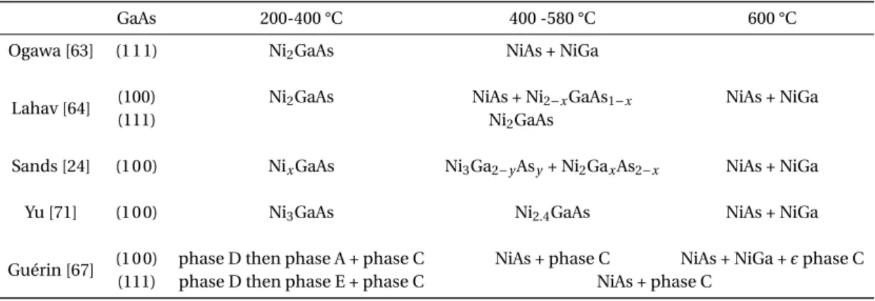
D’autres équipes se sont intéressées plutôt à la formation de l’intermétallique en couche minces en faisant réagir une couche de Ni avec un substrat InGaAs. Ces études démontrent que le premier intermétallique se forme généralement à basse température (entre 200 °C et 250 °C) et que ce premier intermétallique formé est généralement celui qui est riche en Ni (Ni3GaAs). Les intermétalliques formés sont fortement texturées (i. e. présentent
une orientation préférée) et présnetent l’orientation suivante : (0 0 0 1)Ni2GaAs||(1 1 1)GaAs ;
[1 2 1 0]Ni2GaAs||[1 1 0]GaAs La séquence de phase est différente selon les auteurs et cette
dif-férence s’explique surtout par des conditions de dépôt/recuits différentes. La tendance générale est que, au fur et à mesure que la température de recuit augmente, le ratio axial
c/a de l’intermétallique hexagonal augmente et l’intermétallique passe d’une structure
hexag-onale riche en Ni à basse température à une structure hexaghexag-onale NiAs, moins riche en Ni, à haute température. La plupart des auteurs rapportent aussi la formation de composés binaires cubiques NiGa à la fin de la réaction. Quant aux travaux sur la réaction à l’état solide entre un film mince et un substrat d’InGaAs, elles restent assez limitées. Les études sur ce sujet portent sur la formation d’intermétallique à basse température (entre 200 et 350 °C). Tout comme le
Contents
Ni-GaAs, les études sur Ni-InGaAs démontrent la formation d’un intermétallique hexagonal fortement texturé. L’intermétallique possède un caractère ohmique et une orientation dif-férente de celle qui a été rapporté pour Ni-GaAs. Ces études restent incomplètes de par au moins deux aspects : la caractérisation de l’intermétallique s’est faite la plupart du temps en analysant une partie limitée de l’espace réciproque. En effet, et de par l’aspect texturé des films formés, il est tout à fait possible d’omettre certaines phases ou orientations si une analyse complète de l’espace réciproque par diffraction des rayons X n’est pas effectué. Ceci a été longtemps le cas pour certaines phases de siliciures comme la phaseθ, longtemps considérée comme ayant une symétrie orthorhombique alors qu’elle possède une symétrie hexagonale ou encore les germaniures comme la phaseγ dont la symétrie hexagonale a été récemment démontrée. Le deuxième aspect manquant à ces études est l’aspect relatif à la formation et stabilité des intermétalliques. En effet, la plage de recuit rapportée par la littérature est limitée. Ainsi, une séquence de phase et un modèle d’évolution de stœchiométrie et/ou de phase n’a pas pu être rapporté. En plus, aucune étude in situ n’a été faite pour extraire les paramètres cinétiques relatifs à la formation de ces intermétalliques.
Finalement, il y a une nécessité d’une part de faire une étude qui se base sur une analyse complète de l’espace réciproque par une méthode rapide et appropriée. D’autre part, il est nécessaire d’effectuer une étude exhaustive ex situ et in situ pour mieux comprendre les mécanismes régissants la formation et la stabilité de ces intermétalliques.
1
State-of-the-art and issues
In this first chapter, we will first define the solid-state reaction (SSR) between materials and the diffusion treatments that are involved during an SSR in the case of thin films. We will then be interested in a particular step in the elaboration which is the intermetallic formation on top of the source and drain of MOSFETs. Hence, we will describe the SSR between metals in the case of a MOSFET and Si along with the SALICIDE process. Previous studies of Si-based intermetallics are valuable, not only because it gives insights on the solid-state reaction between metals and semiconductors for thin films, but also because important outcomes concerning the materials or the characterization methodologies were described or developed thanks to research on silicides. In the third part of this chapter, we will enumerate the previous studies of the SSR between metals and III-V materials. Especially Ni/GaAs and more recently Ni/InGaAs.
1.1 Solid-state reactions in the case of thin films
One can describe the evolution of the kinetics of a heterogeneous reaction in terms of two processes: separate nucleation and growth of the transformed regions. The nucleation process is classically explained by random fluctuation in a metastable assembly [26]. The earliest works on nucleation were conducted on the simplest case of a pure vapor condensed to form a liquid. A simple example of nucleation is the creation of water vapor from boiling water. The formation of the gaseous phase happens at temperature T above a critical temperature Tc.
Below Tc, the free energy of the liquid water is lower than the free energy of the vapor and
above Tcthe free energy of the liquid water is higher than the one of vapor. At T = Tcno phase
transformation can occur as both free energies of vapor and liquid water are equal (∆Gp= 0).
If∆Gp6= 0, then the most stable phase will nucleate. As the formation of a nucleus implies the
necessary creation of a new interface between the nucleus and the original system, the gain in volume free energy is counterbalanced by an increase in surface energy. As a result, the nucleation process is controlled by the competition between both contributions. The theory of nucleation from these earliest works was expanded to solid-state reactions.
Indeed, a similar situation is encountered when two bulk elements A and B are put into contact. Above a certain temperature Tc, a solid-state reaction occurs and germ-nuclei are
formed. After the formation of a germ-nuclei, the phase grows laterally along the surface until a uniform layer is formed. Then the phase grows normally to surface. Instead of the initial A/B system with one interface, the system presents now two interfaces A/AB and AB/B and two phases A, B and AB [27]. In our case, the growth of the phase is controlled by the diffusion of either metal atoms or In, Ga and As atoms through the so-formed phase, then, controlled by the chemical reaction between reactants at the interface leading to the formation of the new phase.
1.1.1 Diffusion mechanisms
The diffusion of atoms is the phenomenon of matter transportation under the effect of a gradi-ent of chemical potgradi-ential that is often considered equivalgradi-ent to a gradigradi-ent of concgradi-entration. In fact, the motion to another site is possible only when the neighbor site is vacant: it is the vacancy diffusion. If the atom is sufficiently small, then a diffusion through interstitial sites can be considered: it is the interstitial diffusion (see Figure 1.1).
Figure 1.1 – Schematic representations of (a) vacancy diffusion and (b) interstitial diffusion (adapted from [28]).
To jump from a site to another one, an atom must cross an energy barrier∆Gpwhich
corre-sponds to the free enthalpy or Gibbs energy and which is defined by:
1.1. Solid-state reactions in the case of thin films
∆H = ∆Hf+ ∆Hm (1.2)
∆H is the enthalpy change of reaction and is the result of the addition of the standard enthalpy of formation∆Hf and∆Hm, the enthalpy of migration of either atoms or vacancies. T and∆S
are respectively the temperature and the entropy.
The probability P of crossing the energy barrier is thermally dependent and is written:
P ≈ exp(−∆Gp
kT ) (1.3)
In the case of polycrystalline samples, the diffusion can be either a volumetric diffusion across the crystal, an inter-granular diffusion or a diffusion along the dislocation (which is also called pipe diffusion). The diffusion of atoms is generally faster along dislocations and grain boundaries than along the volume of the crystal.
1.1.2 Atom flux
When two bulks of species A and species B are put into contact, and in the presence of a gradient of concentration C, the atom flux J can be expressed using the Fick’s law:
J = −D ×∂C
∂L (1.4)
D is the coefficient of diffusion and follows an Arrhenius equation.
The migration of atoms of one species can be expressed through the gradient of chemical potentialµi, where i designates the species A or B:
Ji= −Xi× N ×
Di
kT ×
dµi
dL (1.5)
Where Jiis the flux of atoms i through the formed phase, Xithe atomic fraction of species i
in the phase, N the total number of atoms per unit of volume in the phase, k the Boltzmann constant and T the temperature.
1.1.3 Phase formation
Phase formation in thin films couples is regarded as sequential in opposition of simultaneous phase formation in bulk couples. Silicide studies have shown that often only one or two silicide phases are formed when a reaction occurs between the thin film couple [29–31]. Several treatments and approaches can be used to describe the phase formation.
1.1.4 Linear-Parabolic treatment
The linear Parabolic treatment was first used to describe the formation of silicon dioxide. Sev-eral authors including d’Heurle, Gas and Philibert [32, 33] have described the phase formation of thin films using this treatment.
1.1.4.1 Formation of one phase between materials A and B
If a compound AB grows between two pure elements A and B by the diffusion of A atoms (see Figure 1.2), one obtains the following equation:
Figure 1.2 – Schematic presentation of the AB phase growth between the pure elements A and B by the diffusion of A atoms.
JA= CA× MA×
dµA
dL (1.6)
Where the mobility is MA=DkTA, JAis the diffusion flux of element A, CAis the concentration
of element A,µAis the chemical potential of species A, L is the position or length of the AB
compound, DAdiffusion coefficient of the element A.
If one assumes that the intrinsic diffusion coefficient DAis not a function of the concentration,
we obtain: JA= CA× DA kT × ∆gA L (1.7)
1.1. Solid-state reactions in the case of thin films
Where∆gA
L is the Gibbs energy per A atom of the reaction A + B= AB. To be more specific, it is
the required energy to move one mole of A atoms from the A/AB interface across the AB layer to the AB/B interface. In other words, it is the driving force for diffusion∆µA.
Since we have: dL
dt = JA× νA (1.8)
WhereνAis the molar volume of species A.
and: CA= 1 νA (1.9) then: dL dt = DA× ∆gA kT × 1 L (1.10)
If we integrate the Equation 1.10, we obtain the parabolic growth law:
L2= Kdt (1.11)
Where Kdis the parabolic rate constant.
However, if we consider Equation 1.11 at very small layer thickness, then L ≈ 0 anddLdt ≈ ∞. Therefore, d’Heurle et al. [31–33] introduced the concept of linear-parabolic kinetics. The starting point is Equation 1.10. If we introduce a "kinetic parameter" to take into account reactions at the interfaces, then:
dL dt = DA× ∆gA kT × 1 L + K00 (1.12)
As the thickness of the layer approaches zero L → 0 then Equation 1.12 is rewritten:
dL dt ≈ DA× ∆gA kT × 1 K00 (1.13) 25
and if one integrate this equation, we obtain:
L2+ K0L = K (t + t0) (1.14)
Where K0= K00
Indeed, when the layer thickness increases and the reaction time becomes longer, then we retrieve the "normal" parabolic growth equation
L2→ ∞ ⇒ L2≈ K t (1.15)
1.1.5 Linear treatment
At the beginning of the reaction, the AB compound film thickness is small, and element A and B are always available through the two interfaces. Therefore, the limiting factor of the AB compound film formation is the reaction at the interfaces and the thickness can be written as the following:
L = Krt (1.16)
Where Kr (cm.s−1) is a constant characteristic of the interfacial reactions. This constant is
thermally activated and depends on temperature following the Arrhenius law expressed at equation 1.17:
Kr= Kr 0exp(
Ea
kT) (1.17)
Where Eais the energy of activation and Kr 0is a pre-exponential factor.
However, if the reaction goes further, the thickness of the AB compound film will increase and the path used by A and B elements to reach each interface will increase. Thus, the reaction at the interface will become less and less important.
1.1.6 Parabolic treatment
At sufficient AB layer thickness, we can consider that the growth of the AB compound is no longer controlled by the interface reactivity but rather by the number of atoms (or flux) reaching the interface. The thickness is then written as the following:
1.1. Solid-state reactions in the case of thin films
Where Kdis also a thermally activated constant and is expressed in cm.s−2.
1.1.7 Simultaneous and sequential growth
The sequential formation of phases is widely reported [32, 34, 35]. In the case of thin films, phase growth is usually sequential rather than simultaneous. The sequential growth can be explained by a competition between reaction kinetics at the interface and diffusion of metal in the growing phases. When two phases grow simultaneously, the variation of their thickness depends on the flux inside each phase. This couple of flux J1and J2is used to explain the
sequential growth of phases. Hereby, we will present the equations that describe simultaneous growth, then, we will present those that describe sequential growth.
1.1.7.1 Simultaneous growth
Several phases appear at the same time in the case of simultaneous growth. Figure 1.3 presents a scheme of the simultaneous growth of two phase A2B and AB by solid state reaction between
a metal A and a semi-conductor B. In this example, we consider that diffusing species is the metal (so that JA»JB). The reactions occur at the two interfaces A2B/AB and AB/B.
Figure 1.3 – Schematic presentation of the simultaneous growth of two phases.
The flux J1represents the flux of A atoms in phase A2B and J1represents the flux of atoms
in AB. The growth of each phase does not depend only on the characteristics of the phase (reaction kinetics, diffusion coefficient), but also on characteristics of all the phases present in the diffusion couple A/B. The growth of the phase A2B occurs at the interface A2B/AB and
follows the following reaction:
A + AB → A2B (1.19)
The growth of phase AB occurs at the interface A2B/AB and also AB/B. At the first interface,
the reaction frees one atom from A2B in the following way:
A2B → A + AB (1.20)
This atom diffuses through the phase AB to react with the semi-conductor at the second interface AB/B:
A + B → AB (1.21)
Hence, the reaction of formation and consumption happen simultaneously at different inter-faces. The thickness variations L1and L2of phases A2B and AB are related to the diffusion flux
J1and J2of the metal A in phases A2B and AB respectively by the following relationships:
dL1
dt = J1− J2 (1.22)
dL2
dt = 2J2− J1 (1.23)
This equation system shows that there is a coupling between the growth rate of different phases.
1.1.7.2 Sequential growth
The growth rate of a phase does not only depend on its intrinsic growth parameters but also depends on all the parameters of all forming phases. If one suppose that every phase present a linear-parabolic growth, one can suppose that the flux of atoms through the phase 1 (J1) is
limited by the process of diffusion whereas the flux through phase 2 (J2) is controlled by the
reaction rate : J1= Kd L1 and J2= Kr (1.24) Thus dL1 dt = Kd L1 − Kr anddL2 dt = 2Kr− Kd L1 (1.25) In this case, phase 2 begins to grow when the first phase reaches a critical thickness in the following manner [35]: dL2 dt > 0 and L1> Kd 2Kr (1.26)
1.2. Silicide contacts
For thin films, the critical thickness, that can be considered as controlled by the reaction rate of phase 2 and by the diffusion coefficient of the metal in phase 1, is often of the same order than the thickness of the metallic film. The metallic film is completely consumed before the appearance of new phases, which induces a sequential formation of phases.
1.2 Silicide contacts
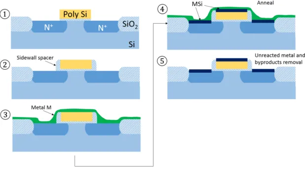
On top of the active zones of a MOSFET, there exists a “contact” zone made of an intermetallic that allows to make a physical and electrical link between the contact in the circuit and the active doped zones of the MOSFET. On silicon, these intermetallic contacts are called silicides. Silicides must meet some essential qualities in order to be integrated into circuits. The most important ones are the thermal stability and contact resistance of the silicide. Thus, it is important to understand the formation of the intermetallic in order to control its stability. Silicides are usually formed using a SALICIDE (Self-Aligned Silicide) process. This process consists of depositing a metal on top of the active regions and the gate, and making this metal react by bringing a thermal budget. The process is done simultaneously on these regions and an intermetallic is formed through solid-state reaction without need for further photolithography steps. Obviously, excess metal that did not react is removed using selective chemical etching. A SALICIDE process is illustrated in Figure 1.4.
Figure 1.4 – Salicide process steps and formation of the intermetallics on Source/Drain (S/D) regions and on the gate of the MOSFET.
Since their introduction in the 1970’s [36–38] in the CMOS fabrication process, silicides have constituted materials of choice when it comes to producing contacts for Si-CMOS devices. Indeed they generally present a low electrical resistivity, have good passivation properties and
can be thermodynamically stable. The qualities of a good silicide can be enumerated as the following:
• Thin film silicides according to the corresponding technological node; • Low resistivity (14µΩ for the 14 nm technological node);
• Low silicon consumption to prevent breaking through the junction or, in the case of Silicon on Insulator MOSFETs, breaking near the burried oxide layer;
• Thermal stability to avoid degradation at high annealing temperatures;
• Low thermal budget of formation to avoid degradation of already deposited layers of the device;
• Suitable growth constraints and thus suitable coefficient of thermal expansion; • Good quality of the interfacial layer, so that no agglomeration of the silicide occurs
(which causes resistivity degradation).
Literature on silicides is abundant and different materials were explored such as NiSi, PtSi, TiSi2, MoSi2, CoSi2. . . The microelectronic industry has used several types of silicides according
to the technological nodes and the evolution of needs in order to respect the criteria for having a good silicide contact. TiSi2has represented the main stream silicide contact up to the 0.2µm
technological node. However, beyond a certain width of lines, a limitation of the titanium sali-cide emerged. Indeed low resistance TiSi2is formed through a phase transformation from C49
(60-90µΩ/cm) to C54 (14-18µΩ/cm). Unfortunately, this transformation becomes extremely difficult for thin films, and hence, the so-formed Ti silicides are no longer suitable [39]. Then, cobalt silicide constituted a popular replacement for Ti silicides. Indeed, CoSi2needs a
lower thermal budget to be formed and up to a certain gate dimension, it does not suffer a degradation of resistivity at narrow lines. However, as the transistor gate length reaches the 50 nm, Co silicide suffers from a rise of resistivity and its Si consumption ratio becomes very important. Thus, nickel silicides were proposed [40]. Nickel silicides present very interesting features and meet most of the qualities required from a good silicide contact. NiSi has a lower density in Si compared to CoSi2and thus, Si consumption is limited during the solid-state
reaction. During the reaction, Ni is the diffusing species, and thus Si mobility is limited and bridging becomes less likely to happen. On top of that, NiSi has a much smoother interface than CoSi2which leads to lower resistivity, but also the possibility to get safely closer near
the buried oxide for SOI transistors. Finally, these silicides are fit for both Si and SiGe (low resistivity when reacted with both substrates) and thus can be used in a co-integration scheme of transistors.
The phase diagram of the Ni-Si system is rather complex and presents multiple stable phases at temperatures lower than 800 °C. Most of these phases are Ni-rich phases (Ni31Si12, Ni3Si,
![Figure 1.12 – Orientation of the hexagonal intermetallic as observed by Chen et al. [80] in an InGaAs Fin.](https://thumb-eu.123doks.com/thumbv2/123doknet/14527487.723118/60.892.209.717.147.372/figure-orientation-hexagonal-intermetallic-observed-chen-ingaas-fin.webp)