HAL Id: hal-01007327
https://hal.archives-ouvertes.fr/hal-01007327
Submitted on 19 Nov 2017HAL is a multi-disciplinary open access
archive for the deposit and dissemination of sci-entific research documents, whether they are pub-lished or not. The documents may come from teaching and research institutions in France or abroad, or from public or private research centers.
L’archive ouverte pluridisciplinaire HAL, est destinée au dépôt et à la diffusion de documents scientifiques de niveau recherche, publiés ou non, émanant des établissements d’enseignement et de recherche français ou étrangers, des laboratoires publics ou privés.
Strains, stresses and elastic properties in polycrystalline
metallic thin films: in situ deformation combined with
x-ray diffraction and simulation experiments
P. Goudeau, Damien Faurie, Baptiste Girault, Pierre-Olivier Renault, Eric Le
Bourhis, Pascale Villain, Frédéric Badawi, O. Castelnau, R. Brenner,
Jean-Luc Bechade, et al.
To cite this version:
P. Goudeau, Damien Faurie, Baptiste Girault, Pierre-Olivier Renault, Eric Le Bourhis, et al.. Strains, stresses and elastic properties in polycrystalline metallic thin films: in situ deformation combined with x-ray diffraction and simulation experiments. Materials Science Forum, Trans Tech Publications Inc., 2006, 524-525, pp.735-740. �10.4028/www.scientific.net/MSF.524-525.735�. �hal-01007327�
Strains, stresses and elastic properties in polycrystalline metallic thin
films: in situ deformation combined with x-ray diffraction
and simulation experiments
P. Goudeau
1,a, D. Faurie
2,b, B. Girault
1,c, P.-O. Renault
1,d, E. Le Bourhis
1,e,
P. Villain
1,f, F. Badawi
1,g, O. Castelnau
3,h, R. Brenner
3,i, J.-L. Bechade
4,j,
G. Geandier
5,k, N. Tamura
5,l1
LMP, Université de Poitiers, Avenue Marie et Pierre Curie, 86962 Futuroscope (France) 2 Netherlands Institute for Metals Research, Rotterdamseweg 137, 2600 GA Delft (Netherlands)
3
LPMTM (CNRS), Université Paris 13, av. J.B. Clément, F - 93430 Villetaneuse (France)
4
CEA-Saclay, DEN / DMN / SRMA / LA2M, 91191 Gif-sur-yvette Cedex (France)
5
ALS, LBNL, 1 Cyclotron Road, Berkeley, CA 94720 (USA)
a [email protected], b [email protected] c [email protected], d [email protected] e [email protected], f [email protected], g
[email protected], h [email protected], i [email protected],
jl
[email protected], k [email protected], l [email protected]
Keywords: Elasticity, thin films, size effects, diffraction, synchrotron, tensile testing, simulation.
Abstract. X-ray diffraction is used in combination with tensile testing for measuring elastic properties of metallic thin films. Size effect, elastic anisotropy and grain morphologies are considered in all these experiments and supported by different kind of numerical simulations operating at different length scales. Such instrumental studies are time consuming even if synchrotron sources are used. New experiments are under progress for reducing acquisition data and improving precision on strain measurements. After introducing briefly the main principles and results of our techniques, first promising measurements on nanometric W/Cu multilayers using 2D CCD detectors and high monochromatic flux at the Advanced Light Source Berkeley (USA) on beam line 11.3.1 are presented. In addition, simulation experiments for analyzing elasticity in textured gold film are discussed.
Introduction
X-ray diffraction is well-known as a trustworthy and powerful tool to determine the stress state of small-sized crystalline materials such as thin films. In addition, the use of x-ray sources with high brightness such as synchrotron radiation allows to tune the desired wavelength according to the expected measurement and to scan the sample surface with focus x-ray beam size smaller than 1 micron. It is a phase selective and a non destructive technique which allows determining both the mechanical behavior and the microstructure of diffracting phases. The elastic change in inter planar distance is used to determine the residual strains and stresses, owing that the stress free lattice parameters and elastic constants are known.
Since the 90’s, it has been shown that these two parameters depend strongly on film microstructure (nanometer grain size, high defects density, constraints caused by the substrate) which strongly relies on the way there are elaborated (physical vapor deposition, electro deposition, spin coating ….). Following previous examples, we developed a new method [1] combining X-ray diffraction and in-situ uni axial tensile tester for studying thin film mechanical behavior (Nature materials update, Research Highlights, June 27, 2002). First results have been obtained on the size
effects in purely isotropic tungsten thin films concerning elastic constants [2] and cracks propagation [3] in nanometric W/Cu multilayers. In order to extend the method capabilities, preliminary works have been down to study elastic behavior of strongly textured gold films deposited onto polyimide substrate using Crystallite Group Method (based on Reuss assumption) [4-7]. Nevertheless, due to the strong elastic anisotropy of gold and to the columnar structure inherent of thin films, suitable grain interaction model has to be used in order to better estimate or bound the elastic constants of thin films. In that frame, the use of homogenization methods is very helpful. Simulations using self-consistent model has been carried out and compared to experiments on textured gold films [8].
In that paper, we will first give a short overview of our works in that field, and in particular we will comment on new experiments on W-Cu multilayers for probing size effects. In a second part, we will discuss new results and perspectives concerning the effect of grain shape (morphological) texture on the elastic behavior of thin films.
Experimental
All samples have been prepared by ion beam sputtering. The gold and WCu multilayers films are deposited onto silicon substrates for initial characterizations (stress from curvature, period thickness with x-ray reflectometry, total thickness from a step profile, composition with extended dipersive x-rays in a scanning electron microscope ….) and on Kapton dog bone, 125 µm thick, for tensile testing. This polymer has been chosen for its weak young modulus (less than 5 GPa) and its large elastic domain.
X-ray diffraction experiments are performed in our laboratory using a 4-circles x-ray diffractometer with Cu Kα wavelength and a collimator of 1 mm2 and also at synchrotron beam lines at LURE Orsay (France), ESRF Grenoble (France) and more recently the Advanced Light Source (ALS) of the Lawrence Berkeley National Laboratory (LBNL) Berkeley (USA). In this last case, two-dimensional CCD detector has been used at beam line 11.3.1 [9] for recording x-ray diffraction patterns. An LaB6 standard reference powder deposited on the sample surface close to the region of interest allows very precise calibration of the whole diffraction geometry. The incident angle of the x-ray beam with respect to the sample surface is fixed to 14.4° and the photon energies used are 14518 and 13800 eV for gold and W/Cu films. These values allow to investigate (111) gold and (110) tungsten planes parallel to the sample surface. This is important in case of texture. A compact 200N tensile set up developed by Deben UK Ltd is adapted inside the goniometer for in situ deformation. The accuracy on the applied force is about 1% of the maximum value accepted by the load cell. In case of elastic regime measurements, we use a 20N load cell and then, the accuracy is 0.2N. For plastic regime, we used a 200N load cell. Figure 1 shows the tensile set up.
Measurements are done at each loading steps when the stress relaxation (Kapton creep) is almost accomplished. With either a classical laboratory or synchrotron set up using punctual or positions sensitive detectors, the recording time for all diffraction peaks is time consuming. This problem may be overcome by using 2D CCD detectors available at specific
X1 X2 X3 X-rays ψψψψ Xφψφψφψφψ φ φφ φ sample X1 X2 X3 X-rays ψψψψ Xφψφψφψφψ φ φφ φ sample X1 X2 X3 X-rays ψψψψ Xφψφψφψφψ φ φφ φ sample X1 X2 X3 X-rays ψψψψ Xφψφψφψφψ φ φφ φ sample ψ ψψ ψ Xφψφψφψφψ φ φφ φ sample ψ ψψ ψ Xφψφψφψφψ φ φφ φ sample Figure 1: Deben tensile module
synchrotron beam lines. Additional in plane spatial resolution at a sub micron scale may also be used for scanning strain heterogeneities.
Simulations
Two different material length scales and their related physical problems are investigated through simulations:
a) Atomistic calculations based on interaction potential for analyzing size effect in tungsten single layers or nanowires. Developments are under progress for simulating tungsten poly crystals and then after poly crystalline W/Cu multilayers. The goal here is first to confirm the experimental evidences of young modulus softening already observed previously in polycrystalline tungsten [10] and then to extend studies to polycrystalline copper which is elastically anisotropic compared to tungsten. Intermixing in this immiscible system was also evidenced for period thicknesses lower than 3 nm and for equiatomic concentration [11]. A recent theoretical paper published in Applied Physics Letters by a Chinese group has shown that nanometric dimension may induce intermixing in immiscible systems. We are now also engaged in a collaborative project with this Chinese group [12]. New samples with different copper thicknesses are under study.
b) Homogenization techniques: the interpretation of strain measurements in anisotropic media is difficult since strong deviations from linearity are encountered. These effects are complex and a proper interpretation of measurements imposes to take into account the crystallographic textures and shape anisotropy of grains. This last effect is very important in thin films where columnar morphology of grains is often observed. Specific software developed by Castelnau et al. [8] has been used for investigating gold thin films. It simulates the strain pole figure related to in situ deformation (see paragraph below).
Results and discussion
Mechanical behavior of WCu multilayers
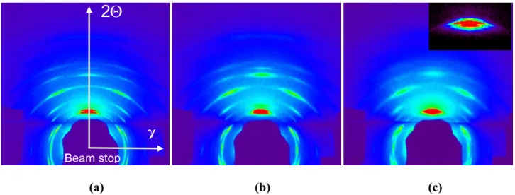
Three W/Cu multilayers deposited by magnetron sputtering have been prepared with the following period thicknesses: 9/18, 3/9 and 1.5/4.5 for W/Cu respectively. The total thickness is around 500 nm and the deposition conditions have been chosen for producing a nearly zero stress state in the film. Experiments have been performed at a photon energy of 13800 eV (λ = 0.09 nm) and a collimator of 0.1 µm. The recording time was very short thanks to the very intense x-ray beam. At first, an XRD measurement is performed on the reference sample (fig. 2) in order to calibrate precisely the geometry of the experiment i.e. the distance between the sample and the detector and also, the 3 tilt angles of the CCD. This is essential when an accuracy of 10-4 is expected on strain measurements. After a rapid comparison with a measurement in our laboratory using a standard 4-circles Seifert diffractometer working with Cu Kα, the total measurement time here is divided by a factor 3 to 4 while the number of loading steps is multiplied by a factor 2 to 3. A fabulous improvement of XRD data quality and thus strain analysis is expected. The 2D diffraction patterns obtained for the three multilayers are given fig. 3. A comment is necessary at this point to explain the feature of the image. First, the tensile set up (on both side of the 2Θ axis at the bottom) as well as the sample (horizontal dark line) “shadow” is clearly visible on the diffraction pattern. The lower part (close to the center) is obtained in transmission mode through the kapton substrate and the upper part in reflection mode. With that particular sample (metallic thin film on Kapton) and set up, it is then possible to optimize
Figure 2. 2D diffraction pattern of the LaB6 reference powder (NIST)
the measured diffraction pattern i.e. to record the maximum of information in only one pattern. In this figure 3, the contributions of tungsten and copper layers are clearly visible. Maximum intensities on the different rings indicate the presence of a fibber texture in both layers: <111> for Cu and <110> for W.
(a) (b) (c)
Figure 3: Evolution of the 2D diffraction patterns as a function of the period thickness: a) 27 nm, b) 12 nm and c) 6 nm. The effect of modulation in the growth direction is revealed for the smallest period (inset).
The contribution of both elements is always visible even though the thickness of tungsten layers is reduced down to 1.5 nm. These measurements have been done first week of February 2006. Data analysis is under progress.
Elastic properties of textured gold films
Elastic behavior of supported thin films can be then determined by combining tensile test and X-ray diffraction. Stresses applied to the films are measured as a function of intragranular strains. One advantage of this method is that no hypothesis has to be made on the residual stresses state. Indeed, some authors argued that point defects induce a triaxial residual stress state in metallic thin films that hardens the analysis. Furthermore, a pre-tensile reference state can be freely selected and thus no hypothesis has to be made on the stress-free parameter a0 of the studied thin films (which may differ from the bulk ones). The interpretation of thin film behavior encompasses the consideration of elastic grain interaction and the intrinsic structure of the films.
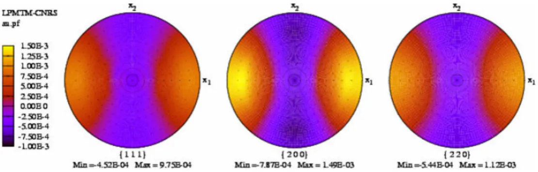
Self-consistent (SC) model, based on the extension of the Eshelby-Kröner (EK) model [8] is capable of estimating macroscopic elastic constants of a polycrystalline material considering both the ODF and the shape of the crystallites thanks to developed numerical simulations. The principle is to calculate the elastic stress and strain fields in a non-spherical ellipsoidal inclusion (grain) embedded in an elastically homogeneous matrix (polycrystal). A exemple is given fig. 4.
In-situ tensile test on gold thin films were performed on the DW22 beam line at the French synchrotron radiation facility LURE (Orsay) using a 4-circles goniometer. A wavelength (λ = 0.161 nm) was chosen to analyze five independent families of hkl planes [7]. For each experimental data point, the strain is calculated using the unloading state as a reference state. Under our experimental conditions, an increment in force ∆F = 1 N corresponds to increments in longitudinal and transversal stresses in the films of ∆σ11f = 20.5 MPa (along the deformation axis) and ∆σf22 = 5.6 MPa (perpendicular to the deformation axis) respectively. These values correspond to a ratio between transversal and longitudinal increments of approximately 27 %.
Beam stop
2Θ
The anisotropic elastic behavior of the material is revealed on a ε-sin2 Ψ plot (Ψ being the angle between the normal to the diffracting planes and the sample surface) by the non-linearity of the curves regardless of the loaded state [7] and strongly contrasts with W isotropic response. This non linearity is obtained using the developed EK model for PVD textured films. For applying the SC scheme to diffraction data, theoretical predictions need to be integrated over the diffracting volume which contains all mechanical phases satisfying the Bragg law for the actual experimental condition. The model is first applied by considering spherical Eshelby inclusions. The nonlinearity of the experimental ε-sin2 Ψ curve is then already well captured. The simulation with prolate Eshelby spheroids provides results not very different from the spherical case. Thus, as already discussed, this morphology does not allow describing the elastic behavior of the studied films even though the prolate shape apparently better approaches the columnar grain structure. Oblate shaped grains (Flat-disc) arrangement is shown to yield the best representation of the measured elastic behavior. Our results do not mean that the free surface effect is accounted for in the SC scheme, but taking the correct shape parameter for the Eshelby ellipsoid naturally reproduces a stress state compatible with the presence of a free surface.
Figure 4: Simulated strain pole figures of <111> textured gold film for a particular loading state along the x1 axis.
(a) (b) (c)
Figure 5: Evolution of the diffraction diagrams in gold film as a function of texture and film thickness: a) <111> fibber texture for a 1mm thick film, b) non textured 100nm film and c) 10 nm thick film showing a broad <111> fibber texture.
In summary, we have proposed a framework to study the anisotropic elastic properties of polycrystalline thin films in which the elastic interaction between grains, the actual structure of the film (free surface, texture) are taken into account. The approach can be extended to multiphased thin
films (multilayer, textural mixture) and does not require any assumption on the stress-free parameter and residual stress state. With the development of 2D detectors for synchrotron beam line, our proposed approach will allow great insight into film’s behavior with 2D-strain maps to be fitted to experimentally extracted ones. First measurements using 2D CCD detector have been made in February 2006 at ALS beam line 11.3.1. XRD diagrams shown in fig. 5 have been obtained with very low recording time (less than 30 seconds).
Concluding remarks
X-ray diffraction methods allow characterizing material structure and thus deformation of the unit cell resulting from residual stresses if one is able to know the unstrained unit cell or the application of external stresses. We demonstrated in this short paper that the evaluation of residual stresses using XRD and the knowledge of elastic constants is complex in thin films and can not be solved without performing appropriate mechanical testing. New possibilities at synchrotron light sources may allow in a near future 3D structural imaging thanks to sub micro focusing techniques.
Optical measurements at the sample surface using correlation methods for macroscopic strain measurements are under progress. Comparison with intra granular strains measured with x-ray diffraction will provide new insight especially grain boundaries contribution to the mechanical behavior. Another subject of interest is the simulation of elastic behavior of WCu multilayers using finite element codes widely used for plasticity and certainly adaptable for elasticity studies. This last work has been recently supported for three years by the novel French National Agency of Research which provides funding for deformation equipments and also post-doc and engineer positions. The French synchrotron radiation facility Soleil is engaged in this project as well as the LPMTM Villetaneuse (France).
References
[1] K.-F. Badawi, P. Villain, P. Goudeau, P.-O . Renault, Applied Physics Letters 80, 4705 (2002). [2] P. Villain, Ph. Goudeau, P.-O. Renault, K. F. Badawi, Applied Physics Letters 81, 23 (2002). [3] P. Villain, D. Faurie, P.-O. Renault, E. Le Bourhis, P. Goudeau, K.-F. Badawi, Mater. Res. Soc.
Symp. Proc. 875, 01.3.1 (2005)
[4] P.-O. Renault, E. Le Bourhis, P. Villain, P. Goudeau, F. Badawi, D. Faurie, Applied Physics Letters 83, 473 (2003).
[5] D. Faurie, P.-O. Renault, E. Le Bourhis, P. Villain, P. Goudeau, F. Badawi, Thin Solid Films 469-470, 201 (2004).
[6] D. Faurie, P.-O. Renault, E. Le Bourhis, P. Goudeau, Mater. Res. Soc. Symp. Proc. 875, 04.7.1 (2005)
[7] D. Faurie, P.-O. Renault, E. Le Bourhis, P. Goudeau, Journal of Applied Physics 98, 093511 (2005)..
[8] D. Faurie, P.-O. Renault, E. Le Bourhis, P. Goudeau, O. Castelnau, R. Brenner, G. Patriarche, submitted
[9] http://xraysweb.lbl.gov/BL1131/1131website/index.htm
[10] P. Villain, P. Beauchamp, K.F. Badawi, P. Goudeau *, P.-O. Renault, Scripta Materialia 50, 1247 (2004)
[11] P. Goudeau , P. Villain, T. Girardeau, P.-O. Renault, K.-F. Badawi, Scripta Materialia 50, 723 (2004).