HAL Id: cea-01615661
https://hal-cea.archives-ouvertes.fr/cea-01615661
Submitted on 12 Oct 2017
HAL is a multi-disciplinary open access
archive for the deposit and dissemination of
sci-entific research documents, whether they are
pub-lished or not. The documents may come from
teaching and research institutions in France or
abroad, or from public or private research centers.
L’archive ouverte pluridisciplinaire HAL, est
destinée au dépôt et à la diffusion de documents
scientifiques de niveau recherche, publiés ou non,
émanant des établissements d’enseignement et de
recherche français ou étrangers, des laboratoires
publics ou privés.
Influence of the substrate on the solid-state reaction of
ultra-thin Ni film with a In_0.53Ga_0.47As under-layer
by means of full 3D reciprocal space mapping
S. Zhiou, Philippe Rodriguez, Patrice Gergaud, Fabrice Nemouchi, Thanh Tra
Nguyen
To cite this version:
S. Zhiou, Philippe Rodriguez, Patrice Gergaud, Fabrice Nemouchi, Thanh Tra Nguyen. Influence of
the substrate on the solid-state reaction of ultra-thin Ni film with a In_0.53Ga_0.47As under-layer
by means of full 3D reciprocal space mapping. 2015 IEEE International Interconnect Technology
Conference and 2015 IEEE Materials for Advanced Metallization Conference (IITC/MAM), May 2015,
Grenoble, France. pp.63 - 66, �10.1109/IITC-MAM.2015.7325627�. �cea-01615661�
Influence of the substrate on the solid-state reaction
of ultra-thin Ni film with a In
0.53
Ga
0.47
As under-layer
by means of Full 3D Reciprocal Space Mapping
S. Zhiou, Ph. Rodriguez, P. Gergaud and F. Nemouchi
Univ. Grenoble Alpes, F-38000 Grenoble, France CEA, LETI, MINATEC Campus, F-38054 Grenoble, France
Email: seifeddine.zhiou@cea.fr
T. Nguyen Thanh
Univ. Grenoble Alpes, Inst NEEL, F-38042 Grenoble, France CNRS, Inst NEEL, F-38042 Grenoble, France
Abstract—We studied the solid-state reaction of Ni thin films with InGaAs layers grown on InP or Si substrates. The inter-metallics obtained carried an hexagonal structure, but yielded a difference in orientation regarding either the substrates or the annealing temperature.
I. INTRODUCTION
Among the hot topics driving the developments of new devices, the III-V materials (especially InGaAs alloys) repre-sent serious candidates to replace silicon in elaborating sub 10 nm MOSFET [1]. It was demonstrated that such components exhibit a significant raise of electron mobility throughout the channel and limit the band-to-band tunnel leakage [2]. However, for cost efficiency and manufacturability reasons, these materials must be implemented on 12 inches silicon wafers rather than conventional III-V substrates (for instance InP which diameter does not exceed 4 inches). Consequently, III-V epitaxial layer grown onto silicon wafer is part of the main challenges due to the large unit cell parameter mismatch. In parallel, several processes, such as gate stack, source and drain contacts. . . , must be taken into account and separately developed.
Thus, an ultra-low contact resistivity (10−9 Ω.cm2) is mandatory to reach entire device performances and will be therefore one of the key challenges for advanced node CMOS development. Historically, the developments of low-resistive contact have been a fine mechanism understanding in order to control the solid-state reaction (SSR) of a metal film with the Si substrate and finally the process and its related contact resistivity. There have been also intense investigations on silicide technology (e.g. TiSi2, CoSi2and NiSi) [3] over more
than 25 years, leading to fundamental understanding on the peculiar microstructure observed for these compounds obtained by SSR [4], [5]. On the contrary, the knowledge turns out to be limited when it comes to ohmic metal contacts on III-V materials for MOSFET applications. For such alloys, salicide-like technology has been recently developed and it have been found that Ni-InxGa1−xAs alloy is a promising material
for self-aligned metal source/drain (S/D) of InxGa1−xAs
n-MOSFETs [6], [7].
Thus, this paper aims to report the study carried out from the solid state reactions of Ni with InGaAs epitaxially grown on various substrates. We then focus on phase formation and
the exhibited texture of these Ni-InGaAs intermetallic layers. We finally point out the influence of InGaAs crystalline quality when directly performed on silicon wafer and refer to the layer obtained on InP.
II. EXPERIMENTAL PART
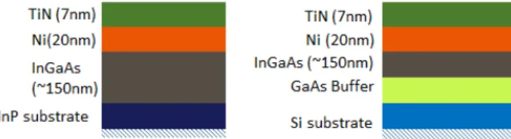
The samples were prepared by RF-PVD of Ni on In0.53Ga0.47As grown on InP or Si substrates. The metallic
layers are capped with a TiN thin film to prevent atmosphere contamination. Full description of the samples is given in figure 1. The samples were annealed at different temperatures during 60 s and under N2flow using Rapid Thermal Annealing
(typically 250 °C, 350 °C, 450 °C and 550 °C).
Fig. 1. Scheme of the as-deposited stacks of the prepared samples: (a) TiN/Ni/InGaAs/InP, (b) TiN/Ni/InGaAs/GaAs/Si.
X-ray diffraction experiments have been performed on the BM02 beamline at ESRF. They were done at an energy of 9 keV using a 6-circles goniometer. We will refer in this abstract to the χ, φ, and 2θ angles as the angles of a conventional 4-circles diffractometer. A 2D pixel detector was used to collect the diffracted beams. Such detector allows collecting data over a relatively wide range of the reciprocal space at one time and data treatment was performed with the homemade DEVA software [8]. The setup of the diffractometer and detector was such that we were capable of measuring, at a given tilt angle of the sample (φ), a range of 30° of 2θ during a one-shot-measurement. Two values of χ tilt were chosen to cover a range going from 0° to about 70° depending on the 2θ position, and multiple measure steps were added by rotating the sample around it’s normal (φ) to obtain full pole figures over 360°.
III. RESULTS
The reaction of Ni on GaAs have been described by Guivarch et al. [7], showing the formation of the intermetallic
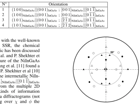
TABLE I. SUMMARY OF THE ORIENTATIONS OBSERVED FORNI/INGAAS/INPANDNI/INGAAS/SI. EACH SYMBOL CORRESPOND TO AN ORIENTATION INFIGURE3.
Symbol N° Orientation
1 (1 0 0)NiInGaAs||(0 0 1)InGaAs ; [0 0 1]NiInGaAs||[0 1 1]InGaAs
l 2 (1 0 0)NiInGaAs||(0 0 1)InGaAs ; [0 0 1]NiInGaAs||[0 1 1]InGaAs
s 3 (1 0 1)NiInGaAs||(0 0 1)InGaAs ; [2 1 2]NiInGaAs||[0 1 1]InGaAs
4 4 (1 0 1)NiInGaAs||(0 0 1)InGaAs ; [2 1 2]NiInGaAs||[0 1 1]InGaAs
with an hexagonal structure, in coherence with the well-known NiAs structure. In case of Ni/InGaAs SSR, the chemical composition and texture of the intermetallic has been discussed in only few papers. For instance, Ivana et al. and P. Shekhter et al [9], [10] describe the hexagonal structure of the NiInGaAs with the 4:1:1:2 relative composition. Zhang et al. [11] found a similar composition ratio of 51:12:14:23. P. Shekhter et al [10] also found the following orientation for the intermetallic NiIn-GaAs : (1 0 0)NiInGaAs||(0 0 1)InGaAs; [0 0 1]NiInGaAs||[0 1 1]InGaAs
(defined as orientation 1 in Table I). From the multiple 2D datasets we measured by XRD, two kinds of information have been extracted: i) De-textured 2theta diffractograms (not shown here) were obtained by summing over χ and φ the Debye rings of all the 2D snapshots; ii) pole figures (see for instance figures 3, 4 and 5) were reconstructed for several hkl reflections (or 2θ angles). From the indexation of these diffractograms and from the symmetry of the pole figures, we identified clearly the intermetallic phases that appear during SSR with an hexagonal structure. However, our results exhibit some discrepancies with the works cited previously, especially concerning the texture of the intermetallic, as shown hereafter. A. Ni on InGaAs on Si substrate
For the Ni/InGaAs/Si, no reaction occurs up to 250 °C annealing temperature. At 350 °C, the intermetallic phase is appearing and the Ni is fully consumed. This phase is still observed at 450 °C with similar pole figures at both temperatures. In agreement with the results published by P. Shekhter et al. [10] and thanks to these pole figures, we identify the occurrence of an hexagonal structure. Thus far, we identify two out-of-plane orientations of the hexagonal phase instead of one in [10] and also variants of in-plane orientations for each out-of-plane orientation instead of one compared to the previous reference. All the observed orientations of the hexagonal structure is given in Table I and a stereographic projection with the corresponding orientation for each pole is given in Figure 2.
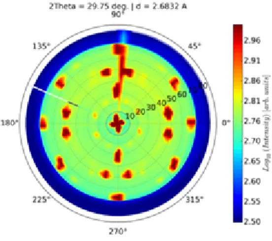
Actually, in the case of Ni deposited on InGaAs/Si we observe multiple poles for the pole figure at 2θ= 29.75° (Figure 3). Poles at χ=33° and χ=65° correspond to the projection of (1 0 1) plane of the intermetallic phase on the (1 0 0) plane along two in-plane directions (see orientation 1 and 2 in Table I) and the poles at χ=49° and χ=67° correspond to the projection of (1 0 1) on the (1 0 1) planes along two in-plane directions of the hexagonal structure (orientation 3 and 4). The fact that there are 2 sets of poles situated at χ=33° and χ=65° but at a different φ angle implies that they correspond to the same (1 0 0) orientation of the intermetallic hexagonal structure but with the existence of a second in-plane orientation along the [0 1 1] direction of InGaAs.The same goes for the out-of-plane orientations (3 and 4), where the intermetallic hexagonal structure is aligned along two equivalent directions
Fig. 2. Stereographic projection of the (1 0 1) planes of the intermetallic hexagonal structure for the different orientations given in Table I.
Fig. 3. X-ray diffraction pole figures of Ni/InGaAs/Si sample (after a 450 °C RTA annealing). The fixed 2θ angle was 29.75° corresponding to the intermetallic (1 0 1) reflection. The concentric dashed circles correspond to the χ angle landmarks with a 10° step.
[0 1 1] and [0 1 1]. In summary, for the Ni/InGaAs/Si substrates, the intermetallic shows the 4 orientations described in Table I and it keeps these orientations even at higher temperatures. B. Ni on InGaAs on InP substrate
For Ni/InGaAs/InP, the presence of such orientation was expected providing that [0 1 1] and [0 1 1] are equivalent direc-tions in the zinc blende system of InGaAs. But we observed different result (Figure 4); since only 3 orientations are iden-tified (orientation 1, 3 and 4 in Table I). The second (1 0 0) in-plane orientation did not show up during the annealing and growth of the intermetallic.
When the sample is annealed at 550 °C, further orienta-tion change occurs. The hexagonal structure loses one of its
Fig. 4. X-ray diffraction pole figures of Ni/InGaAs/InP sample (after a 450 °C RTA annealing). The fixed 2θ angle was 29.75° corresponding to the intermetallic (1 0 1) reflection. The concentric dashed circles correspond to the χ angle landmarks with a 10° step.
out-of-plane orientations (orientation 1) and another in-plane orientation (orientation 4). Thus, the so-formed intermetallic yields only one orientation at 550 °C which is orientation 3 (Figure 5).
Fig. 5. X-ray diffraction pole figures of Ni/InGaAs/InP sample (after a 550 °C RTA annealing). The fixed 2θ angle was 29.75° corresponding to the intermetallic (1 0 1) reflection. The concentric dashed circles correspond to the χ angle landmarks with a 10° step.
IV. DISCUSSION
We demonstrate that the intermetallic obtained by SSR of a Ni layer with a InGaAs/InP substrate exhibits an hexagonal structures with two out-of-plane orientations. Yet, there are two equivalent directions along InGaAs,[0 1 1] and [0 1 1]. These directions are thermodynamically equivalent, so it is expected that the intermetallic would grow along these two directions, which is not the case as no corresponding poles appear on the pole figure. Further, we demonstrated that the intermetallic formed on InGaAs/Si yields the four orientations along in-plane and out-of-in-plane directions. This particular evolution of the pole figure may be explained as the following : the InP substrates might yield a low angle miscut that prevents (1 0 0) planes from being completely parallel to the sample. Thus the
substrate, and the deposited InGaAs layer, loose their four-fold symmetry and may lead to the formation of the intermetallic along some preferred directions that could be explained by epitaxial or axiotaxial relationship [5] . This point will need to be further discussed.
V. CONCLUSION
We have observed that the Ni-InGaAs intermetallic com-pound can yield multiple orientations in-plane and out-of-the-plane. These orientations depend not only on the substrate but also on the temperature of annealing (e.g. intermetallic agglomeration, etc.). Such difference of orientations may have impact on the electrical properties of these compounds. Other investigations concerning X-Ray Diffraction in-situ studies of the intermetallic and chemical composition determination using Atomic Probe Tomography are currently under progress along with a novel study on another intermetallic compound formed by SSR of Ni-based-alloy on InGaAs.
AKNOWLEDGMENTS
This work has been supported by the LabEx Minos ANR-10-LABX-55-01 and funded by the French National Research Agency (ANR) under the “Investissements d’avenir” program (2 projects with the grant numbers: ANR-11-EQPX-0010 and FDSOI11). The authors would also thank the BM02-D2AM French CRG Beamline’s staff at ESRF for their collaboration and Thierry Baron from CNRS-LTM for the InGaAs epitaxy.
REFERENCES
[1] “International Technology Roadmap for Semiconductors,” 2013. [2] J. A. del Alamo, “Nanometre-scale electronics with III-V compound
semiconductors,” Nature, vol. 479, no. 7373, pp. 317–323, Nov. 2011. [3] H. Iwai, “Roadmap for 22nm and beyond (Invited Paper),”
Microelec-tronic Engineering, vol. 86, no. 79, pp. 1520 – 1528, 2009.
[4] S. Gaudet, K. De Keyser, S. Lambert-Milot, J. Jordan-Sweet, C. De-tavernier, C. Lavoie, and P. Desjardins, “Three dimensional reciprocal space measurement by x-ray diffraction using linear and area detectors: Applications to texture and defects determination in oriented thin films and nanoprecipitates,” J. Vac. Sci. Technol., A, vol. 31, no. 2, p. 021505, 2013.
[5] C. Detavernier, A. S. ¨Ozcan, J. Jordan-Sweet, E. A. Stach, J. Tersoff, F. M. Ross, and C. Lavoie, “An off-normal fibre-like texture in thin films on single-crystal substrates,” Nature, vol. 426, pp. 641–645, 2003. [6] X. Zhang, H. Guo, H.-C. Chin, X. Gong, P. S. Y. Lim, and Y.-C.
Yeo, “Self-Aligned NiGeSi Contacts on Gallium Arsenide for III-V MOSFETs,” ECS Trans., vol. 33, no. 6, pp. 1021–1028, 2010. [7] A. Guivarc’h, R. Gu´erin, J. Caulet, A. Poudoulec, and J. Fontenille,
“Metallurgical study of Ni/GaAs contacts. II. Interfacial reactions of Ni thin films on (111) and (001) GaAs,” J. Appl. Phys., vol. 66, no. 5, pp. 2129–2136, 1989.
[8] T. N. Thanh, E. Bourjot, S. Zhiou, V. Kovacova, P. Rodriguez, F. Nemouchi, N. Blanc, N. Boudet, and P. Gergaud, “Full 3D Reciprocal Space Map of thin polycrystalline films for microelectronic applica-tions,” IITC/MAM Conference Proceedings, 2015, to be published. [9] Ivana, Y. Lim Foo, X. Zhang, Q. Zhou, J. Pan, E. Kong, M. H.
Samuel Owen, and Y.-C. Yeo, “Crystal structure and epitaxial relation-ship of Ni4InGaAs2 films formed on InGaAs by annealing,” J. Vac. Sci. Technol., B, vol. 31, p. 012202, 2013.
[10] P. Shekhter, S. Mehari, D. Ritter, and M. Eizenberg, “Epitaxial NiIn-GaAs formed by solid state reaction on In0.53Ga0.47As: Structural and chemical study,” J. Vac. Sci. Technol., B, vol. 31, no. 3, p. 031205, 2013. [11] X. Zhang, Ivana, H. X. Guo, X. Gong, Q. Zhou, and Y.-C. Yeo, “A Self-Aligned Ni-InGaAs Contact Technology for InGaAs Channel n-MOSFETs,” J. Electrochem. Soc., vol. 159, no. 5, pp. H511–H515, 2012.