Section 1
Computer-Aided
Design
Section
2 Digital Signal Processing
Sectio 1 CoputerAidedDesig
Chaptr 1 Cstom
ntegrted Crcuit
Chpe 2Cmutr
ntgae Dsg adMnuatr
of Integraed Circuit
Chapter 1. Custom Integrated Circuits
Chapter 1. Custom Integrated Circuits
Academic and Research Staff
Professor Jonathan Allen, Professor John L. Wyatt, Jr., Professor Srinivas Devadas, Professor Anantha P. Chandrakasan, Professor Jacob K. White, Professor Berthold K.P. Horn, Professor Hae-Seung Lee, Pro-fessor Martin A. Schmidt, ProPro-fessor Stephen D. Senturia, ProPro-fessor Chales G. Sodini, Dr. Robert C. Armstrong, Dr. Donald G. Baltus, Dr. Scott B. Dynes, Dr. Ichiro Masaki
Visiting Scientists and Research Affiliates
Daniel W. Engels, Dr. Andrew Lumsdaine,1 Mark W. Reichelt,2 Dr. Herre S.J. van der Zant
Graduate Students
Narayana R. Aluru, Jason R. Bergendahl, Michael T. Chou, Geoffrey J. Coram, Steven J. Decker, Michael S.
Ehrlich, Ibrahim M. Elfadel, Farzan Fallah, Jeffrey C. Gealow, George I. Hadjiyiannis, Silvina Z. Hanono,
Mattan Kamon, Stan Y. Liao, Robert G. McDonald, David R. Martin, Yehia M. Massoud, Ignacio S. McQuirk,
Jos6 C. Monteiro, Keith S. Nabors, Ognen J. Nastov, Joel R. Phillips, Khalid Rahmat,3 Chin Hwee Tan, Johannes Tausch, Paul C. Yu
Technical and Support Staff Susan E. Chafe, Dorothy A. Fleischer
1.1 Custom
Integrated
Circuit Design
Sponsors
IBM Corporation
MIT School of Engineering
Project Staff
Professor Jonathan Allen, Dr. Robert C. Armstrong, Dr. Donald G. Baltus, Dr. Scott B. Dynes, Michael S. Ehrlich, Robert G. McDonald, Chin Hwee Tan The goal of this group includes the study of performance-directed synthesis of custom VLSI cir-cuits. Nineteen-ninety-five was a transition year as many group members finished their projects and left MIT. Dr. Donald Baltus completed his doctoral dis-sertation on the design of systolic arrays.4 His
dis-sertation was one of two selected by MIT for submission to the annual ACM thesis prize competi-tion, a significant recognition and honor. Chin Hwee Tan completed her SM thesis on transistor sizing for power minimization under a delay constraint5 and presented her research at the annual Work-shop on Low-Power Design.6 Dr. Robert Armstrong completed his postdoctoral study on further refine-ment to the FICOM consistency maintenance CAD environment. Finally, Robert McDonald, who was developing a CAD system for the design of self-resetting CMOS circuits, has left MIT to apply these techniques in industry.
The major continuing effort has been the design and implementation of an interactive learning envi-ronment for VLSI design. There are two major components of this research. First, most of a major text has been developed for and utilized in MIT
1 Notre Dame University, Notre Dame, Indiana.
2 Mathworks, Natick, Massachusetts.
3 Hewlett-Packard Corporation.
4 D.G. Baltus, Efficient Exploration of Affine Space-Time Transformations for Optimal Systolic Array Synthesis, Ph.D. diss., Dept. of Electr. Eng. and Comput. Sci., MIT, 1994.
5 C.H. Tan, Optimization of Power and Delay in VLSI Circuits Using Transistor Sizing and Input Order, S.M. thesis, Dept. of Electr.
Eng. and Comput. Sci., MIT, 1994.
6 C.H. Tan and J. Allen, "Minimization of Power in VLSI Circuits Using Transistor Input Ordering and Statistical Power Estimation," paper presented at the International Workshop on Low-Power Design, Napa, California, April 24-27, 1994.
Chapter 1. Custom Integrated Circuits
subject 6.371 (Introduction to VLSI Systems) by Professor Jonathan Allen. This text, with its accom-panying illustrations, has been well received for two semesters, and it continues to be extended and refined. The text will be converted to hypertext, and the figures will be realized in several formats. Simple illustrations, including photographs and graphs, will be digitized and represented as static figures. In addition, circuit schematics and layout will be represented in a CAD system environment so that users (students) can directly explore the behavior of the circuit. Thus, for example, when a student encounters a schematic diagram of a circuit in hypertext, control can be shifted directly to a circuit schematic editor.
In this environment, various input signals can be applied to the circuit, and results obtained imme-diately from a simulator with appropriate viewing software. In addition, the circuit schematic can be edited by the student (for example, transistor sizes can be modified), and the behavior of the resulting circuit studied and compared to other versions. It is believed that this ability to experiment directly with circuits is central to developing an understanding of large-voltage-swing (nonlinear) digital circuits. Tight coupling between the hypertext and the CAD system is central to the goals of this project.
Considerable effort has been devoted to the selection of an appropriate CAD environment. It must be small, fast, and inexpensive, yet with
suffi-cient capability to serve the needs within this inter-active learning environment. Both schematic and layout editors are required, and a circuit extraction (from layout) program is needed. A circuit simulator with viewing routines is also needed along with appropriate input-output interfaces.
For these requirements, the large, well-known CAD systems are inappropriate, and so significant effort was devoted to develop the FICOM design editing system, which was developed by Dr. Robert Armstrong to a point where it could be incorporated into the overall interactive learning environment system. Unfortunately, this effort was not suc-cessful. Attention is now focused on the use of a small, commercially available CAD system that can be readily learned and easily controlled from the hypertext. Experiments with a candidate system are now underway, and methods to couple the hypertext and CAD systems are under study. Dr. Scott Dynes, who has extensive multimedia design and programming experience, has joined the project as a postdoctoral associate. Graduate student Michael Ehrlich is contributing to the design of the system from a user perspective. Plans are to have an initial prototype of the system running by the fall of 1996, so that user feedback can be solicited and guidance for further development can be obtained.
1.2 Cost-Effective Hybrid Vision
Systems for Intelligent Highway
Applications
Sponsor
National Science Foundation Grant MIP 94-23221
Project Staff
Professor Berthold K.P. Horn, Professor Hae-Seung Lee, Dr. Ichiro Masaki, Professor Martin A. Schmidt, Professor Charles G. Sodini, Professor John L. Wyatt, Jr., Jason R. Bergendahl, Geoffrey J. Coram, Steven J. Decker, Jeffrey C. Gealow, David R. Martin, Ignacio S. McQuirk, Paul C. Yu
1.2.1 Project Summary
The cost of machine vision systems is limiting their application. The goal of this project is to develop new cost-effective architectures for vision systems and to evaluate them for intelligent highway applica-tions. We propose an advanced modular architec-ture as a way of improving the cost and performance of vision systems. We call this archi-tecture the heterogeneous nanocomputer network because it consists of variety of functional modules. Some modules are application-specific integrated circuits (ASIC) chips for straight-forward early-vision processing while the others are highly program-mable. The modules can be either analog, digital, or mixed signal. Examples of other modules include focal plane processors with visible light and an infrared imager. The heterogeneity provides a sig-nificant opportunity to lower the cost of each module by tailoring its architecture to a particular function with minimum constraints. Each functional module is called a nanocomputer because its com-putational silicon area is significantly smaller then a conventional microcomputer. Reducing module size is important for reducing total system cost. A small-grain architecture also provides greater flexibility for integrating modules. A network architecture is essential for integrating multiple modules without communication bottlenecks.
The next section details substantial progress on nine subprojects. Two image acquisition chips are under development: one for visible and the other for infrared lights. Please refer to sections 1.2.2 and 1.2.8 for more details. Two analog VLSI chips have both image acquisition and image processing func-tions (secfunc-tions 1.2.4 and 1.2.10). We are devel-oping two image processor chips (sections 1.2.3 and 1.2.5). An analog-to-digital conversion chip was
Chapter 1. Custom Integrated Circuits
also developed (section 1.2.6). Two other projects are related to automotive applications and noise models for solid-state devices, respectively (sections 1.2.7 and 1.2.10).
1.2.2 Brightness Adaptive Imager with Analog and Digital Output
Graduate student Steven Decker, working with Pro-fessor Sodini, has been designing an imager to act as the front end of a modular vision system. The imager was originally designed with a 64 x 64 pixel array of pixels in a 1.75 pm CCD/CMOS tech-nology, which was later expanded to a 256 x 256 array in a 0.8 pm CMOS process. Other features of the imaging chip include large fill factor, operating speed on the order of 1000 frames/sec, column parallel output, brightness adaptation capability, and 10-bit digital output. Static chip power at 1000 frames/second is estimated to be about 370 mW, 90 percent of which is dissipated by the on-chip A/D converters.
CCD and CMOS implementations of the wide dynamic range imager were compared, and the results presented at the 1995 IEEE Workshop on Charge-Coupled Devices and Advanced Image Sensors. It was concluded that the CMOS implemetation had no significant disadvantages and would tend to have lower smear levels than a CCD implementation. Since commercially available CMOS processes have finer linewidths than avail-able CCD/CMOS processes, a denser array is pos-sible in the CMOS process.
A 256 x 256 CMOS imager was designed, layed out, and fabricated in the HP 0.8 pm process. Four issues were addressed in the design of the CMOS imager: pixel design, generation of the lateral over-flow gate waveform, reduction of fixed-pattern noise, and analog-to-digital conversion.
A board was designed and constructed to test for basic functionality of the imager chip. The board allows the output from any single pixel in the array to be examined under realistic operating conditions. A different board will be required later to read data from the entire array.
An analysis of the sensitivity of the brightness adaptive algorithm was performed with Professor Wyatt. The goal of the analysis was to determine how much various mismatch sources in the pixel contribute to a mismatch in the voltage output from the pixel, given a desired compression ratio. Another goal was the determination of optimal barrier waveforms to minimize the effect of the mis-match terms. It was found that timing errors present a particularly important hazard. A separate analysis
was undertaken to determine the expected mis-match in CMOS pixels generally and find the extent to which correlated double sampling can compen-sate for them.
1.2.3 Analog versus Digital Approaches to
Machine Vision Hardware
Graduate student David Martin, under the super-vision of Professor Hae-Seung Lee, graduate student Steven Decker under the supervision of Professor Charles Sodini, and Dr. Ichiro Masaki are developing a stereo vision system in collaboration with Professors John Wyatt, Berthold Horn, and Jacob White. The goals of this project are twofold: (1) comparison of analog versus digital approaches, and (2) development of a practical stereo distance measurement system.
A case study to compare analog versus digital approaches is important in identifying what kinds of processing are suitable for analog implementation. An array processing function was chosen as the case for the comparison. The level of this function-definition is high enough for the generality of the result; and, at the same time, it is low enough to make the result independent from the algorithm. A hybrid analog/digital array processor chip is being developed as an example of the analog implemen-tation. It will consist of an array of mixed signal
processing elements which will work in an multi-instruction multidata (MIND) scheme. Each pro-cessing element will include a digital memory unit which will control an analog arithmetic unit and a data flow network.
processors, for this schemes such as a architecture. With thi element is assigned processing elements multiple-data (SIMD)
Examples of the digital array comparison, include various pixel-parallel array processor
is scheme, a digital processing for each pixel, and multiple work in a single-instruction fashion.
In
the first step, the vision algorithms that will run
on the array processor were simulated to determine
their accuracy and speed requirements. These
sim-ulations revealed that the algorithms could tolerate
random errors of up to 10 percent as long as no
information was lost from arithmetic overflow. In the
second step, key circuits were designed, simulated,
fabricated, and tested. As a result of these tests, it
was determined that conventional analog circuits for
arithmetic were too large and inaccurate for a
general purpose arithmetic unit. Therefore, a novel
analog arithmetic circuit was designed, simulated,
and sent to MOSIS for fabrication. This new circuit
essentially performs an A/D on a voltage and then
immediately performs a D/A on the digital value.
The output voltage is equal to the product of the
Chapter 1. Custom Integrated Circuits
input voltage and the D/A reference voltage divided by the A/D reference voltage. Setting the reference voltages correctly allows the circuit to perform multi-plication, division, addition, and subtraction.
The final processor cell is about 700 microns by 270 microns using Hewlitt-Packard's 0.8 pm triple metal process. Simulations indicate that it can operate at about two million instructions per second and consumes about 2 mW of power at this speed. Two test chips have been fabricated through MOSIS and are now being tested. One test chip has a single processing cell, the other a 5 x 5 array.
1.2.4 A BiCMOS/CCD Focus-of-Expansion Chip for Estimating Camera Motion
Graduate student Ignacio McQuirk, working with Professors Berthold Horn and Hae-Seung Lee, has continued testing the real-time analog VLSI chip he designed for determining the direction of camera motion from time-varying image sequences. The approach assumes the presence of a camera moving through a fixed world with translational vel-ocity. There is no restriction on the shape of the surfaces in the environment, only an assumption that the imaged surfaces have some texture, that is, spatial variations in reflectance. It is also assumed that the camera is stabilized so that there is no rotational motion. The focus of expansion (FOE) is the projection of the camera translation vector onto the image plane and gives the direction of camera. This location is the image point towards which the camera is moving and other image points appear to be expanding outward from.
The algorithm we use for estimating the FOE mini-mizes the sum of squares of the differences at every picture cell between the observed time vari-ation of brightness and the predicted varivari-ation given the assumed position of the FOE. This minimization is not straightforward because the relationship between the brightness derivatives depends on the distance to the surface being imaged and that dis-tance is not only unknown, but varies from picture cell to picture cell. However, image points where brightness is instantaneously constant play a critical role. Ideally, the FOE would be at the intersection of the tangents to the iso-brightness contours at these stationary points. In practice, image bright-ness derivatives are hard to estimate accurately given that the image itself is quite noisy. Hence the intersections of tangents from different stationary points may be quite scattered. Reliable results can nevertheless be obtained if the image contains many stationary points and the point is found that has the least weighted sum of squares of
perpen-dicular distances from the tangents at the stationary points. The chip itself calculates the gradient of this minimization sum, and the actual FOE estimation is performed by closing a feedback loop around it. The FOE chip has been implemented using an
embedded CCD imager for image
acquistion/storage and a row-parallel processing. A 64 x 64 version was fabricated through MOSIS in a
2 pm BiCMOS/CCD process with a design goal of 100 mW of on-chip power and a top frame rate of 1000 frames/second. Further algorithmic work also continues with Professor Wyatt to examine more robust, but more complex, algorithms which may also be suitable for implementation in analog VLSI. A complete test setup for the chip was constructed. Current testing has moved into its final phase: examining the processed output of the FOE chip and using it in a closed loop manner to estimate the FOE in real time.
1.2.5 Integrated Computing Structure for Pixel-Parallel Image Processing
Graduate student Ignacio McQuirk, working with Professors Berthold Horn, and Jeffrey Gealow, working with Professor Sodini, have been devel-oping an dense integrated processing element array to perform low-level real-time image processing tasks in the desktop computer environment. The layout pitch of one-bit-wide processing element logic is matched to the pitch of memory cells, maxi-mizing the bandwidth between memory and logic and minimizing processing element area.
A two-dimensional network connects the processing elements. Control and data paths are distinct. The processing element array receives instructions from the controller, which is managed by the host com-puter. Analog images from a video camera or other source are converted to digital signals, then refor-matted for processing using the processing element array. Output images from the array are converted to a format appropriate for subsequent use. Pro-cessing element logic is integrated with 128-bit DRAM columns in place of DRAM column decode logic.
To demonstrate the capability of the processing element array, execution of several low-level image processing tasks has been simulated. One of the investigated tasks is median filtering. The value of each output pixel is the median of all input values in a region centered at the output pixel. Median fil-tering eliminates spikes while maintaining sharp edges and preserving monotonic variations in pixel values. Operating at 10 MHz, the processing element array would perform a true 5 x 5 median filtering operation in less than 1 ms.
Chapter 1. Custom Integrated Circuits
Circuit design and layout of the core processing element array has been completed. A compact logic implementation has been developed meeting the tight layout constraints imposed by pitch-matching memory and logic. Logic circuits operate with a low-voltage supply (2.5 V), minimizing power dissipation.
A completed integrated circuit design will soon be submitted for fabrication through MOSIS. A single device will provide a 64 x 64 block of processing elements. Expected typical power dissipation is 250 mW. Packaged chips will be used to build a complete image processing system. Sixteen chips may be employed to handle 256 x 256 images.
1.2.6 A Pipelined CMOS Analog-to-digital Conversion
Graduate student Paul Yu, working with Professor Hae-Seung Lee, has been working on various tech-niques of achieving low-power video-rate analog-to-digital conversion (ADC) using CMOS technology. A 2.5-V 12-b 5-MSample/s CMOS pipelined ADC is used as a vehicle to demonstrate efficient methods of power minimization for analog systems without sacrificing performance. One of the main power minimization techniques is a commutated feedback capacitor switching (CFCS) scheme that achieves
12-b resolution while using only 6-7 b accurate
capacitor matching.
In a wide range of imaging applications, high-resolution, but medium accuracy are required. This requirement is due to the fact that human eyes, while sensitive to the difference in intensities between adjacent pixels, are quite insensitive to the absolute individual pixel intensities. Exploiting this relaxed requirement on absolute accuracy, an ADC with 12-b differential nonlinearity (DNL), only needs to have about 6-8 b of integral nonlinearity (INL). Similarly, signal-to-noise ratio (SNR), as opposed to signal-to-noise-and-distortion (SNDR) will be the primary target.
Fabricated in a 1.2 pm, double poly, double metal process in August 1994, the test chip was charac-terized from September 1994 to October 1995. We used a variety of characterization techniques including histogram and fast Fourier transform (FFT) tests. Maximum differential nonlinearity
(DNL) of +0.63/-0.78 LSB at 5 MSample/s have
been obtained. In July 1995, the conversion rate was pushed from 1 MHz to 5 MHz using reduced output swing logic. In August 1995, a discrete LC filter was designed and constructed to obtain a clean 2.2-MHz sine wave from an RF frequency synthesizer for FFT testing. At this near-Nyquist input frequency, a peak signal-to-noise ratio (SNR)
of 67.6 dB was obtained. The single-ended input capacitance of the ADC is only 1.0 pF. This is sig-nificantly lower than many previously reported video rate ADCs, especially those using the flash archi-tecture.
1.2.7 Real-time Vision System for Automotive Applications
Graduate student Jason Bergendahl, under the supervision of Professor Berthold Horn and Dr. Ichiro Masaki, is developing a real-time machine vision system for stereo distance measurements in automotive applications. The basic approach differs substantially from those used by other stereo vision systems under development. First, the stereo dis-tance measurements will rely on edge correlation between stereo pairs, instead of area correlation. The algorithm is greatly simplified to allow real-time performance at frame rate (30 frames/second) to be realized. Another important difference is that the distance measurements are based on sub-pixel dis-parity measurements between the stereo pairs, allowing for a compact camera arrangement that does not preclude accurate distance measurement. The system, consisting of three miniature cameras and supporting image processing hardware, will be installed in a test vehicle for on-road trials. Thus, we will be able to directly evaluate the feasibility of vision-based adaptive cruise control under realistic highway conditions. We can also make meaningful performance comparisons between vision-based methods and millimeter wave radar approaches. Our goal is to demonstrate a stereo vision system with performance equal to that of millimeter-wave radar. However, unlike radar systems, a vision-based system may be expanded to provide addi-tional funcaddi-tionality, such as as lane tracking. To meet the computational demands of real-time machine vision at frame rate, commercially avail-able image processing hardware and personal com-puters are used in our system.
The first phase of the project consisted of a thor-ough evaluation of candidate host systems to oversee the image acquisition and processing tasks. Desktop PCs, "luggable" PCs, laptop PCs, workstations, and VME systems were considered. The primary concern was availability of off-the-shelf plug-in hardware; however each candidate system was also evaluated for processing power, bus bandwidth, and portability. A Pentium-based desktop PC with PCI bus was selected to serve as the host system. This host's key advantage is the high sustainable data transfer rates (up to 133 MBytes/sec) between bus mastering PCI cards and the host.
Chapter 1. Custom Integrated Circuits
In parallel with host selection, software develop-ment of simple stereo vision algorithms was begun. The objective was twofold: (1) to evaluate the per-formance of candidate algorithms, and (2) to esti-mate the capabilities of a workstation or PC for performing image processing without the aid of additional hardware. One software implementation of a simplified algorithm, performed by Gideon Stein, realized 6 Hz performance on a Silicon Graphics workstation. This result suggests that while image processing software is a useful tool for algorithm development, real-time performance with our algorithms requires that most computationally intensive image processing tasks be performed in hardware.
1.2.8 Uncooled Infrared Imager
The micromachined, uncooled infrared detector design which we are investigating consists of a thermally-isolated silicon island containing a bipolar transistor configured as a temperature sensing diode. The island is thermally isolated by sus-pending it several microns above the silicon chip surface and supporting it with thin silicon nitride tethers. A process technology is used which facili-tates integration of electronics in the region sur-rounding the pixels. This technology employs silicon wafer bonding and has previously been demon-strated on micromachined pressure sensors and accelerometers.
A model to predict the sensitivity and noise of a single pixel has been developed utilizing standard lumped parameter thermal models and first order models for the temperature sensitivity of diodes. Using these models and some target performance specifications, a set of geometric parameters were determined. In some instances, the geometry had additional constraints imposed by the practical limi-tations of the technology. In particular, the minimum dimension of the pixel element is 5 micron, which was a conservative limitation imposed by the several micron step heights between the silicon island and the nitride tethers. While the current geometry is chosen to be conservative, more aggressive geometry can be attempted after the first prototype is fabricated and the limitations of the technology are understood. The total pixel size is
140 micron by 140 micron. The silicon nitride membrane is 1 micron thick, and the silicon island which contains the diode is 3 microns thick. The thermal conductivity is strongly influenced by the interconnect metal, which is made as thin as pos-sible to reduce the conductivity. There is a trade-off against the increase in interconnect resistance, which impacts noise. The metal thickness was chosen to be 0.1 micron.
The process technology development plan we are pursuing involves several steps and leverages off previous technology which we have developed for integrated sensors. The process enhancements which are needed for the infrared detector are: silicon nitride membranes; diode processing on silicon islands; and metalization on the nitride and silicon island. The first step is to demonstrate the integrity of the nitride membranes through high tem-perature processes. The next step is to develop the metalization process with the required step cov-erage. The final step in process development will be the actual fabrication of the pixel elements.
1.2.9 Physically Correct Noise Models for Solid-State Devices
Noise imposes a fundamental limit to analog cir-cuits, especially in low-power operation. Under the direction of Professor Wyatt, graduate student Geoffrey Coram has been studying nonlinear device noise models for agreement with fundamental phys-ical theory. Accepted models for noise in nonlinear devices do not agree with thermodynamic princi-ples. Mr. Coram is looking to resolve this discrep-ancy while maintaining consistency with experimental results.
In general, continuous-time Gaussian white noise is nonphysical, since it has an infinite variance. Poisson (i.e., shot noise) models give a more phys-ical basis for accurate models. Probability theory tells us that Poisson processes can become Gaussian in the limit of numerous small jumps, and it is possible to derive Nyquist-Johnson thermal noise (4 kTR) as the limit of a Poisson-noise system.
We have recently shown that no Gaussian white-noise model can be physically correct for nonlinear devices-all such models predict circuit behavoir that is contrary to thermodynamic principles. More importantly, we have also found a Poisson process model that agrees with thermodynamic theory. It accurately describes noise behavoir of the pn junc-tion and the subthreshold MOSFET at arbitrary bias points. Using the requirements of a Maxwell-Boltzmann equilibrium distribution and conformance with the Second Law of Thermodynamics, one can calculate the rates of the Poisson sources solely from the constitutive (current-voltage) relation for the device. This sort of nonlinear fluctuation-dissipation relation has been long sought in the lit-erature.
This model accurately decribes devices where the current results solely from thermal fluctuations over a barrier and/or from diffusion. It also fits the linear
Chapter 1. Custom Integrated Circuits
resistor, with a pure drift transport mechanism. Pro-fessor Wyatt and Mr. Coram are now attempting to extend the model to the more general class of devices with both drift and diffusion.
1.2.10 Time-to-Collision Warning Chip
Under certain circumstances, it is possible to esti-mate the time-to-collision (TTC) from a time varying image. It would be useful to encapsulate an algo-rithm for doing this into a cheap camera, ideally with computation done on the chip that senses the image, or at least within the enclosure of the camera box itself. In this way, there is no need to move large volumes of image data from an image sensor to an image processor.Such a device performs an extreme bandwidth compression: it has high bandwidth in (image sequence) and low bandwidth out (time-to-collision). This device could be outfitted with a cheap plastic lens and used as a warning system, aimed out the rear of a car into the two "blind spots" not easily visible in a driver's mirrors.
The key to recovering the time-to-collision is the realization that there are constraints between the brightness gradient (spatial derivatives of bright-ness) and the time derivative of brightness at a point in the image. These depend on the motion field, and the motion field in turn depends on the rigid body motion between the camera and the object being viewed.
We have formulated the problem using the (1) per-spective projection equation, (2) motion field equa-tion, and (3) constant brightness assumption. This leads to equations relating camera motion and image brightness gradients.
We have developed a least squares formulation that involves minimizing the sum of a set of error terms. The error terms are simply the differences between observed rates of change of brightness and predicted rates of change, based on the motion parameters and the scene description. The least squares problem does yield to a closed form sol-ution, but this involves eigenvectors and eigen-values. While these can be computed in digital or
analog hardware, it is a difficult task.
Instead, we are now exploring an iterative method that alternately solves for the surface normal of the plane used to approximate the scene and the translational motion vector. This will be much easier to implement in either digital or analog hard-ware. We expect it to be fast enough despite the iterative nature of this method.
We will first explore a number of algorithmic alter-natives on existing work stations using both real image sequences created under controlled condi-tions as well as synthetic sequences where the
motion and shapes of objects are known exactly.
1.3 Computer-Aided Design Techniques
for Embedded System Design
Sponsor
Defense Advanced Research Projects Agency/
U.S. Army Intelligence Center
Contract DABT63-94-C-0053
Project Staff
Professor Srinivas Devadas, George I. Hadjiyiannis, Silvina Z. Hanono, Stan Y. Liao, Daniel W. Engels
1.3.1 Embedded Systems and
Hardware/Software Codesign
One of the challenges of micro-architectural design is to harness the capabilities supplied by improved semiconductor processing. The advent of submicron processing allows for the integration of
5-10 million transistors on a single integrated-circuit (IC). One micro-architecture that effectively exploits
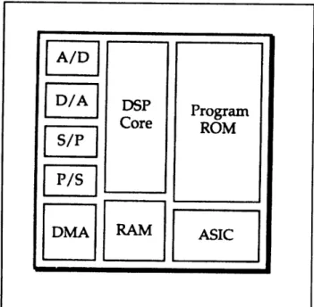
the capability of the silicon integrates a micro-processor, digital-signal processor (DSP) or a
micro-controller, with a ROM and an ASIC all in a single IC (figure 1). Micro-architectures of this style can currently be found in such diverse embedded systems as FAX modems, laser printers, and cel-lular telephones. To justify the design costs of such a product, as well as the utilization of such a level of integration, these embedded system designs must be sold in very large numbers and as a result, they are also very cost sensitive. The cost of the
IC is most closely linked to the size of the IC, and
that is derived from the final circuit area. It is not unusual for the single largest factor in the area of such ICs to be the ROM storing the program code for the microprocessor. In these embedded systems, the incremental value of using logic opti-mization to reduce the size of the ASIC is smaller because the ASIC circuitry is a relatively smaller percentage of the final circuit area. On the other hand, the potential for cost reduction through dimin-ishing the size of the program ROM is great. There are also often strong real-time performance require-ments on the final code, so there is a necessity for producing high-performance code as well.
Chapter 1. Custom Integrated Circuits
DSP
Program
A/D
D/
DSP
Program
Core
ROM
i
I
F
P/S
DMA
RAM
ASIC
I
I
_ _ _
Figure 1. A typical embedded sytem.
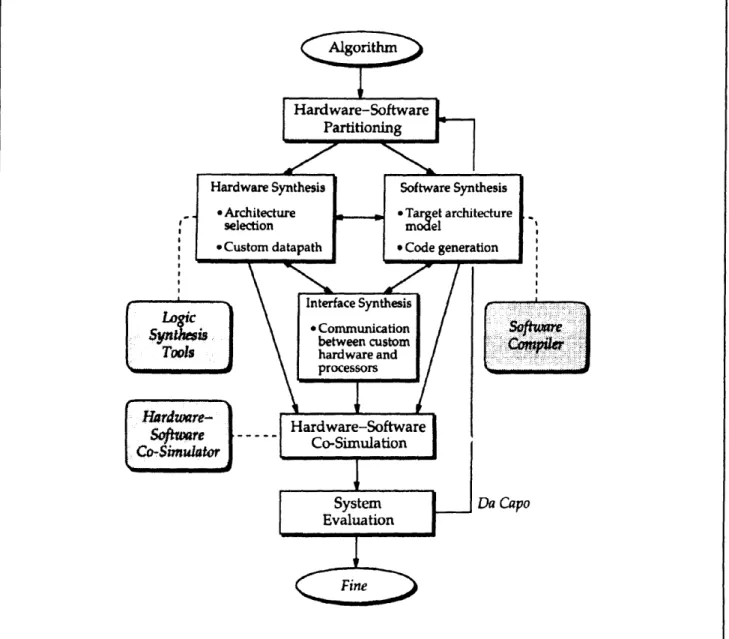
In a hardware/software codesign flow for such an embedded system, the designer first determines which parts of the functionality of the system will be implemented in hardware and which parts in soft-ware. The designer then proceeds to design each of the hardware and software components. The system is simulated and evaluated with a hardware-software co-simulator. If the results of the simu-lation meet design specifications (e.g., correctness and timing constraints), then the design is accepted. Otherwise, the designer may re-partition the original algorithmic specification and iterate the same process. This is illustrated in figure 2.
Under this methodology, tools for code generation and hardware-software co-simulation are essential items in the designer's tool-box. Specifically, com-pilers for software written in high-level languages are indispensable in the design of embedded systems.
1.3.2 Reducing Code Size
A given target die size for an embedded system
product may limit the size of the ROMs and there-fore the size of the code. In many embedded system projects, the ROM space estimated at the beginning becomes insufficient later in the develop-ment phase or during maintenance. Designers usually have to work diligently to reduce the code size in order to avoid excessive design modification.
The traditional approach to these problems has been to write the embedded code in assembly lan-guage. As the complexity of embedded systems grows, programming in assembly language and optimization by hand are no longer practical or eco-nomical, except for time-critical portions of the program that absolutely require it. Recent statistics from Dataquest indicate that high-level languages
(HLLs) such as C (and C++) are definitely replacing assembly language, because using HLLs greatly lowers the cost and time of development, as well as the maintenance costs of embedded systems. However, programming in a HLL can incur a code size penalty.
There are a number of reasons for this. One reason is that compiler optimization techniques have classically focused on code speed and not code density. Also, most available compilers opti-mize primarily for speed of execution. Although some optimizing transforms such as common sub-expression elimination can improve both speed and size at the same time, in many cases there is a speed-size trade-off. For example, subroutine calls take less space than in-line code, but are generally slower. Where execution speed is not critical, mini-mizing the code size is usually profitable. A second reason is that compiler-optimization techniques have typically been limited to approaches which can be executed quickly [ s O(n)] because programmers require fast compilation times during development. For this reason the numerous NP-hard optimization problems associated with code optimization are rarely faced directly, as in computer-aided design, but are usually approached with simple linear-time heuristics.
Thus a central theme of our embedded system design project is that a new goal for code-optimization has emerged: The generation of the most dense code obtainable with the highest performance-within any reasonable compilation time. We have two important premises. First, the methodology required to generate this code will be most useful if it is retargetable-it can be easily changed to generate code for many different processors. Second, the methodology will require-in addition to traditional code optimizations-techniques analogous to the meth-odology employed in optimization of a circuit netlist than to traditional code-optimization. This does not imply that traditional Boolean logic-optimization techniques will be applied, but that the approach used commonly in logic optimization of attempting to define and achieve an optimal solution to a series of subproblems will be employed rather than applying a few heuristics in a top-down manner.
Chapter 1. Custom Integrated Circuits
Figure 2. A hardware-software co-design methodology.
1.3.3 Experimental Compiler Framework
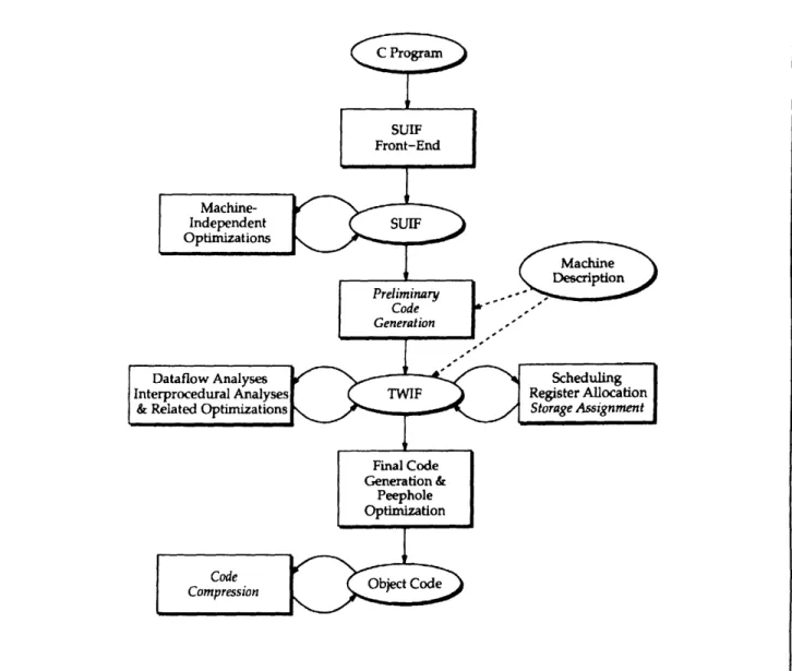
In our experimental framework, we use the SUIF Compiler as the front-end to translate source pro-grams from C into the Stanford University Interme-diate Form. (SUIF is the name of the compiler as well as the abbreviation for the intermediate form.) This project currently focuses on several optimiza-tion problems of the back-end. The overall com-piler organization is illustrated in figure 3.A program written in C is first translated into SUIF, which is a largely machine-independent represen-tation of the program. Machine-independent opti-mizations, such as global common subexpression elimination and dead code elimination, are per-formed at this stage. Then, the program is
trans-lated via a preliminary code generation stage into another intermediate form called TWIF. The
prelim-inary code generated is produced from a rule-based machine description written in OLIVE. OLIVE is a language for writing tree-matchers based on dynamic programming. If tree-covering for prelimi-nary code generation is desired, OLIVE allows for compact specifications of code generators.
TWIF serves as a secondary intermediate form that captures some machine-dependent information such as most of the instruction set, while remaining largely machine-independent in form (e.g., call graph representation of the program and control-flow graph representation of the procedures). The purpose of this secondary intermediate form is to support optimizations which are to some extent
Tools
Hardware-Softe
Chapter 1. Custom Integrated Circuits
Figure 3. Overall compiler organization.
machine-dependent, but whose basic formulations and algorithms can be shared across a range of architectures. These optimizations include those based on global data-flow analyses, refinements to the schedule produced by the preliminary code gen-eration phase, traditional register allocation, storage assignment, and interprocedural analyses and opti-mizations.
It is the task of the final code generation phase to translate macros and pseudo-instructions into actual target machine instructions. Also, because interpro-cedural analysis is performed in the TWIF interme-diate form, this phase assumes the task of
resolving symbolic addresses of global variables and procedures as well. Along with this step, we can perform peephole optimizations to eliminate redundancy that may have been neglected in earlier phases or may have arisen from the translation of macros and pseudo-instructions. With peephole optimization the compiler attempts to find small sequences (using a sliding peephole) in the assembly or object code and either remove useless instructions in the sequences or replace the sequences with shorter ones. Finally, if further reduction in code size is desired, code compression can be applied to the object code.
Chapter 1. Custom Integrated Circuits
1.4 VLSI Design for Low-Power
Dissipation
Sponsors
Mitsubishi Corporation National Science Foundation/
Young Investigator Award Fellowship MIP 92-58376
Project Staff
Professor Srinivas Devadas, Professor Anantha P. Chandrakasan, Farzan Fallah, George I.
Hadjiyiannis, Jos6 C. Monteiro
1.4.1 Design for Low Power
Average power dissipation has emerged as an important parameter in the design of general-purpose and application-specific integrated circuits. Optimization for low power can be applied at many different levels of the design hierarchy. For instance, algorithmic and architectural transforma-tions can trade off throughput, circuit area, and power dissipation; and logic optimization methods have been shown to have a significant impact on the power dissipation of combinational logic circuits. It is important to develop optimization methods that are applicable to a broad class of circuits. To this end, we are developing a synthesis system capable of synthesizing low-power digital combinational and sequential circuits from high-level descriptions. Our recent work in this area is described in the section on scheduling. We are also issues involving the design of low-bandwidth protocols for remote termi-nals that can be implemented using low-power cir-cuits. This work is described in the section on protocols.
1.4.2 Shutdown Techniques
It has been demonstrated at the gate and system levels that large power savings are possible merely by cutting down on wasted power--commonly referred to as power management. At the system level, this involves shutting down blocks of hard-ware that are not being used. Detection and shut down of unused hardware is done automatically in current generations of Pentium and PowerPC processors. The Fujitsu SPARClite processor pro-vides software controls for shutting down hardware.
Graduate student Jos6 Monteiro applied power management techniques at the sequential logic and combinational logic levels in 1994. Application of power management at the gate level involves first identifying large portions of the circuit that fre-quently7 produce information that is either not essential for determining the values on the primary outputs, or information that could have been produced by much simpler hardware. Additional hardware is then added to the circuit that detects on a per-clock-cycle basis input conditions under which such a situation arises and shuts down the corresponding portions of the circuit for that clock cycle.
During 1995, Mr. Monteiro introduced power man-agement into scheduling algorithms used in behavioral-level synthesis. Behavioral synthesis comprises of the sequence of steps by means of which an algorithmic specification is translated into hardware. These steps involve breaking down the algorithm into primitive operations and associating each operation with the time interval in which it will be executed (called operation scheduling) and the hardware functional block that will execute it (called hardware allocation). Clock-period constraints, throughput constraints, hardware resource con-straints, and their combination make this a non-trivial optimization problem.
Decisions taken during behavioral synthesis have a far reaching impact on the power dissipation of the resulting hardware. For example, throughput-improvement by exploiting concurrency via transfor-mations like pipelining and loop unrolling enables the hardware to be operated at lower clock fre-quencies and thereby at lower voltages. The lower supply voltage leads to a reduction in power
dissi-pation.
Our work is centered around the observation that scheduling has a significant impact on the potential for power savings via power management. Based on this observation, we have developed a sched-uling algorithm that is power-management-aware,
i.e., it generates a schedule that maximizes the potential for power management in the resulting hardware. The algorithm operates under a user determined combination of throughput, cycle-time
and hardware resource constraints. Starting from a high-level description, our implementation of the algorithm generates a logic implementation for the controller as well as the datapath corresponding to the power-management-aware schedule.
Chapter 1. Custom Integrated Circuits
1.4.3 Protocols
The easiest way of reducing the power consump-tion of any computing device is to reduce the amount of computation it performs. A portable computer (hereafter called the terminal) can do just enough work to manage the input and output devices and defer all other computation to a sepa-rate cycle server (hereafter called the stationary cycle server or just cycle server for short) that will actually perform all the computationally intensive tasks. The terminal and the cycle server can be connected in such a fashion as to allow the terminal to transmit all input to the cycle server and the cycle server to transmit all output back. Then the cycle server can be made stationary, and therefore have an external power source. If the connection method is wireless, then the terminal becomes effectively a portable computer. Since the cycle server has an external power source, only the con-sumption of the terminal needs to be reduced. This becomes an easier task since the terminal can be designed to perform the minimal amount of compu-tation necessary to manage the input and output devices. Nonetheless, to the user, the terminal appears to have all the processing power of the stationary cycle server.
The main problem with the above scheme is the bandwidth requirement between the terminal and the cycle server. Especially for color terminals this bandwidth can very easily become excessive. graduate student George I. Hadjiyiannis has devel-oped a protocol for a wireless remote terminal which emphasizes low bandwidth and low power requirements. Rather than using a hardwired pro-tocol, it was decided that general-purpose processor would be used, highly optimized for the task at hand. Thus, the terminal and its protocol would become infinitely flexible, allowing us to make use of better algorithms, new extensions to the X-server, and to make additions and modifica-tions to the protocol at will. Then a more complex protocol was designed which reduces the band-width requirements while allowing the use of color. This was accomplished by giving the protocol the notion of higher level elements (for example, rec-tangles, polygons, lines, etc.), the protocol requires much less information to perform the same activ-ities. For example, if the protocol had a notion of what a text character is, one would only need to send a command that identifies the character, its position, and the color to which it should be drawn, rather than sending a complex bitmap over the link. Error correction and retransmission methods capable of dealing with burst error noise up to BERs of 10- 3 were developed The average band-width required by the protocol is 140 Kbits/sec for
8-bit color applications including the overhead for error correction.
1.4.4 Publications
Journal ArticlesLin, B., and S. Devadas. "Synthesis of Hazard-Free Multilevel Logic Under Multiple Input Changes from Binary Decision Diagrams." IEEE Trans. Comput.-Aided Des. 14(8): 974-985 (1995).
Monteiro J., S. Devadas, and A. Ghosh. Sequential Circuits for Low Power." High-Speed Logic. Forthcoming.
"Retiming
Inter. J.
Monteiro J. and S. Devadas. "Techniques for Power Estimation and Optimization at the Logic Level: a Survey." J. VLSI Signal Process. Forthcoming.
Monteiro J., S. Devadas, A. Ghosh, K. Keutzer, and J.K. White. "Estimation of Average Switching Activity in Combinational Logic Circuits Using Symbolic Simulation." IEEE Trans. Comput.-Aided Des. Forthcoming.
Shen, A., S. Devadas, and A. Ghosh. "Probabilistic Manipulation of Boolean Functions Using Free Boolean Diagrams." IEEE Trans. Comput.-Aided Des. 14(1): 87-95 (1995).
Tsui, C-Y., J. Monteiro, M. Pedram, S. Devadas,
A.M. Despain, and B. Lin. "Power Estimation Methods for Sequential Logic Circuits." IEEE Trans. VLSI Syst. 3(3): 404-416 (1995).
Conference Proceedings
Devadas, S., and S. Malik. "A Survey of Optimiza-tion Techniques Targeting Low Power VLSI Cir-cuits." Paper published in the Proceedings of the 32nd Design Automation Conference, San Francisco, California, June 1995, pp. 224-247. Liao, S., S. Devadas, K. Keutzer, S. Tjiang, and A.
Wang. "Storage Assignment to Decrease Code Size." Paper published in the Proceedings of the SIGPLAN Programming Language Design and Implementation Symposium, Princeton, New Jersey, June 1995, pp. 186-195.
Liao, S., S. Devadas, K. Keutzer, S. Tjiang, and A. Wang. "Code Optimization Techniques in Embedded DSP Microprocessors." Paper pub-lished in the Proceedings of the 32nd Design
Chapter 1. Custom Integrated Circuits
Automation Conference, San Francisco, California, June 1995, pp. 599-604.
Liao, S., S. Devadas, K. Keutzer, and S. Tjiang.
"Instruction Selection Using Binate Covering for Code Size Optimization." Paper published in the Proceedings of the International Conference on Computer-Aided Design, San Jose, California, November 1995, pp. 393-399.
Liao, S., S. Devadas, and K. Keutzer. "Code Density Optimization for Embedded DSP Processors Using Data Compression Tech-niques." Paper published in the Proceedings of the 1995 Chapel Hill Conference on Advanced Research in VLSI, Chapel Hill, North Carolina, March 1995, pp. 272-285.
Monteiro J., J. Rinderknecht, S. Devadas, and A. Ghosh. "Optimization of Combinational and Sequential Logic Circuits for Low Power Using Precomputation." Paper published in the Pro-ceedings of the 1995 Chapel Hill Conference on Advanced Research in VLSI, Chapel Hill, North Carolina, March 1995, pp. 430-444.
Monteiro, J., and S. Devadas. "Techniques for the Power Estimation Sequential Logic Circuits Under User-Specified Input Sequences and Pro-grams." Paper published in the Proceedings of the International Symposium on Low Power Design, Dana Point, California, April 1995, pp.
33-38.
1.5 Parallel Algorithms for Device
Simulation
Sponsors
Defense Advanced Research Projects Agency/
U.S. Navy - Office of Naval Research
Contract N00014-94-1-0985 IBM Corporation
National Science Foundation Grant MIP 91-17724
Project Staff
Dr. Andrew Lumsdaine, Mark W. Reichelt, Pro-fessor Jacob K. White, Professor Jonathan Allen The growing importance of mixed circuit/device
sim-ulation, its enormous computational expense, as well as the increasing availability of parallel com-puters, have made the development of specialized, easily parallelized, algorithms for transient
simu-lation of MOS devices necessary. In earlier work on the waveform overrelaxation device simulator (WORDS) program, the easily parallelized wave-form relaxation (WR) algorithm was shown to be a computationally efficient approach to device tran-sient simulation even on a serial machine. However, the WR algorithm typically requires hun-dreds of iterations to achieve an accurate solution. To use WORDS in a mixed circuit/device simulator, we have been investigating ways of making WORDS more robust and efficient. We determined how to compute the terminal currents accurately using different timepoints at different mesh nodes. We also improved the timestep selection procedure by determining how to refine the timesteps as WR iterations proceed. Then we reduced the total com-putation by as much as a factor of 2 by using only a few coarse timesteps in early iterations. The more accurate electric field dependent mobility model was also implemented. Recent work on the-oretical aspects of these methods have answered several long-standing questions about multirate sta-bility.8
We found experimental evidence that WR using standard overrelaxation acceleration can produce oscillatory results and are investigating methods for eliminating this phenomenon. A frequency-dependent overrelaxation algorithm using lowpass filtering was developed, as well as a waveform
8 A. Lumsdaine, M. Reichelt, and J. White, "Accelerated Waveform Methods for Parallel Transient Simulation of Semiconductor Devices," IEEE Trans. Comput.-Aided Des., forthcoming.
Chapter 1. Custom Integrated Circuits
conjugate-direction approach.9 Experimental results indicate that both approaches reduce the number of waveform iterations required by more than a factor of seven. Finally, experimental results show that although the accelerated WR methods are as fast as the best of the standard algorithms for device transient simulation on a serial machine, WR algo-rithms are substantially faster on a parallel machine.9
1.6 Numerical Simulation of Short
Channel MOS Devices
Sponsors
IBM Corporation
U.S. Navy - Office of Navel Research Contract N00174-93-K-0035
Project Staff
Khalid Rahmat, Professor Dimitri A. Professor Jacob K. White
Antoniadis,
The model used in conventional device simulation
programs is based on the drift-diffusion model of electron transport, and this model does not accu-rately predict the field distribution near the drain in small geometry devices. This is of particular impor-tance for predicting oxide breakdown due to pene-tration by "hot" electrons. There are two approaches for more accurately computing the elec-tric fields in MOS devices: one is based on adding an energy equation to the drift-diffusion model, and the second is based on direct solution of Boltzman's equation.
Energy-balance based simulation programs are limited in their ability to accurately predict hot-electron effects, and we have been investigating efficient techniques for solving the full Boltzman equation using a spherical-harmonics-based approach. We have implemented a Galerkin method for the solution of the Boltzmann equation which allows arbitrary order spherical harmonic expansions in momentum space. A self-consistent
solution is obtained by directly solving the Boltzmann and Poisson equations simultaneously. The boundary conditions and discretization methods necessary for the arbitrary order method have also been investigated. Results up to third order in one real space dimension show the importance of including harmonics beyond first order to accurately calculate the distribution function in high field
regions.10
1.7 Coupled Simulation Algorithms for
Microelectromechanical CAD (MEMCAD)
Sponsors
Analog Devices Corporation
Federal Bureau of investigation
Contract J-FBI-92-196
Project Staff
Narayana R. Aluru, Mattan Kamon, Professor Martin A. Schmidt, Professor Stephen D. Senturia, Professor Jacob K. White
High fabrication costs and increasing microsensor complexity is making computer simulation of the
realistic geometries necessary, both to investigate design alternatives and to perform verification before fabrication. At MIT, we are developing a
microelectromechanical computer-aided design
(MEMCAD) system to make it possible for
micro-sensor designers to easily perform realistic simu-lations. Carefully selected commercial software packages have been linked with specialized data-base and numerical programs to allow a designer to easily enter a three-dimensional microsensor geom-etry and quickly perform both mechanical and elec-trical analysis. The system currently performs electromechanical analyses, such as calculating the capacitance versus pressure (or force) curve for
both a square diaphragm deformed by a differential pressure, and can be used to calculate levitation
forces in structures as complicated as a comb
drive."
9 A. Lumsdaine and J. White, "Accelerating Waveform Relaxation Methods with Application to Parallel Semiconductor Device
Simu-lation," Numerical Functional Analysis and Optimization, forthcoming; M. Reichelt, J. White, and J. Allen, "Optimal Convolution SOR Acceleration of Waveform Relaxation with Application to Parallel Simulation of Semiconductor Devices," SIAM J. Sci. Stat. Comput., forthcoming.
10 K. Rahmat, J. White, and D. Antoniadis, "A Galerkin Method for the Arbitrary Order Expansion in Momentum Space of the Boltzmann
Equation using Spherical Harmonics," Proceedings of NUPAD V, Honolulu, Hawaii, June 1994; K. Rahmat, J. White, and D.A. Antoniadis, "Solution of the Boltzmann Transport Equation in Two Real-Space Dimensions using a Spherical Harmonic Expansion in Momentum Space," Proceedings of the International Electron Devices Meeting, San Francisco, California, December 1994.
11 X. Cai, P. Osterberg, H. Yie, J. Gilbert, S. Senturia, and J. White, "Self-Consistent Electromechanical Analysis of Complex 3-D
Chapter 1. Custom Integrated Circuits
To support design of electromechanical structures, we are currently investigating two approaches to combining finite-element mechanical analysis with multipole-accelerated electrostatic analysis. The first method is the obvious relaxation algorithm and the second method is a more sophisticated sur-face/Newton generalized conjugate-residual scheme. By comparing the two methods, we have demonstrated both theoretically and by example that our surface/Newton-GCR algorithm is faster and more robust than the simplier relaxation scheme.'2 We have also been working on the multi-pole accelerated Galerkin implementation of our electrostatic analysis program FASTCAP. The motivation for this is that Galerkin is less sensitive to the mesh of the structure than the original collo-cation approach and, particularly with dielectric interfaces, yields more accurate results.'3
We have also been investigating how to apply CAD to MEMS with the level of complexity of a practical, high-yvolume manufacturable sensor while avoiding computationally impractical models. Two methods were developed. One was a simple analysis method in which the ideal structure was assumed.
This allowed prediction of the stability and the effects of structure misalignment on a surface-micromachined accelerometer. However, the simple method is limited because the actual struc-ture has fabrication induced non-idealities, such as warpage, which can cause the simple method to be significantly in error. The second method discarded the ideal structure assumption and analyzed the non-ideal structure via a self-consistent analysis. This method is based on the calculation of an inter-mediate look-up table from which the electrostatic forces are obtained directly from the position of the moving mass, greatly reducing computation time and memory requirements in comparison to a stan-dard self-consistent electromechanical analysis scheme. Using this lumped-model self-consistent scheme, we analyzed an Analog Devices, Inc.
ADXL50 accelerometer including fabrication
non-idealities (warpage, over-etching, residual stress, etc). 4
Finally, in our latest work we investigate the cou-pling of fluid forces and mechanical deformation to add additional capabilities to our existing MEMCAD system. To gain more control over the underlying algorithms of the current MEMCAD system first, we are currently implementing an elastostaic solver to replace the commerical mechanical solver used in the MEMCAD system.
1.8 Numerical Techniques for
Simulating Josephson Junction Arrays
Sponsors
Defense Advanced Research Projects Agency/ Consortium for Superconducting Electronics
Contract MDA 972-90-C-0021
National Defense Science and Engineering Graduate Fellowship
Project Staff
Joel R. Phillips, Dr. Herre S.J. van der Zant, Pro-fessor Terry Orlando, ProPro-fessor Jacob K. White Vortices play a central role in determining the static and dynamic properties of two-dimensional (2-D) superconductors. Artificially fabricated networks of superconducting islands weakly coupled by Josephson junctions are model systems to study the behavior of vortices. Through simulation, we have discovered that the static properties of vortices in an array of Josephson junctions can be significantly influenced by magnetic fields induced by the vortex currents. The energy barrier for vortex motion is enhanced, nearly doubling for penetration depths on the order of a cell size. Moreover, we have found that correct calculation of the vortex current distribution, the magnetic moment, and the lower critical field require modeling mutual induc-tance interactions between all cell pairs in the array. To make numerical simulation of the system with all inductive effects computationally feasible, a novel
FFT-accelerated integral equation solver was derived. This algorithm is sufficiently efficient to
12 H. Yie, X. Cai, P. Osterberg, S. Senturia, and J. White, "Convergence Properties of Relaxation versus the Surface-Newton Generalized-Conjugate Residual Algorithm for Self-consistent Electromechanical Analysis of 3-D Micro-Electro-Mechanical Struc-tures," Proceedings of NUPAD V, Honolulu, Hawaii, June 1994.
13 X. Cai, K. Nabors, and J. White, "Efficient Galerkin Techniques for Multipole-Accelerated Capacitance Extraction of 3-D Structures
with Multiple Dielectrics," Proceeding of the 16th Conference on Advanced Research in VLSI, Chapel Hill, North Carolina, March 1995.
14 H. Yie, S.F. Bart, J. White, and S.D. Senturia, "Computationally Practical Simulation of a Surface-Micromachined Accelerometer with True Fabrication Non-idealities," Proceedings of MEMS 95,.