HAL Id: hal-02267953
https://hal.archives-ouvertes.fr/hal-02267953
Submitted on 25 Aug 2020HAL is a multi-disciplinary open access archive for the deposit and dissemination of sci-entific research documents, whether they are pub-lished or not. The documents may come from teaching and research institutions in France or abroad, or from public or private research centers.
L’archive ouverte pluridisciplinaire HAL, est destinée au dépôt et à la diffusion de documents scientifiques de niveau recherche, publiés ou non, émanant des établissements d’enseignement et de recherche français ou étrangers, des laboratoires publics ou privés.
Optoelectronic properties of methyl-terminated
germanane
Clément Livache, Bradley Ryan, Utkarsh Ramesh, Violette Steinmetz, Charlie
Gréboval, Audrey Chu, Thibault Brulé, Sandrine Ithurria, Geoffroy Prévot,
Thierry Barisien, et al.
To cite this version:
Clément Livache, Bradley Ryan, Utkarsh Ramesh, Violette Steinmetz, Charlie Gréboval, et al.. Op-toelectronic properties of methyl-terminated germanane. Applied Physics Letters, American Institute of Physics, 2019, 115 (5), pp.052106. �10.1063/1.5111011�. �hal-02267953�
1
Optoelectronic Properties of Methyl-Terminated Germanane
Clément Livache
1,2, Bradley J. Ryan
3, Utkarsh Ramesh
3, Violette Steinmetz
1, Charlie Gréboval
1, Audrey Chu
1,
Thibault Brule
4, Sandrine Ithurria
2, Geoffroy Prevot
1, Thierry Barisien
1, Abdelkarim Ouerghi
5, Matthew G.
Panthani
3, Emmanuel Lhuillier
1*1
Sorbonne Université, CNRS, Institut des NanoSciences de Paris, 4 place Jussieu, 75005 Paris, France
2Laboratoire de Physique et d’Etude des Matériaux, ESPCI-Paris, PSL Research University, Sorbonne
Université Univ Paris 06, CNRS UMR 8213, 10 rue Vauquelin, 75005 Paris, France.
3
Department of Chemical and Biological Engineering, Iowa State University, Ames, IA 50011, USA
4HORIBA Scientific, HORIBA France S.A.S, Avenue de la Vauve, Passage Jobin Yvon, 91120 Palaiseau, France
5
Centre de Nanosciences et de Nanotechnologies, CNRS, Univ. Paris-Sud, Université Paris-Saclay, C2N –
Marcoussis, 91460 Marcoussis, France
Abstract : Germanane is a two-dimensional (2D), strongly confined form of germanium. It presents an interesting combination of (i) ease of integration with CMOS technology, (ii) low toxicity, and (iii) electronic confinement which transforms the indirect band gap of the bulk material into a direct bandgap featuring photoluminescence. However, the optoelectronic properties of this material remain far less investigated than its structural properties. Here, we investigate the photoluminescence and transport properties of arrays of methyl-terminated germanane flakes. The photoluminescence appears to have two contributions, one from the band edge and one from trap states. The dynamics of the exciton appear to be in the 1-100 ns range. Conduction in this material appears to be p-type, while the photoconduction time response can be made as short as 100 µs.
Keywords : germanium monolayer, germanane, field effect transistor, luminescence, electronic transport. * To whom correspondence should be sent: el@insp.upmc.fr
2 Nanocrystals have raised substantial interest over the past years owing to their broadly tunable band edge energy, ranging from the ultraviolet to terahertz spectral regions.1,2 Nanocrystals are now commonly used as green
light-emitters for display technologies3 or as chlorophyll-optimized down-converters for agricultural lighting. In all of these
applications, nanocrystals are optically pumped. More advanced applications such as LED or photodetectors4 will
require films of nanocrystals with suitable transport properties.
Currently, most nanocrystals are based on II-VI and III-V compound semiconductors that possess optical properties in the visible range, but contain toxic elements and are difficult to integrate with CMOS technology.5 In this sense,
nanocrystals made from Group IV compounds are of utmost interest. However, Si6,7 and Ge8,9 nanocrystals have been
far less investigated than other materials such as CdSe and PbS, in particular due to their sensibility to oxidation. Beyond these 0D quantum dots, 2D forms a Ge and Si, analogous to graphene, have also generate a strong interest over the recent years. Atomically-thin sheets of Si or Ge (known as silicene10 and germanene11, respectively) have been
proposed as alternative to graphene; however, their feasibility and stability of remain controversial.12 In addition, the
band gap of silicene and germanene is expected to be very narrow,13 which make them poor candidates for
optoelectronic applications in spite of their low effective masses induced by the Dirac cones. In addition and contrary to graphene, silicene and germanium cannot be separated from their substrate, this makes their device integration even more challenging. It is nevertheless possible to grow 2D sheets of Si and Ge terminated by either hydrogen or methyl groups.14–18 This form of weakly-coupled Si and Ge 2D-flakes are called silicane and germanane,19–21 and they
present a strong confinement leading to a band gap (1.8 eV for germanane) compatible with electronic and optical applications in the visible region. In addition, their effective masses are expected to be small, which could lead to high carrier mobilities.22 While the electronic structure23 and structural properties22,24 of these materials have been widely
investigated, especially by the Goldberger group,14 device integration remains limited.25–27 Here, we investigate the
optoelectronic properties of methyl-terminated germanane. We unveil their transport and spectroscopic properties which will be of utmost interest for future design of devices based on germanane.
3
Figure 1 Dark-field optical (a.), scanning electron (b.) and transmission electron (c.) microscopy images of the methy-terminated germanane flakes. FTIR (d.) and Raman (e.) spectra of methyl-methy-terminated germanane powder. (d.) Powder X-ray diffraction pattern of methyl-terminated germanane; the narrow peak highlighted with a ‘*’ corresponds to bulk Ge.
We synthesized methyl-terminated germanane flakes by modifying a procedure reported by Jiang et. al,14 see
Supplementary Informations for details. The obtained flakes have large lateral dimensions reaching several microns, as revealed by microscopy images in Figure 1a-c. These germanane flakes are comprised of stacks of individual layers (20-50 nm in thickness typically) of methyl-terminated germanane, as revealed by the TEM image, see Figure 1c. The Fourier-transform infrared (FTIR) spectroscopy confirms the presence of methyl termination, with vibrational modes arising from C-H and Ge-C bonds, see Figure 1d. The Raman spectrum (see Figure 1e) reveals a main contribution appearing at 299 cm-1 which is associated with the E
2g mode.21,28 A second contribution arising from the methyl
functionalization appears at 594 cm-1. The X-ray diffraction15,18,29 (Figure 1f) in particular reveals a peak around 2θ ≈
7.9°, which along with Raman and Fourier transform infrared spectroscopy, confirms that the sample contains Ge sheets that are terminated with -CH3 groups.15 From Bragg’s law the periodicity of the material is found to be ≈ 1.1
nm, corresponding to an interplanar distance of 0.55 nm.
A key interest for this confined form of germanane is the presence of luminescence in the visible range; this is in contrast with the bulk material which presents no luminescence due to the indirect nature of its band gap. As such, methyl-terminated germanane is a very promising candidate for the fabrication of light-emitting diodes (LEDs). Indeed, current organic and nanocrystal-based LEDs suffer from low light extraction, which limits their conversion efficiency to 20%. This limitation is the result of isotropic emission of photons, which makes that most emitted light is lost due to total internal reflections. Here, due to its 2D geometry, germanane is expected to have anisotropic emission which
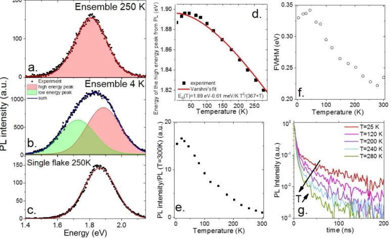
4 may improve light extraction.30 The photoluminescence (PL) peak of germanane appears around 700 nm (1.8 eV)
around room temperature, see Figure 2a.
The full width at half maximum (FWHM) of the PL is ≈ 200 meV. Analysis of the temperature dependence of the PL reveals that, with decreasing temperature, the PL intensity increases (Figure 2e and S1) and broadens (Figure 2f and S2). At high temperatures (>200 K), the ensemble PL signal is well fitted by a single Gaussian distribution (see Figure S1b); the energy of the transition appears at 1.8 eV, which correspond to the predicted transition for the 2H phase of germanane.19 PL measurements on a single flake at (250 K) reveals a PL signal with a similar linewidth, see Figure 2c.
This suggests that the PL linewidth is the result of a homogeneous broadening. At low temperatures, a second contribution appears in the PL signal, see Figure 2b, and is responsible for the observed broadening of the PL signal. Since the signal appears at an energy lower than the band gap value, it is attributed to trap states. Note that depending on the relative weight of the two contributions the PL peak may sometimes appears at lower energy in the literature.15
Fitting the high energy contribution (i.e. at the band edge) of the PL with a Varshni’s expression 𝐸𝐺(𝑇) = 𝐸𝐺(𝑇 = 0𝐾) −
𝐴.𝑇2
𝑇+𝜃 allows for the determination of the temperature dependence of the band gap with A = 610 µeV/K and the phonon temperature 𝜃 = 367 K. For the sake of comparison, the value of phonon temperature31
has been found to be 374 K in the bulk, while the temperature dependence of the band gap is slightly lower at 460 µeV/K.
Figure 2 Photoluminescence (PL) spectra of methyl-terminanted germanane flakes: ensemble measurement at 250 K (a.), ensemble measurement at 4 K (b.), and (c.) single flake measurement at 250 K (In all case experimental data are points and full curve are Gaussian (or two Gaussian sum) fit.) (d.) Temperature dependence of the energy of the low energy peak and its Varshni‘s fit. (e.) PL intensity as a function of temperature for a film of methyl-terminated germanane flakes. (f.) Full width at half maxium (FWHM) of the PL signal as a function of temperature for a film of terminanted germanane flakes. (g.) Time resolved PL, integrated over the whole spectrum, for a film of methyl-terminanted germanane flakes at various temperature. The arrow shows the trend for the carrier decay as temperature is increased.
5 Time-resolved PL, (Figure 2g and S3), reveals multi exponential behavior. At room temperature, three characteristic lifetimes can be extracted: 2 ns, 20 ns and 100 ns. After 2 µs, the PL signal has fully decayed. We observe that the lifetime increases as temperature decreases. This is correlated with increased trap emission at low temperatures, suggesting that the rate of trap-assisted recombination is slower than band-to-band recombination. To further confirm this hypothesis, we have check that the dynamic relative to the low energy part of the PL peak is slower than the one relative to the high energy part of the PL peak, see Figure S3b.
To assess the electronic transport properties of germanane flake arrays, we constructed interdigitated electrodes using conventional optical lithography method and drop-casted a dispersion of germanane flakes was onto the electrodes. Figure 3b shows I-V characteristics of the germanane flake array at different temperatures. The arrays appears to be conductive, with decreasing conductance with decreasing temperature. Fitting the current-temperature curve to an Arrhenius law (Figure 3c) allows for the extraction of an activation energy of 118 meV in the vicinity of room temperature. Because this activation energy is much smaller than one half of the band gap — the expected value for intrinsic semiconductors — this suggests residual doping within the material. To determine the nature of this doping, we integrated the material in a field effect transistor. We use an ion gel electrolyte gating which has proven to be a viable approach for field effect transistor with low gate bias using colloidal nanocrystals32 and 2D materials33
as the channel material as shown in the schematic in Figure 3a. This strategy has been particularly successful for achieving gating in thick, heterogeneous films while allowing stable operating in ambient air.34 The transfer curve
(Figure 3d) reveals p-type character (i.e. a rise of conductance under hole injection at negative gate biases) for the methyl-terminated germanane flake arrays; this is consistent with previous observations obtained using a back gated geometry.26 The on/off ratio of the transistor reached a factor 250 over only ±2 V of gate bias operation. It is also
worth pointing that the turn-on voltage of the transistor is around 100 mV, which is very similar to the activation energy determined from the I-T curve. This suggests that the Fermi level of the material lies in the vicinity (100±20 meV) of the valence band.
6
Figure 3 (a.) Diagram of an electrolyte gated field effect transistor, in which the channel is made of a dense film of methyl-terminated germanane flakes. (b.) IV curve for a thin film of methyl-terminated germanane flakes at various temperatures. (c.) Current as a function of temperature for a thin film of methyl-terminated germanane flakes at various temperatures under +5 V bias. d. Transfer curve (drain and gate current as a function of the applied gate bias) for an electrolyte gated field effect transistor in which the channel is made of a dense film of methyl-terminated germanane flakes at room temperature. The drain source bias is set at -100 mV.
Under illumination, arrays of methyl-terminated germanane flakes display positive photoresponse (i.e. a rise in conductance under illumination), as shown in Figure 4a. The time response of the device is typically below 100 µs with a weak temperature dependence. This corresponds in the frequency domain to a 3 dB cut-off frequency above 1 kHz, see Figure 4b. The power dependence of the photoresponse appears to present a power law dependency where the exponent is close to 0.5, as shown in Figure 4c. This suggests that the photocarrier lifetimes are limited by a bi-molecular process35,36 (i.e. band-to-band recombination), rather than by trapping. This observation is consistent the
absence of traps in the PL spectrum at room temperature.
Figure 4 (a.) Current as a function of time while the sample is illuminated by a pulse of light (λ = 405 nm, P ≈ 2 mW), at different temperatures. The measurement is made under a +5 V bias. (b.) Frequency dependence of the photocurrent, at room temperature. (c.) Current as a function of light incident power. Measurements are obtained at room temperature under 5 V bias.
In conclusion, we have investigated the photoluminescence and electronic transport properties of methyl-terminated germanane flakes. The PL signal of the flakes was found to have two contributions: one from the band edge, and another that is attributed to trap states. The PL linewidth is found to have an homogeneous origin and a carrier lifetimes in the 1-100 ns range. Arrays of methyl-terminated flakes exhibit p-type conduction. The material is also photoconductive with a fast time response of the order of 100 µs, mostly limited by interband recombination.
ACKNOWLEDEGMENTS
EL acknowledges the financial support of the European Research Council (ERC) starting grant (blackQD – n°756225). We thank Agence Nationale de la Recherche for funding through grant Nanodose and IPER-nano2. This work was supported by French state funds managed by the ANR within the Investissements d'Avenir programme under reference ANR-11-IDEX-0004-02, and more specifically within the framework of the Cluster of Excellence MATISSE. We acknowledge the use of clean-room facilities from the “Centrale de Proximité Paris-Centre”. This work has been supported by the Region Ile-de-France in the framework of DIM Nano-K. This work was partially supported by the Air
7 Force Office of Scientific Research Young Investigator Program (Grant # FA9550-17-1-0170) and the National Science Foundation Early Career Development (CAREER) Award (Award # 1847370). MGP also acknowledges support from the Herbert L. Stiles Faculty Fellowship. BJR acknowledges support from the National Science Foundation Graduate Research Fellowship under DGE 1744592.
"Supplementary Material" include information about material synthesis, material characterization, and additional transport measurements.
Competing financial interests: The authors declare no competing financial interests.
REFERENCES
1 H. Chen, H. Liu, Z. Zhang, K. Hu, and X. Fang, Advanced Materials 28, 403 (2016).
2 N. Goubet, A. Jagtap, C. Livache, B. Martinez, H. Portalès, X.Z. Xu, R.P.S.M. Lobo, B. Dubertret, and E. Lhuillier, J.
Am. Chem. Soc. 140, 5033 (2018).
3 T. Erdem and H.V. Demir, Color Science and Photometry for Lighting with LEDs and Semiconductor Nanocrystals
(Springer Singapore, 2019).
4 B. Martinez, J. Ramade, C. Livache, N. Goubet, A. Chu, C. Greboval, J. Qu, W. Watkins, L. Becerra, E. Dandeu, J.L.
Fave, C. Méthivier, E. Lacaze, and E. Lhuillier, Submitted (2019).
5 E. Georgitzikis, P.E. Malinowski, L.M. Hagclsieb, V. Pejovic, G. Uytterhoeven, S. Guerrieri, A. Süss, C. Cavaco, K.
Chatzinis, J. Maes, Z. Hens, P. Heremans, and D. Cheyns, in 2018 IEEE SENSORS (2018), pp. 1–4.
6 B.T. Diroll, K.S. Schramke, P. Guo, U.R. Kortshagen, and R.D. Schaller, Nano Lett. 17, 6409 (2017). 7 L. Mangolini, E. Thimsen, and U. Kortshagen, Nano Lett. 5, 655 (2005).
8 X. Lu, B.A. Korgel, and K.P. Johnston, Chem. Mater. 17, 6479 (2005).
9 X. Lu, K.J. Ziegler, A. Ghezelbash, K.P. Johnston, and B.A. Korgel, Nano Lett. 4, 969 (2004).
10 P. Vogt, P. De Padova, C. Quaresima, J. Avila, E. Frantzeskakis, M.C. Asensio, A. Resta, B. Ealet, and G. Le Lay, Phys.
Rev. Lett. 108, 155501 (2012).
11 M.E. Dávila, L. Xian, S. Cahangirov, A. Rubio, and G.L. Lay, New J. Phys. 16, 095002 (2014).
12 W. Peng, T. Xu, P. Diener, L. Biadala, M. Berthe, X. Pi, Y. Borensztein, A. Curcella, R. Bernard, G. Prévot, and B.
Grandidier, ACS Nano 12, 4754 (2018).
13 Z. Ni, Q. Liu, K. Tang, J. Zheng, J. Zhou, R. Qin, Z. Gao, D. Yu, and J. Lu, Nano Lett. 12, 113 (2012). 14 S. Jiang, M.Q. Arguilla, N.D. Cultrara, and J.E. Goldberger, Chem. Mater. 28, 4735 (2016).
15 S. Jiang, S. Butler, E. Bianco, O.D. Restrepo, W. Windl, and J.E. Goldberger, Nature Communications 5, 3389 (2014). 16 T.J. Asel, E. Yanchenko, X. Yang, S. Jiang, K. Krymowski, Y. Wang, A. Trout, D.W. McComb, W. Windl, J.E.
Goldberger, and L.J. Brillson, Appl. Phys. Lett. 113, 061110 (2018).
17 Y. Ma, Y. Dai, W. Wei, B. Huang, and M.-H. Whangbo, Scientific Reports 4, 7297 (2014). 18 Z. Liu, Z. Wang, Q. Sun, Y. Dai, and B. Huang, Applied Surface Science 467–468, 881 (2019).
19 G. Coloyan, N.D. Cultrara, A. Katre, J. Carrete, M. Heine, E. Ou, J. Kim, S. Jiang, L. Lindsay, N. Mingo, D. Broido, J.P.
Heremans, J. Goldberger, and L. Shi, Appl. Phys. Lett. 109, 131907 (2016).
20 N.D. Cultrara, Y. Wang, M.Q. Arguilla, M.R. Scudder, S. Jiang, W. Windl, S. Bobev, and J.E. Goldberger, Chem.
Mater. 30, 1335 (2018).
21 E. Bianco, S. Butler, S. Jiang, O.D. Restrepo, W. Windl, and J.E. Goldberger, ACS Nano 7, 4414 (2013). 22 R.K. Ghosh, M. Brahma, and S. Mahapatra, IEEE Transactions on Electron Devices 61, 2309 (2014). 23 H. Shu, Y. Li, S. Wang, and J. Wang, J. Phys. Chem. C 119, 15526 (2015).
24 N.D. Cultrara, M.Q. Arguilla, S. Jiang, C. Sun, M.R. Scudder, R.D. Ross, and J.E. Goldberger, Beilstein Journal of
Nanotechnology 8, 1642 (2017).
25 W. Amamou, P.M. Odenthal, E.J. Bushong, D.J. O’Hara, Y.K. Luo, J. van Baren, I. Pinchuk, Y. Wu, A.S. Ahmed, J.
Katoch, M.W. Bockrath, H.W.K. Tom, J.E. Goldberger, and R.K. Kawakami, 2D Mater. 2, 035012 (2015).
26 B.N. Madhushankar, A. Kaverzin, T. Giousis, G. Potsi, D. Gournis, P. Rudolf, G.R. Blake, C.H. van der Wal, and B.J.
8
27 N.G. Sahoo, R.J. Esteves, V.D. Punetha, D. Pestov, I.U. Arachchige, and J.T. McLeskey, Appl. Phys. Lett. 109, 023507
(2016).
28 M.Q. Arguilla, N.D. Cultrara, M.R. Scudder, S. Jiang, R.D. Ross, and J.E. Goldberger, J. Mater. Chem. C 5, 11259
(2017).
29 A.C. Serino, J.S. Ko, M.T. Yeung, J.J. Schwartz, C.B. Kang, S.H. Tolbert, R.B. Kaner, B.S. Dunn, and P.S. Weiss, ACS
Nano 11, 7995 (2017).
30 W.D. Kim, D. Kim, D.-E. Yoon, H. Lee, J. Lim, W.K. Bae, and D.C. Lee, Chem. Mater. (2019). 31 N.M. Ravindra and V.K. Srivastava, Journal of Physics and Chemistry of Solids 40, 791 (1979).
32 E. Izquierdo, A. Robin, S. Keuleyan, N. Lequeux, E. Lhuillier, and S. Ithurria, J. Am. Chem. Soc. 138, 10496 (2016). 33 H. Henck, D. Pierucci, J. Chaste, C.H. Naylor, J. Avila, A. Balan, M.G. Silly, M.C. Asensio, F. Sirotti, A.T.C. Johnson, E.
Lhuillier, and A. Ouerghi, Appl. Phys. Lett. 109, 113103 (2016).
34 E. Lhuillier, S. Ithurria, A. Descamps-Mandine, T. Douillard, R. Castaing, X.Z. Xu, P.-L. Taberna, P. Simon, H. Aubin,
and B. Dubertret, J. Phys. Chem. C 119, 21795 (2015).
35 L.J. Willis, J.A. Fairfield, T. Dadosh, M.D. Fischbein, and M. Drndic, Nano Lett. 9, 4191 (2009).