HAL Id: in2p3-01082061
http://hal.in2p3.fr/in2p3-01082061
Submitted on 13 Jan 2015
HAL is a multi-disciplinary open access
archive for the deposit and dissemination of
sci-entific research documents, whether they are
pub-lished or not. The documents may come from
teaching and research institutions in France or
abroad, or from public or private research centers.
L’archive ouverte pluridisciplinaire HAL, est
destinée au dépôt et à la diffusion de documents
scientifiques de niveau recherche, publiés ou non,
émanant des établissements d’enseignement et de
recherche français ou étrangers, des laboratoires
publics ou privés.
The SAMPIC Waveform and Time to Digital Converter
E. Delagnes, D. Breton, H. Grabas, J. Maalmi, P. Rusquart, M. Saimpert
To cite this version:
E. Delagnes, D. Breton, H. Grabas, J. Maalmi, P. Rusquart, et al.. The SAMPIC Waveform and
Time to Digital Converter . 2014 IEEE Nuclear Science Symposium and Medical Imaging Conference
(2014 NSS/MIC), and 21st Symposium on Room-Temperature Semiconductor X-Ray and
Gamma-Ray Detectors, Nov 2014, Seattle, United States. �in2p3-01082061�
E. Delagnes
1*, D. Breton
2, H. Grabas
1,3, J. Maalmi
2, P. Rusquart
2, M. Saimpert
1.
Abstract– SAMPIC is a Waveform and Time to Digital
Converter (WTDC) multichannel chip. Each of its 16 channels associates a DLL-based TDC providing a raw time with an ultra-fast analog memory allowing fine timing extraction as well as other parameters of the pulse. Each channel also integrates a discriminator that can trigger itself independently or participate to a more complex trigger. After triggering, analog data is digitized by an on-chip ADC and only that corresponding to a region of interest is sent serially to the DAQ. The association of the raw and fine timings permits achieving timing resolutions of a few ps rms. The paper describes the detailed SAMPIC0 architecture and reports its main measured performances.
Index Terms— Analog-digital conversion, Time measurement, Delay lock loop, Mixed analog-digital integrated circuits, Front-end electronics, CMOS.
I. INTRODUCTION
Time stamping with picosecond accuracy is an emerging technique opening new fields for particle physics instrumentation. For example, it permits the localization of vertices with a few mm precision, thus helping associating particles coming from a common primary interaction even in a high background, or it can be used for particle identification using Time of Flight techniques. It has recently been demonstrated that ps timing accuracy can be reached by sampling the detector signal with ultra-fast digitizers and extracting time information by interpolation of the samples located in the leading edge of the signal [1]-[3]. Moreover, the knowledge of the signal waveform permits extracting other useful parameters like charge, pulse width or rise-time and optimizing the timing extraction algorithm during or even after data taking.
II. INTRODUCING THE NOTION OF WAVEFORM TDC
Standard fast waveform digitizers as well as oscilloscopes are usually based on standard ADCs, often interleaved in order to virtually increase their sampling frequency. But high timing
Manuscript received Dec 31, 2014
* corresponding author; [email protected] 1 CEA/IRFU, Centre de Saclay, 91191 Saclay, France.
2 Laboratoire de L’accélérateur Linéaire from CNRS/IN2P3, Centre
scientifique d’Orsay, Bâtiment 200, 91898 Orsay Cedex, France.
3 Now with SCICPP, Santa Cruz (USA)
precision implies high sampling rate above 1GS/s that generates a huge local data rate at the output of the ADC (>> 10 Gbits/s). This makes the associated digital electronics expensive and power consuming so that this kind of solution is not usable for medium or large scale experiments.
Modern ultrafast analog memories using Switched Capacitor Arrays (SCA) nicely solve this problem [2]-[7] especially in terms of power, space and money budgets but their readout deadtime (~ 2 to 100 µs) may be a limitation. Moreover they require extra electronics to be used as timing systems.
In recent systems, TDCs, either embedded in high-end FPGAs or ASICs, are usually used for time measurement. Here, the information is concentrated into a simple digital integer value, thus reducing drastically the dataflow, which is good for large scale measurement. But TDCs do not provide information on waveform, except under the form of Time Over Threshold (TOT) for those able to measure both edges of the signal. Anyhow, in this case, the precision on the amplitude or charge of the signal remains poor.
The most advanced TDCs are based on the association of a coarse time counter running on the main clock and of Delay Line Loops (DLLs) interpolating the latter. The DLLs can be smartly interleaved in order to improve the resolution. Resolution is given by the DLL step but it is usually limited by stability of calibration or environmental effects. Actually, the weak point of the TDC is to have only a digital input, which means that, as shown in Fig. 1, it requires an extra discriminator to transform the analog signal into digital.
This discriminator introduces additional jitter and always suffers from residual time walk – which is the dependency of timing with signal amplitude – even in its most advanced implementation (CFD), or after correction using the TOT information. Thus the overall timing resolution is degraded to the quadratic sum of the discriminator and TDC respective timing resolutions, usually above 25 ps RMS. Moreover, the power consumption of the discriminator necessary to reach good timing performance is usually high.
To overcome all these limitations, we are introducing here the new concept of Waveform TDC, shown in Fig. 1.
The SAMPIC Waveform and Time to Digital
Converter
Fig. 1: the usual implementation of a pure TDC.
An analog memory is added in parallel wi It samples the input signal which can now permits performing an interpolation of the s on the latter. The discriminator is not anymo timing path. Time information is given by as contributions:
- Coarse = Timestamp gray-code Counte - Medium = DLL locked on the clock to interest (100 ps minimum step)
- Fine = samples of the waveform (interp a precision of a few ps RMS)
The time resolution can reach a few ps rm analog signals. Moreover, digitized wavefor and amplitude are available.
III. THE SAMPIC PROJECT
The SAMPIC project is a R&D project ini develop a common WTDC prototype addres high precision timing (5 ps RMS) required and SuperB FTOF. Its natural targets are in fast detectors for Time Of Flight (TOF), parti pile-up rejection (ATLAS AFP…), TOF-PET PMTs, diamonds, APDs, SiPMs, and characterization test benches.
The goals for the first prototype were the follo • Design of a new ASIC called SamPic0
of the Waveform TDC structure. • Evaluation of AMS 0.18µm CMOS
mixed design.
• Design of a system where the mult already usable in a real environmen connected to detector with a real re system.
SamPic0 was designed to be the core of a f free” or more complex chips.
ith the delay line. w be analog and
samples recorded ore in the critical sociation of three er (few ns step) o define region of
polation will give ms, even on small rm shape, charge
itially intended to ssing the need for by ATLAS AFP ndeed all the new cle identification, T, based on
MCP-their associated owing ones:
for the validation S technology for
tichannel chip is nt, which means eadout and DAQ future “dead-time
IV. THE SAMPIC0ASIC
A. Generalities and principle
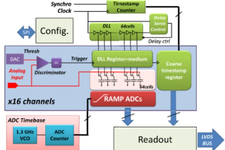
SamPic0 is a 16-channel ASIC. the (externally amplified) analog detector, via an AC-coupling locat elements of the chip architecture listed below:
• 16 single-ended channels, discriminator with pro independent and self-triggere Trigger or External Trigger); • 64 analog switched-capacitor
channel;
• One 11-bit ADC per cell, wh of 64 x 16 = 1024 on-chip AD • One common 12-bit gray-co 160 MHz) for coarse time stam • One common 64-step DLL
clock period of the aforemen running between 1 and 10 G timing & providing the sig sampling;
• One other common 11-bit gra 1.3GHz, used for the mass ADCs;
• One 12-bit LVDS readout b to 400 MHz);
• A SPI Link for internal regist
Fig. 2: Simplified block diagram of SamP
The time tagging sequence for following. When the discriminator o • catches the state of the
timestamp (down to 6.4 ns ste • catches the state of the precision (down to 100 ps step • stops the waveform samplin
ps time precision after interpo samples.
Fig. 3 shows the layout and the i on its board. Its main characteristics
Its inputs directly receive g signal coming from the ted on the board. The main e, depicted in Fig. 2, are
each equipped with a ogrammable threshold, ed (OR with Central OR r-based sampling cells per hich corresponds to a total DCs;
ode counter (running up to mping;
L, servo-controlled to the ntioned gray-code counter, GS/s, for medium precision gnal required for analog ay-code counter running @
sively parallel Wilkinson us (potentially running up ters configuration.
ic0.
r a given channel is the output fires, it:
counter output: coarse eps)
DLL, giving a medium ps)
g which will give the few olation between the analog implementation of the chip
• Technology: AMS CMOS 0.18µm; • Size: 7 mm2;
• Package: 128-pin QFP, pitch of 0.4mm
Fig. 3. Left: layout of SamPic0. Chip is rotated of 90 diagram of Fig. 2. Right: the chip mounted on its board.
B. SAMPIC triggering options
Each channel is equipped with one signal d one 10-bit DAC for each discriminator thres also be external).
As shown in Fig. 4, several trigg programmable individually for each channel “central” trigger (only OR in this chip). Di can be selected. Channels can be disabled. available for post-trigger delay (0, 1, 2 delays A common deadtime optional operation us Enable input is also available.
Fig. 4: triggering options of SamPic0.
When a trigger occurs:
• sampling in the analog memory is sto timestamp is latched;
• the trigger position is recorded in the an • the chip rises a first flag for the user (F ADC conversion and once done with th flag to ask for data readout.
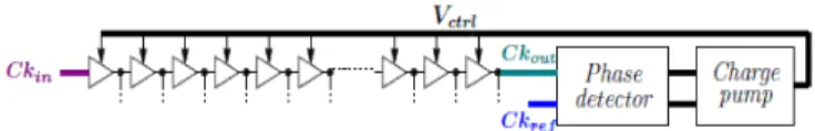
C. DLL and sampling memory
The chip houses a single 64-step long D locked on the Timestamp (TS) counter clock, chip servo-control (phase detector + charge in Fig. 5. It provides 64 incrementally dela constant width used to drive the Track & Hol of the 64 cells for all SCA channels. It prov multiplication’ by 64 of the TS clock (for inst sampling rate will be obtained from a 100 MH T/H signals can be disabled independently (to stop the sampling). An option allowing sampling below 3 GS/s is also available
m.
° clockwise wrt block
discriminator and shold (which can ger modes are l: local, external, iscriminator edge Three option are s of ~1ns). sing a Fast Global
opped and coarse nalog memory; FPGA) to start the
he latter a second
Delay Line Loop , thanks to an on-pump), as shown ayed pulses with ld (T/H) switches vides the ‘virtual tance a 6.4 GSPS Hz TS clock). y on each channel
speed mode for
A special care has been take continuity between last & first cells
Fig. 5: the main DLL of SamPic0.
The chip has no analog input unipolar. The memory cell is based shown in Fig. 6, minimizing the eff pulses (memory persistence). Switch bus during conversion. For these pur • switches 1 and 2 are closed
tracking;
• to sample, switches 1 and 2 then closed to set the poten switches 1 and 2. The cell is th • During few ns before com
switch 2 is closed, then capacitance.
The storage cell capacitance, inc is 35 fF. This values allows a c bandwidth and theoretical kTC noi RMS) for a 11-bit range operation.
The length of 64 cells is a trade-o • Time precision and stability re • Input capacitance requiring a • Time for trigger latency requir
Fig. 6: Left: the 3-switch memory cell of after trigger in order to perform readout a Readout can target a region of interest, wh whole channel.
The chip has been designed to o 1.5 GHz and a usable dynamic rang design has been studied in order (constant bandwidth and constant t the 64 samples (even those located a Analog memory is a circular bu writing until triggering, the oldest ce one turn. As mentioned previous (optionally after a “postrig” delay) and the position of the write point memory. This information is use timing but also as a basis for the o (RoI) mode of readout (only few
en in ensuring a perfect of the DLL.
buffer, and the signal is d on the 3-switch structure
fects of leakages and ghost h 3 also isolates from input rposes:
d while 3 is open during are released. Switch 3 is ntial to the node between
hen in hold mode;
ing back in track mode, n resetting the storage
luding parasitic elements , compact design, 1.5 GHz ise small enough (340 µV
ff for:
equiring a short DLL; short DLL;
ring a long DLL.
f SamPic0. Right: recording stops and analog to digital conversion. hich can be only a subset of the
ffer a signal bandwidth of ge close to 1 V. A special to ensure a good quality tracking duration) over all after trigger).
uffer so it is continuously ells being overwritten after sly, when trigger occurs ), the sampling is stopped ter is tagged in the analog ed for medium precision optional Region of Interest
programmable offset from the trigger) for readout deadtime.
D. Analog to Digital conversion
The schematic principle of the analog to d is shown in Fig. 7.
Fig. 7: schematic principle of the ramp analog to digit
At a given time, all the cells of the channels will be converted simultaneously. The s following:
• Start the on-chip 1.3 GHz Voltage Cont • Enable the 64 ADC comparators of the • Start the on-chip 1.3 GHz gray-code outputs are sent to the channels to conv • Simultaneously start the ramp generato convert: the slope is tunable (speed/pre Conversion time depends on the number o its precision: 1.6 µs for 11bits, 800ns for 8 bi 9 bits … This is actually the main contribu dead time. When the ramp crosses the volta cell, the corresponding counter value is stor Once converted, a channel is immediately usa a new event.
E. Readout philosophy
Readout is driven by Read and RCk signals
Fig. 8: schematic principle of the readout stages.
Data is read channel by channel, with a mechanism to avoid reading always the sa evoked above, an optional RoI readout is av
r minimizing the digital conversion tal conversion. already triggered sequence is the trolled Oscillator enabled channel e counter whose vert ors of channels to cision tradeoff) of bits chosen for
ts, and 400 ns for ution to the input age stored in the red in a register. able for recording
s (see Fig. 8).
a rotating priority ame channel. As vailable to reduce
the dead time (the number of c dynamically). Event data is transm LVDS bus, including:
• Channel Identifier, Timestamp • The value of the converted ce
a given channel, sent sequenti This bus, whose standard spee MWords/s), can potentially run MWords/s). It is worthwhile to noti deadtime during readout, only durin is really a buffer stage).
V. ACQUISITION MODULE AND SOFT
In parallel to the chip design, w electronics module for SamPic0 (see
Fig. 9: SAMPIC acquisition module (left)
The chip is mounted on a mez houses 16 channels, also shown in F mother board which can hold 2 mez a native 32-channel module. Input type. The module is packaged in an (see Fig. 6) and makes use of an switching adaptor power supply. Th and UDP interfaces. Optical links ar active. Power consumption on the channels.
Fig. 10: the SAMPIC acquisition software
We have also developed a grap which permits the full characterizati It is also already usable for small si special visualization for innovative permits visualizing the individual pi exact time location with respe
cells read can be chosen mitted via a 12-bit parallel
ps, Trigger Cell Index; ells (all or a selected set) of
ially.
ed of 1.92 Gbits/s (160 up to 4.8 Gbits/s (400 ice that a channel is not in ng conversion (data register
TWARE
we developed a complete e Fig. 9).
and mezzanine (right).
zzanine board which thus Fig. 9, itself mounted on a zzanines: we thus designed t connectors are of MCX n autonomous metallic box external compact AC/DC he module provides a USB re implemented, but not yet + 5 V is of 1.5 A for 32
e in WTDC display mode.
phical acquisition software ion of the chip and module. ize experiments. It offers a e WTDC mode. The latter ieces of waveforms at their ct to each other. This
functionality is illustrated by the snapshot of Fig. 10 on which the 3 waveforms plotted have different time origins.
Many configuration menus and panels are available, which offers a great flexibility for all types of measurements. A panel fully dedicated to time measurement permits realizing real time histograms of time difference between any pair of channels.
VI. CURRENT TEST STATUS
The chip behaves nearly as specified with only two identified problems:
• RoI readout: fails in some cases. Therefore we always read the whole depth of the SCAs for the measurements reported here;
• Central trigger which is not working correctly.
These 2 features are not absolutely necessary, their cause are identified, and have been corrected in a second version of the chip currently being processed.
The chip is usable as it is. Waveform sampling is ok: • From 1.6 to 8.2 GS/s on all the channels; • Up to 10.2 GS/s on 8 channels;
• Not yet thoroughly tested under 3 GS/s.
Readout works well between 50 and 175 MHz (>2 Gbits/s). We still need to test it at higher frequencies.
There is no evidence of cell leakage. Data is not damaged, even for storage times of few tens of µs.
VII. MEASUREMENTS AND CALIBRATION
A. Calibration philosophy
Characterization of this kind of circuit can lead to many different types of calibrations. Our goal always is to find the set with the best performance/complexity ratio, but also to find the right set for the highest level of performance.
SAMPIC actually offers very good performance with a reduced set of calibrations:
• Amplitude: cell pedestal and gain (linear or parabolic fit);
• Timing non uniformity, also known as time INL, (one offset per cell).
This leads to a limited volume of standard calibration data (6 Bytes per cell and per sampling frequency which corresponds to 8 kBytes per chip and per sampling frequency). It can thus easily be stored in the on-board EEPROM.
These simple corrections could even be applied in the FPGA.
B. Power consumption
The global power consumption of SamPic0 is less than 200 mW. Moreover, it depends for an important part of the choice of the current used by the LVDS output drivers, as shown in Fig. 11 (yellow vs orange sectors). The two other main contributors are the parts linked to the high frequency digital activity: the DLL and its buffers, and the sampling logics. Using the low current mode which works perfectly, the total consumption is of 150 mW, i-e less than 10mW per channel.
Fig. 11: distribution of SamPic0 power consumption.
C. Noise.
The massively parallel Wilkinson ADCs work well using a 1.3 GHz clock, which permits the conversion over 11 bits in 1.6 µs. Still in 11-bit mode, the ADC count (LSB) corresponds to 0.5 mV. As the voltage range is of 1 V, we get a dynamic range of ~ 10 bits rms.
The raw cell to cell pedestal spread is of ~ 5 mV RMS. After calibration and correction of this spread, the average noise is 0.95 mV RMS, with the noisiest cells at 1.2 mV RMS. There is no geometrical effect in the noise map of Fig. 11, which means that noise distribution is merely random. This does not change with sampling frequency.
Fig. 12: noise map @6.4 GS/s. Baseline ~ 1100 ADC counts, 11-bit mode, soft trigger, FPN subtracted. 1st and 12 last cells of each acquisition removed. Average noise = 1.9 ADC count.
We also tested the conversion in 9-bit mode, thus with a LSB of 2 mV: there is only 15% of noise increase.
D. ADC calibration and performance
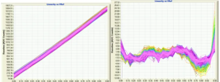
DC sweep of the channels input voltage is performed thanks to the possibility of fixing the baseline DC level via a DAC on the board. It permits DC transfer functions measurement of all the cells of all the channels of the chip as illustrated by the left plot of Fig.13.
Fig. 13. Left: ADC linearity calibration plot for all the cells from all the channels of a SAMPIC chip. Right: residues to a 2nd degree polynomial fit of the data from the left plot.
2.5 1.0 1.8 16 0 2 4 6 8 10 12 14 Cell 64 0 2 4 6 8 10 12 14 16 18 20 22 24 26 28 30 32 34 36 38 40 42 44 46 48 50 52 54 56 58 60 62
The cell-to-cell spread of slopes is of the with a random distribution (not related to c peak integral non-linearity is of 3%. B systematic and due to charge injection by sw be easily corrected after calibration. For this p same measurements, an individual cell fit is can be either a linear fit or a 2nd degree polyn parameters are used automatically by the so data during or after acquisition. The residues polynomial fits of the transfer functions from shown on the right are plotted on Fig. 13.
Without any linearity or gain spread corre would be degraded to ~7-8 bits RMS that c for most timing applications.
E. Discriminator
As the SAMPIC chip is mainly designed trigger, it is important to characterize its trig this purpose, a 3.1 kHz repetition rate, 150 m wide positive pulses are sent to the input of on baseline is fixed to 390 mV.
The detected rate is plotted as a f discriminator threshold set by the internal D in Fig. 14.
Fig. 14: detected hit rate as a function of the thresh wide pulses with 3.1 kHz pulses. The baseline was s threshold sweep up to 500 mV with the rate in logarithm on the region of the signal.
On the left plot of this figure, in logarithmic that the rate first increases then decrease corresponding to the baseline, before reaching of the signal. On this plot, we can see it is trigger reliably for threshold ~10 mV above th a plateau, the rate decreases for thresholds the signal amplitude, as seen by the discrimin fast pulse used, because of the limited b discriminator, the threshold corresponding to is only of 100 mV. This region of the plot is linear scale, on the right plot of Fig. 13. I standard S-curve usually used to characteriz By fitting this characteristic using an erfc extract a discriminator noise of 2 mV RMS i set internally, increased to 8 mV RMS if th externally. The reason for this higher no threshold is still being investigated, but the n of the chip is with internal threshold. We can mV RMS noise measured for the discrimina with the minimum detection level of 10 mV first part of the plot.
order or 1% rms channel). Peak to Both effects are witches. They can
purpose, from the performed which nomial one, which oftware to correct
s for a 2nd degree m the left plot is ection, resolution can be acceptable
to operate in self gering chain. For mV amplitude, 1ns ne channel which function of the DAC or externally hold for 150 mV, 1ns set to 390 mV. Left: mic scale. Right: Zoom
scale, we can see es for thresholds
g the 3.1 kHz rate possible to self-he baseline. After
corresponding to nator. For the very bandwidth of the o a 150mV pulse s zoomed, using a It is actually the ze discriminators. function, we can if the threshold is e threshold is set oise for external nominal operation
n notice that the 2 ator is consistent measured on the
F. Bandwidth and signal quality
Signal quality is highlighted by th 350 MHz sinewave (0.5 V peak-pea is a ‘out of the box’ single shot reco sole ADC linearity correction.
Fig. 15: raw 350 MHz sinewave sampled
As one can notice, all of the 64 d the signal already looks very good.
Fig. 16. Left: Frequency response of SA channels (smaller than 1%).
Fig. 16 shows the frequency resp with sinewaves similar to the on bandwidth is in the order of 1. expectations. It is constant all over memory. Ringing effects are prob impedance matching at the board inp The right plot of Fig. 16 shows channels is smaller than ±1%. VIII. TIME PERFORMANCES
A. Time resolution
In order to estimate the resolution we use a high-end generator, provid with 2.5 ns distance, 300 ps risetim peak, sent on 2 channels of a Sam shown in Fig. 17, are recorded in
he 64 samples taken on the ak) shown in Fig. 15. This orded @ 6.4 GS/s, with the
at 6.4 GS/s.
data points are usable, and
MPIC. Left: crosstalk between 2
ponse of the chip measured ne of Fig. 15. The -3dB
.6 GHz, close from our the 64 cells of the analog bably due to problem of put.
that the crosstalk between
n of the time measurement, ding after splitting, 2 pulses me, 1 ns FWHM, 800 mV mPic0 chip. The 2 pulses, n self-trigger mode at 6.4
GS/s, 11-bit mode, but the measured tim remain unchanged for sampling frequencies u
Fig. 17: the two pulses recorded at 6.4 GS/s (160 p timing measurements as recorded by SamPic0.
After non-linearity and pedestal common timing for each pulse is calculated online usi algorithm and interpolation as described in [8 The time differences distributions mea conditions are shown in Fig. 18. Without any we already get 18 ps RMS for Time Diffe (TDR), which is already at the level of the be corrected) TDC and sufficient for a lot of app
Fig. 18. Left: Δt timing distribution without any timi rms. Right: Δt timing distribution after TINL correction
We know from previous work that th distribution is mainly due to the spread of called Time integral non-linearity or TINL) that it can be easily calibrated and reliably c purpose, we have used the method described amplitude of segment of sinewaves crossing permits a very fast calibration procedure.
Once the TINL correction is simply ap becomes as good as 3.6 ps RMS. Looking which all events are plotted, one can not neither tail in the distributions, nor hit “out metastabilities, also no problem of boundarie validating then the “three ranges” architecture
ming performance up to 10 GS/s.
ps / sample) used for
n correction, the ing a digital CFD ] or [9]. asured in these y time correction, erence Resolution est (calibrated and plications.
ing correction ~ 18 ps ~ 3.5 ps rms.
his non-Gaussian f the delays (also
in the DLL and orrected. For this d in [8] using the g the origins that pplied, the TDR g at the plots, on tice that there is t of time” due to es between ranges
e of SAMPIC.
B. Time measurement as a function
The dependency of the TDR on t using two setups. To generate sm cable between the splitter and one o larger cable delays, this method i amplitude of the delayed signal di increases, both effect affecting the VIII.C. However, as shown in Fig from 2.7 ps RMS to 4.5 ps RMS fo this value, the TDR remains flat.
Fig. 19: time difference resolution vs delay
The shape of this characteristic ca on mind that at 6.4 GS/s the total DL a delay of 0 ns, the two pulses are DLL cycle. For delays larger than during different DLL cycles, so tha and the phase comparator are now values the probability to record th different DLL cycles is proportion consequently the progressive increas
As shown in Fig. 19, similar resu SAMPIC chips from different mezz two chips don’t share the same DLL on the two pulses are uncorrelated the single pulse resolution is better after TINL correction. For the meas we can notice a slight increase of delays. This tiny effect was only no shown here) when using a sim behaviour is mainly related to the d two-chip measurements (slower g risetime, 2-ns FWHM pulses, and reduces the signal slope and thus in electronics noise as shown on Fig 22
As shown in Fig. 20, the input quality of the timing measuremen MHz.
n of the delay and the rate
the delay has been studied all delays we introduce a f the SAMPIC’s input. For s no more usable, as the iminishes and its risetime e TDR as shown later in g. 19, the latter increases r delays up to 10 ns. After
y made by cables.
an be explained if we keep LL duration is of 10ns. For recorded during the same n 10 ns, they are captured at the jitters from the clock w added. For intermediate he two pulses within two nal to the delay explaining
se of the resolution. ults are obtained using two zanines. In this case, as the L, the timing measurements so that we can claim that than 3.2 ps RMS (4.5/√2) surements using two chips, f the TDR for the largest ticed for larger delays (not mple chip. The different
different setup used for the enerator providing 0.8-ns d different cables, which ntroduces extra jitter due to
2).
t rate does not affect the nt, event for rates of few
Fig. 20: measured time difference and TDR vs input h 400 ps risetime, 700 mV amplitude, and 7.1 ns delay puls
For larger delays we repeat the test using by two channels of a Tektronix AFG 325 Waveform Generator (AWG). The 800 mV, 2 ns FWHM, test pulses are slower than the p can be delayed digitally up to 10 µs. As show measured TDR is constant and better than 10 whole measurement range. This corresponds full range and is far better than the 100 ps ji the AWG. Moreover, on the whole 10 µs difference between the programmed and me within +/-15 ps (+/- 1.5 ppm), better tha specified for the AWG and showing a struct to the AWG internal design.
Fig. 21: Difference between the time measured using programmed on the AWG and TDR as a function of th long delays.
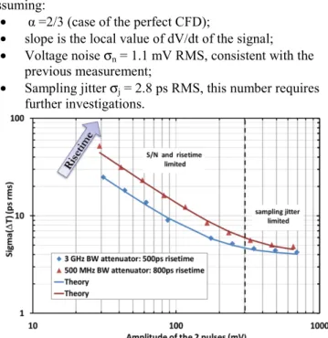
C. Timing Precision as a function of the amp
The TDR variation as function of the puls risetime is plotted in Fig. 22. For this meas FWHM pulse is attenuated before being sp SAMPIC channels. Two kinds of attenuato bandwidths have been used providing pulses respectively 500 and 800 ps. The measureme within very good agreement with the theore (lines) given by (1) which is the quadratic s term (sampling jitter) with a contribution pr signal risetime divided by its signal over noise
hit rate (1 ns FWHM, ses.
signals provided 52 [10] Arbitrary 2.5-ns risetime, 4-previous ones but wn in Fig. 21, the ps RMS over the s to 1 ppm of the itter specified for delay range the easured delays is an the precision ture probably due
SAMPIC and the one he time difference for
plitude
se amplitude and surement, a 2
ns-plit towards two or, with different with risetimes of ents (symbols) are etical expectation sum of a constant roportional to the e [11]. ∆ √ assuming:
• α =2/3 (case of the perfect CF • slope is the local value of dV/ • Voltage noise σn = 1.1 mV RM
previous measurement; • Sampling jitter σj = 2.8 ps RM
further investigations.
Fig. 22: Variation of TDR with the am different risetimes. The symbols are for corresponding to a fit using the quadratic sum
For both attenuators, the measure RMS for amplitudes larger than 10 one a TDR better than 20 ps RM pulses as small as 40 mV.
IX. SUMMARY OF PERFORMANCES Table I: Main features and measured p
Table I summarizes the main feat the SAMPIC0 chip.
X. CONCLUSION AND FUTURE DEVE
We have developed a multi-cha system (ASIC, boards, software measurement using the new WT
(1) FD);
/dt of the signal; MS, consistent with the MS, this number requires
mplitude of the pulses for two r measurements, the lines are m model.
ed TDR is better than 15 ps 00mV and with the faster MS is already reached for
performance of SAMPIC0
tures and performances of
ELOPMENTS
annel scalable acquisition e) for picosecond time
Digital Converter) concept integrated in the new SAMPIC ASIC.
The module works with even better performance than expected:
• 1.6 GHz Bandwidth; • Up to 10 GS/s;
• Low noise (trigger and acquisition); • << 5ps rms single pulse timing resolution.
It already meets our initial requirements, and is already usable for tests with detectors. Further work is ongoing on:
• Readout (firmware + software) optimization; • Fine characterization of this first prototype; • Characterization with fast detectors;
• A second prototype submitted in December 2014 on which the bugs detected on SAMPIC0 have been fixed and few minor improvements performed.
ACKNOWLEDGMENTS
This work has been funded by the P2IO LabEx (ANR-10-LABX-0038) in the framework "Investissements d’Avenir" (ANR-11-IDEX-0003-01) managed by the French National Research Agency (ANR).
We thank the team from TIMA/CMP Grenoble (France) for their precious contribution in providing access to MPW projects in AMS technologies.
REFERENCES
[1] J-F. Genat, G. Varner, F. Tang, H.J. Frisch, “Signal Processing for Pico-second Resolution Timing Measurements", Nucl. Instr. Meth. A 607 (2009) 387-393.
[2] D. Breton, E. Delagnes, J. Maalmi, K. Nishimura, L.L. Ruckman, G. Varner, J. Va'vra, “High Resolution Photon Timing with MCP-PMTs: A Comparison of Commercial Constant Franction Discriminator (CFD) with ASIC-based waveform digitizers TARGET and WaveCatcher", Nucl. Instr. Meth A 629 (2011) 123-132.
[3] D. Breton, E. Delagnes, J.Maalmi, P.Rusquart, “The WaveCatcher family of SCA-based 12-bit 3.2-GS/s fast digitizers”, submitted for publication in proceedings of IEEE RT 2014.
[4] E. Oberla et al., “A 15 GSa/s, 1.5 GHz bandwidth waveform digitizing ASIC”, Nucl. Instrum. Meth. A 735 (2014), p452.
[5] G.S. Varner et al., “The large analog bandwidth recorder and digitizer with ordered readout (LABRADOR) ASIC”, Nucl.Instrum.Meth.A583 (2007), p447.
[6] S. Ritt, “The DRS chip: Cheap waveform digitizing in the GHz range “, Nucl. Instrum. Meth. A 518 (2004), p470.
[7] E. Delagnes et al., “SAM: A new GHz sampling ASIC for the HESS-II front-end electronics”, Nucl. Instrum. Meth. A 567 (2006), p21. [8] D. Breton et al., “Picosecond time measurement using ultra-fast analog
memories” Proc. of TWEPP-09, Paris, France, p149 (2009).
[9] <E. Delagnes, http://irfu.cea.fr/Phocea/file.php?class=cours&file=/eric.delagnes/ED_W
aveform_digitizers_Valencia.pdf>, (2011). [10] http://www.tek.com/datasheet/afg3000-series, (2014). [11] E. Delagnes, Irfu internal note, (2014).