The AlInP Material System in Heterojunction Bipolar Transistor Technology
byAyqa Yiiksel
Submitted to the Department of Electrical Engineering and Computer Science in partial fulfillment of the requirements for the degrees of
Bachelor of Science
and
Master of Science at the
MASSACHUSETTS INSTITUTE OF TECHNOLOGY January, 1994
© Ayqa Yilksel, 1994. All rights reserved.
The author hereby grants to MIT permission to reproduce and to distribute copies of this thesis document in whole or in part.
Author...
...
.
. .-
...
...
Department of Electri al Engineering and Computer Science January, 1994
Certified by... .- - .. . ... Leslie A. Kolodziejski
/ AAssociate Professor of Electrical Engineering Thesis Supervisor
C ertified by ...
William U. Liu Texas Instruments, Inc. Thesis Supervisor
A ccepted by... ... .. .. . . ... ...
Frederic R. Morgenthaler Ch , EECS Committee on Graduate Students
t•
MVASS'ACN!US"T,3NST!rU'-;Ft: + ir.:Y~ (·
The AlInP Material System in Heterojunction Bipolar Transistor Technology
by
Ayqa Yiiksel
Submitted to the Department of Electrical Engineering and Computer Science on January 31, 1994, in partial fulfillment of the
requirements for the degrees of Bachelor of Science
and Master of Science
Abstract
An experimental study was carried out to investigate the use of the AInP material system in heterojunction bipolar transistor (HBT) technology. This thesis reports the first known d. c. and microwave performance of an AllInP/GaAs HBT. At an operating current density of 4.0 x 10⁴ A/cm2, the measured cutoff frequency and the maximum oscillation frequency are 20 GHz and 24.4 GHz, respectively. These high frequency results are respectable considering that the base doping used in the present design is only moderate at a value of 1 x 1019 cm-3. In addition, a preliminary passivation experiment and high temperature performance experiment were also conducted on these HBTs.
D. C. performance results of AIInP/GaInP and AllnP/AlGaAs HBTs are presented as well. The
current gains were 2 and 4, respectively, for these devices. Tests on GaInP/GaAs and A1GaAs/GaAs HBTs were also conducted for comparison. Current gains of 440 and 70 were reported for these devices. The poor performance of the AlInP/GaInP and AlInP/AlGaAs devices is attributed to a combination of staggered band lineup at the heterointerface and short minority carrier lifetimes in the base region of the transistors.
Thesis Supervisor: Leslie A. Kolodziejski
Title: Associate Professor of Electrical Engineering
Company Thesis Supervisor: William U. Liu
Acknowledgments
Any words of thanks are an insufficient expression of my gratitude to the people mentioned in this acknowledgment. I hope that you, and they, will keep this in mind when reading the following section.
First, I want to thank Dr. William Liu for his patience and guidance throughout my time at Texas Instruments. His support and technical knowledge has made this thesis possible.
I am also thankful to Dr. Darrell Hill, whom I consider my "surrogate supervisor". He gave very generously of his time and efforts, especially during my last work period at T. I.
I am grateful to Dr. Dean Collins, who gave me the opportunity to work at T. I. as a part of the VI-A program. This experience has been an invaluable part of my education at MIT.
This work has also benefited greatly from the knowledge and friendships of Terry Session, Jean Ramzel, Wanda Johnson, and Pat Tackett.
In addition, I want to thank Professor Leslie Kolodziejski who guided me in my research and made sure things ran smoothly for me at MIT. Her encouragement and criticisms were a very important contribution, not only to this work but also to my UROP experiences at MIT.
Last, but certainly not least, I must thank Orin Percus for calling me the night before my presentation; Janice Yoo for e-mailing me whenever she could, and Laura Bonner for hunting me down by phone when I moved two offices away. I have collected thirteen years of great experiences and memories between these three people. Their friendship is an inseparable part of who I am, and what I want to be.
A. Y.
Contents
L ist of Figures...
6
List of T ables...
...
9
List of Sym bols...
...
10
Introduction ...
13
1
Background
1.1 Sem iconductor D evice Theory... ... 141.1.1 Homojunction Bipolar Transistors... ... 15
1.1.2 H eterojunction Bipolar Transistors... 19
1.1.2.1 Base Current... ... 20
1.2 D . C. Characterization... ... 21
1.2.1 Ideality Factor... ... 21
1.2.2 Current-Voltage (I-V) Curve for an HBT... .... 23
1.2.3 D iode Characteristics. ... 24
2
Device Fabrication
2.1 Design... ... 25 2.2 Fabrication... ... 28 2.2.1 D. C. Process... ... 29 2.2.1.1 Em itter... ... 29 2.2.1.2 Base... ... 31 2.2.1.3 Collector... 38 2.2.2 R. F. Process... ... 39 2.3 Sum m ary... ... 453
Device Performance
3.1 AllnP/GaAs Npn HBT...49 3.2 AIlnP/GaInP and AIInP/A1GaAs HBTs... ... 51
4
Comparison of Different Material Systems
4.1 GaInP/GaAs and AIGaAs/GaAs HBTs...57 4.2 Passivation... ... 61 4.3 Temperature Dependance of Current Gain in AIInP/GaAs,
AIInP/GaInP, and AIInP/A1GaAs HBTs...64
Conclusions... 69
List of Figures
Figure 1.1 The schematic device structures of pnp and npn
transistors and their corresponding circuit elements ... 15
Figure 1.2 Equivalent circuit model of an npn transistor... ... 15
Figure 1.3 (a) Common-base, (b) Common-collector, and (c)
Common-emitter circuit configurations for the
bipolar transistor... ... 16
Figure 1.4 Simplified band-diagram for a transistor under (a) equilibrium
and (b) forward biased conditions...16
Figure 1.5 Simplified band diagram for a single heterojunction bipolar
transistor ... ... 19 Figure 1.6 Base current components: Ibr, Ire, Icont, and Isurf, of a
typical H BT... ... ... 20
Figure 1.7 Sample Gummel Plot used in measurement of ideality factors of
collector and base currents of a transistor... ... 22 Figure 1.8 Current-Voltage characteristics of an (a) ideal and (b) non-ideal
transistor showing regions of operation and variables of interest...23
Figure 2.1 HBT cross-section of an (a) passivated device and (b) non-passivated
device. (Note: not drawn to scale)... 26
Figure 2.2 A typical d. c. Npn epitaxial layer structure...27
Figure 2.3 (a) Mask pattern of a 100x100 gm2 d. c. HBT and
(b) SEM micrograph of the actual device... ... 29-30 Figure 2.4 Develop photoresist... ... 31
Figure 2.5 Evaporate ohmic m etal... ... 31
Figure 2.6 Com pleted em itter contact... ... 31
Figure 2.7 H2SO4:H202:H20 etch to active emitter layer...32
Figure 2.8 H3PO4:HC1 etch to base layer... ... 32
Figure 2.9 SEM images of resultant etches to the base layer of AIInP/GaAs and GaInP/G aA s HBTs... ... 33
Figure 2.10 Com pleted base contact... ... 37
Figure 2.11 Develop photoresist... ... 38
Figure 2.12 H2SO4:H202:H20 etch to subcollector layer... 39
Figure 2.13 Cross-section of a completed d. c. Npn HBT... ... 39
Figure 2.14 SEM image of a two-finger microwave HBT... 41
Figure 2.15 Schematic picture of a typical two-finger microwave HBT...42
Figure 2.16 R. F. processing sequence... ... 43
Figure 3.1 Ic-Vce characteristics of an AlInP/GaAs Npn HBT... .... 48
Figure 3.2 Gummel Plot of an AllnP/GaAs HBT...48
Figure 3.3 Measured current-gain values of a two-finger microwave device having a total emitter area of 2x60
pm
2 and a big device having an area of 100x100 pm 2... .. ... ... .. ... ... ... .. ... ... .. ... ... ... . . 49Figure 3.4 High-frequency performance of the 2x60
pm
2 AIInP/GaAs device in the common-emitter configuration...50Figure 3.5 Simplified energy-band diagram for an AllnP/AlGaAs/GaAs HBT emphasizing the heterojunction at the base-collector interface...52
Figure 3.6 Ic-Vce characteristics and Gummel plots of the processed AlInP/GaInP (a), (b); and AlInP/AlGaAs (c), (d), transistors ... 54
Figure 3.7 Emitter-base band diagram in a typical HBT... ... 55
Figure 3.8 Staggered band diagram at the emitter-base junction of an HBT...55
Figure 4.1 Ic-Vce plots of (a) AlGaAs/GaAs and (b) GaInP/GaAs HBTs ... 58
Figure 4.2 (a) Gummel plot of GaInP/GaAs HBT and (b) Gummel Plot of an A lGaAs/GaA s HBT... ... 59
Figure 4.3 Current gains of all devices: AllInP/GaAs, AlInP/AlGaAs, AIInP/GaInP, GalnP/GaAs, and AlGaAs/GaAs HBTs processed for this investigation...60
Figure 4.4 Gummel plot of a passivated 4x20
pm
2 AlInP/GaAs device...61Figure 4.5 Current gain versus collector current density for an (a) passivated and (b) unpassivated AlInP/GaAs device...62
Figure 4.6 Temperature dependence of current gain in (a) GaInP/GaAs and
(b) A1GaAs/GaAs HBTs... 65
Figure 4.7 Temperature dependence of current gain in (a) AIlnP/GaAs, (b) AllnP/AlGaAs,
Summary of microwave and d. c. device fabrication...46 Transistor parameters measured from the devices fabricated
for this investigation... ... 60
List of Tables
Table 2.3 Table 4.1
List of Symbols
a base transport factor
P
common-emitter, short-circuit, current gainBVceo breakdown voltage
Cbc total base-collector capacitance of device
d depletion layer width
Dnb hole diffusion coefficient in the base
Dne electron diffusion coefficient in the emitter
Dpb hole diffusion coefficient in the base
Dpe hole diffusion coefficient in the emitter
Ef Fermi level under equilibrium conditions
Ef* Fermi level under non-equilibrium conditions
Eg energy gap
Ei intrinsic Fermi level
Es dielectric permittivity
Ev energy at ceiling of the valence band
fmax maximum oscillation frequency
fT cutoff frequency
7
emitter injection efficiencyGmax maximum available power gain
h21 small-signal current gain
TIb ideality factor of base current
1Ic ideality factor of collector current
Ibr bulk recombination current in the base region
Ic collector current
Iceo common-emitter leakage current
Icont interface recombination current at the base contact
le emitter current
Inc collector electron current
Ine emitter electron current
Ipb base hole current back-injected into the emitter
Ipe hole emitter current
Ire recombination current in the base-emitter depletion region
Isurf surface recombination current in the exposed base region
Jbr base bulk recombination current density (A/cm2)
Jc collector current density
Jre base-emitter space-charge region recombination current density (A/cm2)
k Boltzman constant
Ksurf surface recombination current (A/cm)
LE emitter length
Lnb electron diffusion length in the base
Lpe hole diffusion length in the emitter
n electron concentration
ni intrinsic electron concentration
nie intrinsic carrier concentration in the emitter
Nne electron concentration in the emitter
Npb hole concentration in the base
p hole concentration
Pi intrinsic hole concentration
q elementary charge
Rb base resistance
T temperature
zb base transit delay
zc collector transit delay
zcr collector charging delay
ze emitter charging delay
Teff total emitter-collector transit time
Tnb electron lifetime in the base
Vbe emitter-base voltage
Vce(on) offset voltage
Wb effective base width
WE emitter width
WL passivation ledge width
Xe effective emitter thickness
Introduction
Recently, GaInP/GaAs structures for Npn heterojunction transistors (HBTs) have received much attention over AlGaAs/GaAs structures, due to the large valence band discontinuity, AEv, of GaInP with respect to GaAs. Similarly, the AlInP/GaAs system is an interesting alternative. AllInP lattice-matched to GaAs is expected to have an even greater AEv than its GaInP counterpart. With a greater AEv in the emitter junction, less base current due to back-injection of holes from the base into the emitter is likely to occur. Therefore, the AIInP/GaAs system appears very promising for Npn HBT applications. This thesis presents the results of the first fabricated AIInP/GaAs Npn HBTs. In this investigation, d. c. current gains of
100 are reported. Microwave testing of the devices yield a cutoff frequency of 20 GHz. The
maximum oscillation frequency obtained from the maximum available gain is 24.4 GHz.
The following pages present the discussion of processing and testing of AllnP/GaAs and AlInP/GaInP HBTs. Chapter 1 begins with a description of measurement techniques employed and reviews some pertinent academic background. Chapter 2 discusses the steps followed in the fabrication of the devices, emphasizing the difficulties of etching emitter material and the differences between d. c. and microwave processes. Chapters 3 and 4 present the results obtained for AIInP/GaAs, AIInP/GaInP, AIInP/AlGaAs, A1GaAs/GaAs, and GaInP/GaAs HBTs and compares these five designs for fundamental differences in performance. The last section of this thesis summarizes the conclusions of this work.
Chapter 1
Background
The academic disciplines that are the foundation of much of the work in this thesis are reviewed in the following chapter. Basic semiconductor device physics is used to describe transistor operation and materials characterization. In addition, d. c. measurement techniques used in the preliminary materials and device testing are discussed.
1.1 Semiconductor Device Theory
An introductory course in semiconductor physics that includes concepts of dopants, lattices, carriers, drift, diffusion, recombination-generation, and p-n junctions is helpful in understanding some of the concepts provided here. For reference, see Michael Shur's Physics of
Semiconductor Devices (1990) or Robert Pierret's Semiconductor Fundamentals (1987). An extensive
background in transistor structure and operation theory, however, is not assumed. A brief review of the relevant material is presented. For further treatment of this subject matter, see Gerold Neudeck' s The Bipolar Junction Transistor (1989).
1.1.1 Homojunction Bipolar Transistors
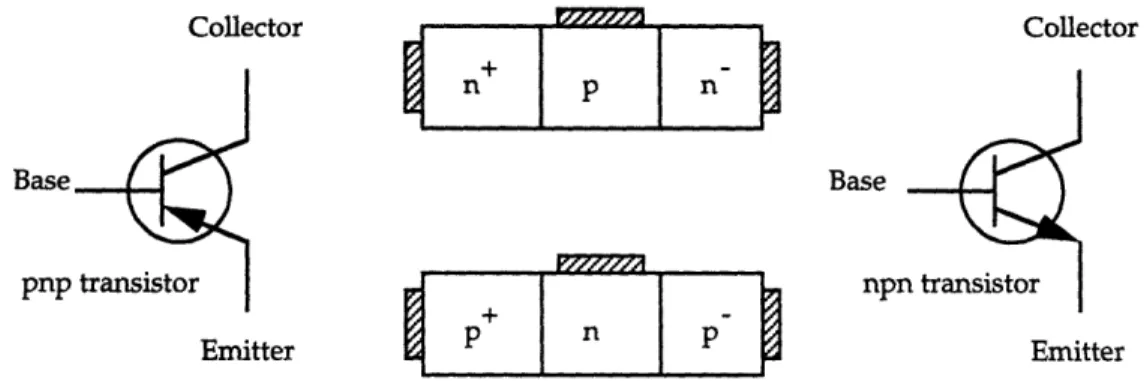
Homojunction Bipolar Transistors (BJTs) are three-terminal devices, fabricated from silicon and related oxides (as well as contact metals and silicides), that are used as amplifiers or logic elements. The schematic device structures of pnp and npn transistors along with their circuit elements are shown in Figure 1.1.
M777M
I
n
~
p
P771=~LP
n
p
Collector Base npn transistor Emitter Figure 1.1: The schematic device structures of pnp and npntransistors and their corresponding circuit elements.
Since the work of this thesis focuses primarily on npn transistors, only these will be discussed in further detail. As can be seen from Figure 1.1, a BJT is comprised of two back-to-back p-n junctions. An emitter region and base region form the first p-n junction. The second p-n junction is formed between the base and collector region. Since the base region is typically designed to be much shorter than the diffusion length of minority carriers in the base, these two junctions affect each other and are represented by the presence of controlled current sources in Figure 1.2.
emi ctor
base
Figure 1.2: Equivalent circuit model of an npn transistor
The minority carrier (electron in this case) diffusion length in the base, Lnb, for npn transistors equals fDnbZb, where Dnb is the electron diffusion coefficient in the p-type base and znb is the
minority carrier lifetime.
Collector
Base
pnp
Unlike field-effect transistors (FETs), which can only be modeled as common-source devices, there are three circuit configurations for the bipolar junction transistor. These are the common-base, common-emitter, and common-collector configurations, as shown in Figure 1.3.
C B B out B
inm
C E C E(a)
(b)
(c)
Figure 1.3: (a) Common-base, (b) Common-collector
and (c) Common-emitter circuit configurations for the bipolar transistor
Each has a power or current gain associated with it. The most widely employed configuration is that of common-emitter since this provides the narrowest band of frequencies over which the transistor is potentially unstable in high frequency applications. Consequently, the focus of this thesis also falls on the common-emitter configuration of transistors. Therefore, all references to measurements made regarding d. c. characteristics will assume this configuration.
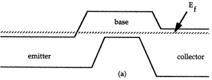
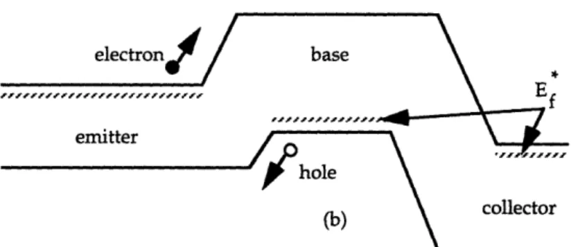
Under normal operating conditions of a BJT (forward active mode), the emitter-base junction (E-B junction) is forward biased, whereas the collector-base junction (C-B junction) is reverse biased. Qualitatively, the effects of biasing can be seen in the band diagram of the BJT. Figure 1.4 compares the band-diagram of a transistor under equilibrium (no bias) to that of
forward active mode.
Ef base
(Figure 1.4 continued on next page)
electron
emitter
r hole
(b)collector
Figure 1.4: Simplified band-diagram for a transistor under (a) equilibrium and (b) forward biased conditions.
The Fermi-Energy or Fermi level, Ef, introduced in Figure 1.4 (a), is computed from carrier concentrations under equilibrium conditions through the following relations:
n=
n
iexp[(-
Ei)
andp = pi exp[(Ei -Ef)
Similarly, Ef* represents the Fermi level computed from carrier concentrations under nonequilibrium conditions. The Fermi energy is referred to in this thesis only in the context of qualitative analysis of band diagrams of processed devices.
As shown in Figure 1.1, the emitter region of a BJT always has the highest doping. The collector region is doped the lowest. The base region has a doping level smaller than that in the emitter region but higher than that in the collector region. Since a transistor is often used as an amplifier or logic element, the reason for such a choice of doping levels is due to the desire for a current gain greater than unity for successful device performance. The desired effect of a large current gain, therefore, is achieved through the implementation of doping profiles and concentrations similar to those qualitatively represented here. Current gain occurs because electrons are injected from the emitter region, through the base, into the collector region, where the voltage drop is large compared with a small forward emitter-base voltage. The details of device design are presented later.
To date, extensive research has been conducted on silicon transistors and current gains of
1000 have been typically reported. However, GaAs, with its superior electrical properties and
versatility in doping design is also unmatched in Si BJT technology. The resulting impact of the addition of III-V materials on transistor technology is discussed in the next section.
As can be seen from the band diagram of Figure 1.4 (b), there exists another base-emitter current component in BJTs. Composed of holes from the base which are back-injected into the emitter, this current is substantial because both the holes and the electrons experience equal energy barriers at this junction. This is a property of the homojunction. The resultant back-injected current reduces the current gain of the transistor. To minimize this undesirable effect, therefore, the emitter must be more heavily doped than the base. This can be understood from the following equation, which formulates the ratio of desired electron injection current, In, from
the emitter to the base, over the undesired hole back-injection current, Ip, from the base to the emitter:
L D, Ne Le ne2
I,
Dpe Npb
Wb
ie
where D, N, L, and ni are diffusion coefficients, doping concentration, diffusion length, and intrinsic carrier concentration, respectively and the subscripts p, n, e, and b stand for holes, electrons, emitter, and base, respectively. Wb is the effective base thickness which is assumed to be less than Ln, the electron diffusion length in the base. As a result of different doping levels, there is greater injection of electrons from the emitter into the base than back-injection of holes from the base into the emitter, allowing for current gain,
0,
to be greater than unity. Quantitatively, current gain is defined as:I
c
D
neNne,
eexp(jEg
Ib
Dpb
NpbWb
kT
where AEg is the energy band discontinuity and Xe is the effective emitter thickness. When the emitter doping levels are increased, i.e. Nne is raised,
0
also increases. However, in practical devices, one must also consider the effects of very high doping levels which lead to changes in material parameters, in particular, to a decrease in the energy gap. Consequently, an exponential AEg dependence is also included in the definition ofP
for this reason.Emitter injection efficiency, y, is another performance parameter used in evaluating device quality. y measures the ratio of injected electron current to total emitter current:
I I
le
(Ine + IpeNote that y -- 1 if Ipe -4 0. That is, as the emitter is more heavily doped, Ipe becomes a smaller percentage of Ie. For large-gain transistors, y is made as close to unity as possible.
The design constraint on the emitter of a BJT severely restrains variations on device design in homojunction transistor technology. Specifically, doping and
0
cannot be varied independently.1.1.2 Heterojunction Bipolar Transistors
As a result of the limitations that BJT technology imposes on emitter design,
heterojunction bipolar transistors (HBTs) have been developed. Fabricated from III-V
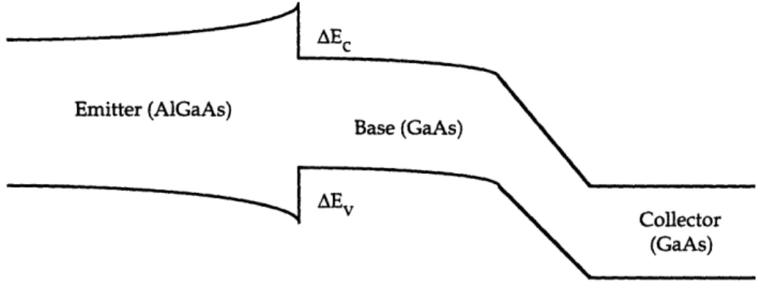
compounds such as AlAs and GaAs, a typical HBT has an emitter region made of a different material which has a larger bandgap than the rest of the device. This allows for an additional freedom in choosing doping densities of the emitter and base layers. Consequently, with the use of higher base doping, the HBT has lower base resistance and E-B junction capacitance, giving it a significant speed advantage over BJTs. The resulting band diagram is shown in Figure 1.5.
AEv
Collector
(GaAs)
Figure 1.5: Simplified band diagram for a single heterojunction bipolar transistor.
As a result of the abrupt heterojunction, 0 is also modified to:
D, Nne
Xe1exp(
Ev
[D,
Npb Wb kT1.1.2.1 Base Current
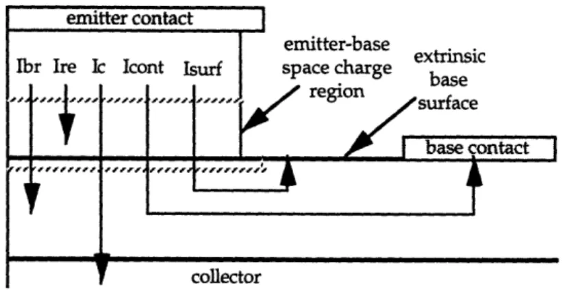
Because of the use of a different emitter material which drastically reduces back-injection of minority carriers from base to emitter, other components of base current emerge. There are four major base current components of the HBTs under consideration: (i) surface recombination current in the exposed base region (Isurf); (ii) interface recombination current at the base contact (Icont); (iii) bulk recombination current in the base region (Ibr); and (iv) recombination current in the base-emitter depletion region (Ire). These current components are also illustrated in Figure
1.6.
For the first component, one should note that the surface recombination velocity of GaAs has been found to be relatively high. Since this material is widely used in HBT technology as the base material, it is important to take its surface characteristic into consideration. Because of the high surface recombination velocity on the extrinsic base surface, many minority carriers injected from the emitter recombine with the base majority carriers at this surface. Base contact recombination current is due, again, to a high interface recombination velocity. However, if the base and emitter contact separation is large, then most carriers from the emitter simply cross the base and reach the collector without diffusing to the base contact and recombining there. The third component, Ibr, exists because of the presence of bulk recombination traps. If the base is excessively thick, most minority carriers recombine in the base before reaching the collector. Finally, Ire, is B space charge (depletion) region recombination current. In the forward-bias E-B junction, a lowered electrostatic potential barrier allows for high concentrations of electrons and holes to diffuse from the neutral base and emitter regions into the depletion region. Because of increased carriers, significant recombination occurs in this region.
emitter contact
emitter-base extrinsic
Ibr Ire Ic Icont Isurf space charge h,,
r
region surface
base contact
collector
Figure 1.6: Base current components: Ibr, Ire, Icont, and Isurf, of a typical HBT.
I
1"1
rrr~/rI
I
Vabr-Now, d.c. current gain is limited primarily by these recombination currents:
I I
P= = Ine
Ib (Ire+ Ibr+ Icont+ Isurf)
As suggested by the above descriptions, the reduction of most of these components of the base current can be accomplished through device design. HBTs, to date, have been fabricated with
A1GaAs/GaAs and GaInP/GaAs as emitter/base material. This thesis also investigates
AlInP/GaAs and AlInP/GaInP as possible additions to the combinations of III-V materials suitable for semiconductor applications. The methods of device performance evaluation are
discussed in the next section.
1.2 D. C. Characterization
In the d. c. characterization of bipolar transistors, one of the most important parameters is the d. c. current gain, p. Therefore, the analysis of various factors affecting
P
is the primary concern of this paper. The tools used in this analysis; current-voltage curves, Gummel plots, and p-n junction diode characteristics, as well as the variables under question: P, leakage current, and the ideality factor, will be summarized here.1.2.1 Ideality Factor
Ibulk and Isurf, as noted before, result from intrinsic bulk and extrinsic surface recombination, respectively. It is important to determine which of these components dominates the base current of a transistor in order to optimize the device's performance. In general, knowledge of the ideality factor of various current components as a function of base-emitter voltage, Vbe, and temperature enables one to better understand and interpret the experimental
results.
The ideality factor, 71, of a current can be derived from the current-voltage relationship of the transistor. Quantitatively, 11c and 1b are ideality factors of the collector and base currents, respectively, and are related to the currents as shown in the following equations:
ic: Ic= Ico expa qVbe
(,Ic k T and
11b: Ib= Iboexp qVbe
ýýbkT)
Experimental results have shown that ilc ~ 1 for a graded1 E-B junction HBT, - 1.1 for an abrupt2
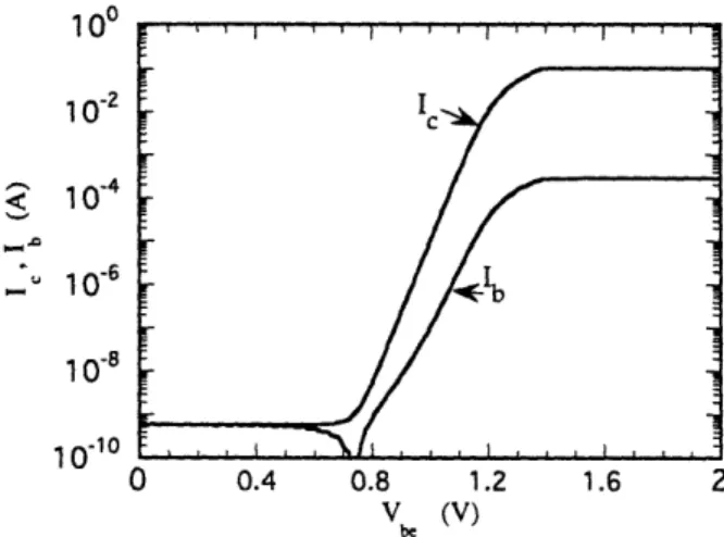
junction HBT, and -1.3 for a junction with InP material.3 Experimental and theoretical evidence also show that Tlb= 1 for Ibulk, 2 for Ire and 1 for Isurf. 4,5 The ideality factor can readily be deduced from Ic and Ib versus Vbe curves showing collector and base current with respect to E-B junction bias (Vbe). A sample plot is shown in Figure 1.7. This plot is called a Gummel plot and the areas of linearity of the currents mark the range of Vbe bias for which the ideality factor is of concern. The base-collector bias, Vbc, is kept at zero for these measurements.
100 10-2 10-4 10-6 10.8 10-10 0 0.4 0.8 1.2 V (V)be 1.6 2
Figure 1.7: Sample Gummel Plot used in measurement of ideality factors of collector and base currents of a transistor.
1 refers to devices with a gradual variation of aluminum composition over the base-emitter junction (typically AlGaAs emitter and GaAs base).
2 refers to devices where the aluminum composition in the entire emitter (typically A1GaAs)
remains unchanged.
3 "Current Transport Mechanism in GaInP/GaAs Heterojunction Bipolar Transistors," W. Liu,
S. Fan, T. Kim, E. Beam, D. Davito. IEEE Transactions on Electron Devices, vol. 40, no. 8. August 1993.
4 "Diode Ideality Factor for Surface Recombination Current in A1GaAs/GaAs Heterojunction Bipolar Transistors," W. Liu, J. Harris, Jr. IEEE Transactions on Electron Devices, vol. 39, no. 12. December 1992.
5 "Extrinsic Base Surface Passivation in GaInP/GaAs Heterojunction Bipolar Transistors," W. Liu, E. Beam, T. Henderson, S. Fan, IEEE Electron Device Letters, vol. 14, no. 6. June 1993.
1.2.2 Current-Voltage (I-V) curve for an HBT
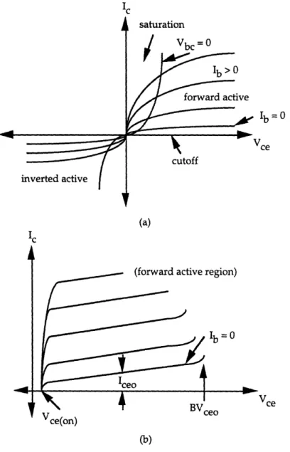
This section discusses the current-voltage (I-V) characteristics of a typical HBT. Figure 8 compares ideal and non-ideal I-V curves. As can be seen from these graphs, there are four regions of operation: cutoff, saturation, forward active, and inverted active. When compared to the ideal I-V curve of Figure 1.8 (a), the non-ideal curve (Figure 1.8 (b)) shows several interesting discrepancies. inverted active saturation
j
Vbc = 0
Ib = 0 Vce cutoff(forward active region)
/ Ib=0
BVceo Vce
cekon)
Figure 1.8: Current-Voltage characteristics of an (a) ideal and (b) nonideal transistor showing regions of operation and variables of interest.
First, the slope of the forward-active common-emitter non-ideal I-V curve is due to the generation current produced in the C-B depletion region. Electrons and holes are generated, each contributing to an increase in collector current (Ic) as the C-B depletion region increases under increased reverse bias. However, the largest increase is a result of the generated holes drifting into the base, where they become majority carriers. In the case of a microwave device, leakage current due to implantation damage is also of concern. The generated holes in the base-collector depletion region add directly to the back-injected holes at the E-B junction which forces a much larger increase in the injected electrons from the emitter which, in turn, diffuse to the collector junction and increase Ic significantly. At Ib = 0, this observed phenomenon is referred to as the collector-emitter leakage current, Iceo. Leakage current is an unwanted effect since it causes a
steady increase of current gain over the measured range of collector current. Ideally, one wants a constant current gain for a given range of Ic for reasons of reliability and reproducibility of transistor performance.
The common-emitter avalanching characteristic is also illustrated in Figure 1.8 (b) and is characterized by the second variable of interest, the breakdown voltage of collector-emitter, BVceo. This breakdown voltage is defined with the base open-circuited.
1.2.3 Diode characteristics
Lastly, each of the junctions, E-B and C-B, are p-n junction diodes. As discussed
previously, measurement of the I-V characteristics of the diodes can give valuable information on leakage current and turn-on voltage of the transistor. Typically, turn-on voltage for the emitter-base heterojunction is 1.1 - 1.2 V. The collector-base homojunction turns on at - 0.7 - 0.9 V. The
difference in turn-on of these two junctions results is an offset voltage of the same magnitude for the transistor. The offset voltage, Vce(on) is, in effect, the point at which the transistor begins to operate.
Chapter 2
Device Fabrication
The purpose of this chapter is to detail the methods of design and fabrication used in making the devices under investigation. The section on design gives some broad guidelines to consider when deciding upon doping densities and layer thicknesses. The section titled "Fabrication" describes the steps used in the actual processing of the transistors.
2.1 Design
In order to facilitate the methods of comparison, we adopt the same structures for AlInP/GaAs and AIInP/GaInP HBTs that are used in GaInP/GaAs and AlGaAs/GaAs material systems. The chosen doping levels of emitter, base, and collector, minimize bulk resistances while still yielding respectable values of current gain. The base region is designed to be much shorter than the diffusion length of the minority carriers in the base, thereby minimizing loss of carriers due to recombination. One of the most important design considerations is in the reduction of the base current components. Given the definitions of these components (section
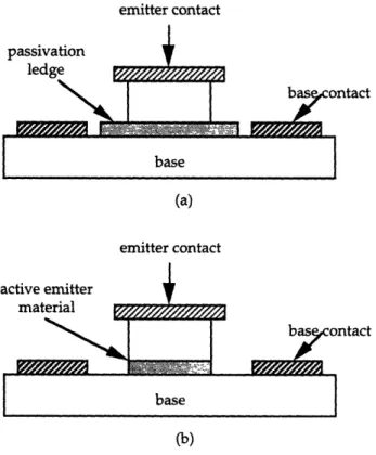
1.2.1), one can make certain preferences in the mask design or device structure. For example, Icont is reduced if the base-emitter contact separation is large (much longer than the base thickness). Then, most carriers from the emitter simply cross the base and reach the collector without diffusing to the base contact and recombining there. Ibr is also reduced if the base is designed to be thin so that a negligible number of carriers recombine in the base before reaching the collector. Finally, the extrinsic base surface recombination current is reduced through surface passivation with a depleted ledge composed of the active emitter material. Figure 2.1 compares an HBT structure with a passivation ledge (a) to one which has not been passivated (b).
emitter contact
ntact
emitter contact
mntact
Figure 2.1: HBT cross-section of (a) a passivated device and (b) non-passivated device. Shaded region indicates that the emitter is composed of different material than either the cap or base regions. (Note: not drawn to scale)
The passivated device has a ledge which is depleted due to the combination of the surface depletion region and the p-n junction depletion region. As a result, this depleted ledge reduces carriers at the surface which, otherwise, tend to recombine and, therefore, increase Ib. Optimal thicknesses of the ledges are dependent on the material used and have been experimentally
determined to be between 700-1000
A for AlGaAs and GaInP material.
3, 6, 7 Emitter, base, and collector doping levels are also determined by considering material resistivity. For example, base bulk recombination current increases with base doping due to the decrease in the minority carrier lifetime of the material as a result of recombination. For high frequency applications, however, a high base doping level is desired, as discussed in Chapter 3. Therefore, a compromise must bemade on the base doping in order to optimize transistor performance.
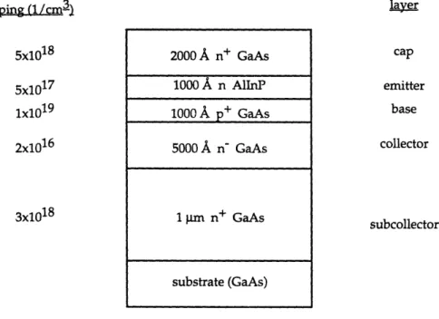
The basic structure of a device used in this investigation is illustrated in Figure 2.2.
doping (1/cm3) 5x101 8 5x10¹⁷
N119
1x101 2x10⁶ 3x101 8 layer cap emitter base collector subcollectorFigure 2.2: A typical d. c. Npn epitaxial layer structure
Cap and subcollector layers are doped higher to reduce contact resistance. In this investigation, the active emitter layer was also composed of AlGaAs or GaInP material. The base and collector layers are typically GaAs, although some devices with GaInP or A1GaAs base, and GaInP collector layers have also been processed for this study. For ease of comparison, the thicknesses and doping levels used are identical across all of the material systems used: AlGaAs/GaAs, GaInP/GaAs, AlInP/GaInP, AlInP/AlGaAs, and AllnP/GaAs. In addition, the device structure
6 Pnp Heterojunction Bipolar Transistors in AlGaAs/InGaAs/GaAs, D. Hill, Ph.D. Dissertation,
Stanford University, Stanford, CA, pp. 74-87. June 1990.
7 "Exttrinsic Base Surface Recombination Current in GaInP/GaAs Heterojunction Bipolar Transistors with near-Unity Ideality Factor", W. Liu, Jpn. J. Appl. Phys. vol 32, 1993, pp. 713-715.
2000 A n+ GaAs
1000~iAn AIInP
1000 A p+ GaAs 5000A
n- GaAs 1 pm n+ GaAs substrate (GaAs)employed here has been used extensively in the GaInP/GaAs and AlGaAs/GaAs material systems, yielding well-established and previously published results.
The HBT material was grown with metalorganic molecular beam epitaxy (MOMBE). Elemental Be and Sn were used for p and n type dopant sources, respectively. The Al source for AlInP was elemental aluminum evaporated from a conventional effusion cell. The AlInP layer was grown at 500° C at a growth rate of - 0.9
p•m/hr,
with a V:III ratio of less than five. In addition, elemental Ga and In sources were used for the GaAs, AlGaAs, and GaInP layers.8The principal test of material quality was device performance using the MOMBE grown layers of AllInP, GaInP, AlGaAs, and GaAs. The obtained results for the AlInP devices were compared to published reports on better known material systems of GaInP and GaAs. Consequently, the doping densities and layer thicknesses used in this investigation were borrowed from previously published work of GaInP and GaAs device structures in order to
facilitate comparisons between material systems. In the future, however, a thorough
investigation of the AIInP material system requires specific tests to assess the quality of the epilayers, such as Hall measurements to determine mobility, photoluminescence studies on lattice mismatch at the interface, X-ray diffraction measurements to observe variations in lattice constant versus film thickness, and double crystal X-ray diffraction rocking curves to study the effect of various parameters involved in film growth on the crystal structure of the epitaxial layers. Transmission electron microscopy (TEM), scanning electron microscopy (SEM), and high-resolution electron microscopy (HREM) can also be used to study the effects of lattica-mismatch and the subsequent dislocations found at the interface.
2.2 Fabrication
The device fabrication techniques described here are primarily those of the transistors made for d. c. characterization. Because one AIInP/GaAs wafer was also processed for high-frequency testing, however, this technique will also be discussed briefly.
8 The Use of Tertiarybutylphosphine and Tertiarybutylarsine for the Metalorganic Molecular
Beam Epitaxy of the InGaAs/InP and InGaP/GaAs Material Systems," E. A. Beam III, T. S. Henderson, and J. Y. Yang, Journal of Crystal Growth, vol 116, 1992, pp. 436-446.
2.2.1 D. C. Process
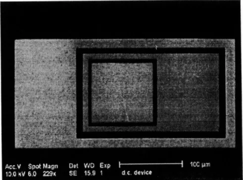
The mask design used (a) and a scanning electron microscope (SEM) micrograph (b) of the actual device are shown in Figure 2.3.
Figure 2.3: (a) Mask pattern of a 100x100 pm2 d. c. HBT.
The shaded region indicates areas with metal contacts.
This d. c. device is used in the preliminary testing of the material quality. The d. c. current gain,
P, measured from the device as well as its current-voltage characteristics, can give great insight
into the appropriateness of a given material system for use in transistor technology. The steps followed in processing each layer are given in the following sections.
2.2.1.1 Emitter
The emitter layer contact deposition begins with a solvent cleaning of the surface to remove residual dirt and grease. Next, photoresist is applied using a spin-on technique and exposed with the emitter mask pattern. In this case, photoresist was spun on the wafer at a rate of 3725 rpm for 20 seconds. The development time ranged from three to four minutes depending on exposure intensity used. Figure 2.4 illustrates the resultant profile after the photoresist is developed.
12190
emitter photoresist
cap
collector subcollector
Figure 2.4 Develop photoresist
emitter contact photoresist
cap emitter
ba~e collector subcollector
Figure 2.5: Evaporate ohmic metal
Next, AuGe/Ni/Au ohmic contacts are deposited on the surface (Figure 2.5); and the resist is lifted off with acetone. (Fig 2.6). Once the emitter contacts are evaporated, the wafer is ready for base layer process.
emitter
\-emitter contact cap haqe collector subcollectorFigure 2.6: Completed emitter contact
2.2.1.2 Base
The most difficult step involved in forming the base contact is the etch to the base layer. The emitter contacts are used as a natural mask pattern to wet-etch regions other than the emitter
mesa down to the base layer. Using previously published reports9 , 10 ,11, 12 on etchants as a guideline, the cap layer of GaAs is etched in a solution of H2SO4:H202:H20 to expose the active emitter material, as shown in Figure 2.7.
emitter contact emitter contact
a e m base collector Figure 2.7: H2SO4:H202:H20 etch to active emitter layer
collector
Figure 2.8 H3PO4:HCI etch to base layer.
Next, the active emitter material, AlInP, is etched. At this point, a dilute solution containing H3PO4 : HC1 or H20: HCI is used for AllInP. HCI also attacks GaInP, however, and if the emitter material is GaInP, a higher concentration of HCI in solution should be used to properly etch this layer. A 3:1, H3PO4 : HCI solution was used for GaInP, and a 30:1 H3PO4:HCI solution was used
for AllnP in this investigation. In the case of AlGaAs emitter material, an etchant containing H2SO4, H202, and H20 is used to etch through the emitter layer (Fig. 2.8). SEM micrographs of resultant etches to the base layer of AlInP/GaAs and GaInP/GaAs HBTs are shown in Fig. 2.9.
9 "Selective Wet Etching of GaInP, GaAs, & InP in Solutions of HC1, CH3COOH, and H202," J.
R. Flemish and K. A. Jones, J. Electrochem.Soc., vol. 140, no. 3. March 1993.
10 "Wet and Dry Etching Characteristics of AllInP," J. R. Lothian, J. M. Kuo, W. S. Hobson, E. Lane, F. Ren, and S. J. Pearton, J. Vac. Sci. Technol, B 10(3). May/June 1992.
11 "Etch Rates and Selectivities of Citric Acid / Hydrogen Peroxide on GaAs, A1GaAs, InGaAs, InA1As, and InP," G. C. DeSalvo, W. F. Tseng, J. Comas, J. Electrochem. Soc., vol. 139, no.3. March
1992.
12 "Plasma and Wet Chemical Etching of InGaP, "J. R. Lothian, J. M. Kuo, F. Ren, S. J. Pearton,
Journal of Electronic Materials, vol. 21, no.4. 1992.
active emitter
12193
Figure 2.9 (a): SEM micrograph of an emitter contact and etch to the base layer of a GaInP/GaAs HBT
12191
Figure 2.9 (b): SEM micrograph of the emitter contact and etch to the base layer of an AllnP/GaAs HBT
12791
Figure 2.9 (c): SEM image of GaInP profile etched in H3PO4:HCI
12792
Figure 2.9 (d): SEM image of a GaInP profile etched in H3PO4:HCI and cleaved along [011] crystal orientation. (Note: No cap layer of GaAs for this sample)
The SEM micrographs also emphasize the importance of contact pattern orientation with respect to the wafer since etch profiles change drastically for different planes of crystal geometry of the material in question.
In cases where the emitter material is either GaInP or AlInP, the process is described as a selective etch since the acids used to etch GaInP and AlInP stop at the GaAs base layer. This characteristic of the etchant is particularly useful if one has to etch to a very thin base layer and accidentally etching through the base becomes a concern. (Care must still be taken to time the etch properly in order to prevent excessive undercut of the emitter contacts.) This, however, is not the case for A1GaAs/GaAs HBTs where H2SO4:H202:H20 is used to etch through both the AlGaAs emitter layer and the GaAs base layer.
After the base contact etch, the base contact region is defined with the base mask pattern
by application of the resist using a spinner, exposure, and development. Finally, Ti/Pt/Au
contacts are evaporated on the surface. The resist is then lifted off. The result is illustrated in Figure 2.10.
emitter contact
bac cont
collector
2.2.1.3 Collector
Since the collector is of the same material as the base, and stopping the etch right at the subcollector layer is not an issue, collector contact lithography is a far simpler process. First, resist is applied using a spin-on technique, exposed, and developed. Then, the GaAs (or GaInP, depending on base material used) is etched through the base and the collector layers to the subcollector. In this case, since the collector contact covers the entire periphery of the emitter and base patterns (Figure 2.3), an etch with the resist pattern results in device isolation. Figure 2.11 shows a cross-section of the device after resist development.
photoresist
base
collector (GaAs)
subcollector (GaAs)
Figure 2.11: Develop photoresist
The etch rate is controlled through timing and concentration of solution and the etch depth is monitored through alpha-step measurements and probing of the surface breakdown voltage. The material is etched until the subcollector is reached because the subcollector is doped with a higher concentration than the collector, thereby reducing contact resistance. (Figure 2.12)
photoresist
subcollector (GaAs)
Figure 2.12: H2SO4:H202:H20 etch to subcollector layer
Finally, AuGe/Ni/Au contacts are evaporated and the resist is lifted off. As a final step in the process, the completed device is alloyed at 430' C in order to reduce contact resistances. A cross-section of a finished d. c. heterojunction bipolar transistor is shown in Figure 2.13.
cap layer (GaAs) activ
base (GaAs)
ve emitter layer
(AllnP)
subcollector (GaAs)
Figure 2.13: Cross-section of a completed d.c. Npn HBT
2.2.2 R. F. Process
The r. f. process differs from the d. c. process both in mask pattern used and method of isolation of devices. Importance is also given to the quality of contacts as one strives to minimize parasitic effects which tend to slow down device performance. Air bridges are used to connect collectors in multiple-finger devices.
Figure 2.14 shows an SEM image of a finished HBT. A schematic in Figure 2.15 of an microwave device helps to clarify the various parts of the transistor.
The first difference between r. f. and d. c. devices is in the mask pattern. For r. f. devices, the collector contact does not surround the emitter and base contacts. Therefore, other means must be employed in order to achieve device isolation. Ion implantation techniques are used for this purpose. Ions having high kinetic energies, are implanted into the surface and serve to disrupt the ordered lattice of the epitaxial layers, thereby creating a nonconducting barrier between devices. The consequences of this implantation, however, result in difficulties in etching the disordered surface areas, particularly in the GaInP active emitter layer.
Contact annealing is an additional step in the emitter process sequence of microwave devices. Heating contacts to temperatures above 2000 C after evaporation and liftoff improves the semiconductor and contact interface by increasing the diffusion of GaAs from the cap layer into the ohmic contact, thereby facilitating conduction across this interface.
Passivation of transistors is also a design consideration in small, r. f., devices. Specifically, extrinsic base surface recombination current is proportional to the length of the emitter periphery. For microwave devices in specific, the emitter width is 2 ntm or less, which is drastically smaller than the emitter length (- 30 Ium). Therefore, in unpassivated devices where
the extrinsic base surface recombination current is significant, the current gain decreases as the emitter area decreases. A study of current gain in these devices must take this design variable into consideration.
12194
Figure 2.15: Schematic picture of a typical two-finger microwave HBT © William Liu
The passivation ledge in a typical HBT, as shown in Figure 2.1, is the active emitter layer which extends as far as the base contacts. Normally, to contact the base, one must etch away this depleted AlInP layer to reach the p-type base layer. However, prior to indiscriminately etching all of this AlInP layer, a surface mask is used to protect a narrow depletion ledge which surrounds the emitter mesa and prevents it from being removed. Once the photoresist is defined to protect the not-to-be etched AIInP, a solution of H3PO4 : HCl is used to etch down to the base surface.
The process sequence for a microwave device is delineated in Figure 2.16. A description of each step is given in the caption following the illustration.
AuGe/Ni/Au
1. Use emitter mask to evaporate AuGe/Ni/Au emitter contacts.
Anneal at 430' C
base Ti/Pt/Au
\
1. T T / t A
2. Etch down to base. Evaporate Ti/Pt/Au base contacts.
collector
3. Use collector mask. Etch down to subcollector.
Evaporate AuGe/Ni/Au collector contacts. Anneal contacts.
nitride
4. Deposit Nitride nitride
collector
subcollector
5. Use photoresist and "Pads" mask to etch nitride around collector contacts
/mrs~s ~ ~zJ\ f
nitride air bridge
6. Evaporate Airbridge and liftoff resist.
Figure 2.16: R. F. processing sequence
2.3 Summary
Table 2.3 shows a summary of device fabrication, highlighting the differences in d. c. and r. f. process. The methods discussed in this chapter were used extensively in making the devices under investigation, the results of which are presented in the next section.
Layer D. C. Process
solvent clean spin photoresist
expose to "EMITTER" mask pattern
Emitter develop, inspect
bake
clean developed surface evaporate AuGe/Ni/Au contacts
liftoff
wet etch (H2S04:H202:H20)
to remove GaAs cap layer wet etch (H3PO4:HC1) to remove AIInP active emitter layer
spin photoresist
Base expose to "BASE" mask
pattern
develop, inspect clean surface
evaporate Ti/Pt/Au contacts liftoff
spin photoresist
expose to "COLLECTOR" mask pattern
develop, inspect
Collector clean surface
evaporate AuGe/Ni/Au contacts liftoff Alloy contacts at 430' C [DONE] PadsP Pads "' '1 Mk
tni X
· · ;7\:\·~&
7" R. F. Process solvent clean spin photoresistexpose to "EMITTER" mask pattern develop, inspect bake at 80' C, 3 minutes clean surface evaporate AuGe/Ni/Au contacts liftoff Alloy contacts at 430' C use a combination of H2SO4:H202:H20 and
reactive ion etching (RIE) techniques to remove cap and emitter material
spin photoresist expose to "BASE" mask pattern
develop, inspect clean surface
evaporate Ti/Pt/Au contacts liftoff spin photoresist expose to "COLLECTOR" mask pattern develop, inspect clean surface evaporate AuGe/Ni/Au contacts liftoff Alloy Contacts at 430" C spin photoresist
expose to "PAD" mask pattern develop, inspect
bake at 80" C, 3 minutes clean surface
evaporate Ti/Pt/Au pads liftoff, inspect spin photoresist expose to "AIRBRIDGE 1" mask pattern develop, inspect spin photoresist expose to "AIRBRIDGE 2" mask pattern develop, inspect plate surface with Au.
[DONE]
Table 2.3: Summary of microwave and d. c. device fabrication
..6 ... 9 ... ý- , - _ _
Chapter 3
Device Performance
This chapter describes the experimental results for the first reported Npn HBTs based on
the AlInP material system. Three distinct devices; AlInP/GaAs, AlInP/GaInP, and
AlInP/A1GaAs HBTs, were fabricated. Their performance results are discussed in the following sections. Chapter 4 presents a comparison of the AlInP material system with the better known material systems of GaInP and AlGaAs.
3.1 AlInP/GaAs Npn HBT
The epitaxial structure of this device is presented in Chapter 2. The d. c. characteristics of the fabricated HBTs were measured with a Semiconductor Parameter Analyzer and the current-voltage characteristics (Ic-Vce) are shown in Figure 3.1.
0 1 2 3 v (V)
4 5 6 7 Figure 3.1 Ic-Vce characteristics of an AllnP/GaAs Npn HBT
The common-emitter current gain of these devices is as high as 100 using an emitter area of 100
x 100 pm2. The breakdown voltage, BVceo, is - 6.5 V, consistent with the collector design used
for this study. The offset voltage, Vce(on), is approximately 0.4 V, a value that is in good agreement with the measurement of the base-emitter and base-collector junction diode characteristics.
A Gummel plot of the same device is shown in Figure 3.2.
10
-10-3
10 -10-9 0 0.4 0.8 1.2 V (V) 1.6 2Figure 3.2 Gummel plot of a d. c. and microwave AlInP/GaAs HBT
0.06 0.05 0.04 0.03 0.02 0.01 0
The ideality factor, rib, for the base current was measured at 1.48. The various components of base current have been presented in section 1.1.2.1. The surface recombination current is believed to be negligible for this device because of its large size. Therefore, the measured ilb = 1.48 indicates that the recombination currents in both the space-charge region and the base layer are equally important. For the collector current, ic is 1.13. This ideality factor deviating from unity for the abrupt AIInP/GaAs base-emitter junction indicates a significant
conduction-band discontinuity, AEc, in the AlInP/GaAs heterojunction. It has been previously
demonstrated in GaInP/GaAs HBTs that, if AEc is small, the collector current is limited by the transport through the base layer and exhibits a unity ideality factor13. Figure 3.2 also shows a Gummel plot of a 2 x 60 Cm2 microwave device. Measured ideality factors for collector and base currents, respectively, are 1.38 and 2.52. The increase in rib from d. c. to microwave device indicates that, because of the reduction in device size, the surface recombination currents both in the extrinsic base surface and implantation boundary are no longer negligible in the microwave transistor.
Figure 3.3 illustrates the measured current gain values of the two-finger microwave device having a total emitter area of 2 x 60 pm2 and a device having an area of 100 x 100
p.m
2.,I n, 3
10
102
" 101
1
Collector Current (A)
Figure 3.3: Measured current-gain values of a two-finger microwave device having a total emitter area of 2x60 im2 and a big device having an area of 100x100
pm
2.13 "Current Transport Mechanism in GaInP/GaAs Heterojunction Bipolar Transistors," W. Liu, S. Fan, T. Kim, E. Beam, and D. Davito, IEEE Transactions on Electron Devices, vol. 40, no.
In general, the relationship between the current gain,
13,
and the emitter dimension (emitter width: WE, emitter length: LE) can be expressed as:1 (Jbr +Jre) + 2Ksur
Jc
Jc 2WE +2LEwhere Jbr (A/cm2) and Jre (A/cm2) are the base bulk recombination current density and the base-emitter space-charge region recombination current density, respectively, and Ksurf (A/cm) is the surface recombination current divided by the emitter periphery.14 Because of the difference in their perimeter to area ratios, isolation implantation leakage current is larger in the r. f. device. Such high leakage current is also evident in Figure 3.2, which shows that at Vbe < 1.2 V, the base leakage current remains relatively constant at 0.1
g~A.
The highest current gain values are 100 and 20 for the d c. and microwave devices, respectively.Figure 3.4 illustrates the high-frequency performance of the 2 x 60 gm2 device in the common-emitter configuration. 0 2 1 10 Frequency (GHz) 100
Figure 3.4: High-frequency performance of the 2x60 gm2 AlInP/GaAs device in the common-emitter configuration
Cutoff frequency, fT, is defined as the frequency at which the magnitude of the common-emitter current gain, h21, drops to unity. Quantitatively, this frequency is:
14 "Extrinsic Base Surface Recombination Current in GaInP/GaAs Heterojunction Bipolar Transistors with Near-Unity Ideality Factor," W. Liu, Jpn.
J.
Appl. Phys., vol 32 (1993) pp.1 fT
=
27lteff
where teff is the effective delay time:
Teff = e + c + "tb + cr
T
e, in turn, is the emitter charging delay,
vb
is the base transit delay, rc is the collector transit delay, and Tcr is the collector charging delay.The maximum oscillation frequency, fmax, is a measure of power gain. It is the frequency at which maximum available power gain, Gmax, of the transistor falls off to unity and is expressed as:
f mafx
W8nRbCbcwhere fT is the cutoff frequency, Rb is the base resistance, and Cbc is the total base-collector capacitance of the device. These two parameters, fT and fmax, presented here in simplified
form, indicate frequency ranges in which the transistor operation is stable. For the
measurements reported here, the AllnP/GaAs device was operated at a collector current of 48 mA, and the collector-emitter bias was 6 V. The cutoff frequency, fT, is measured at 20 GHz. The maximum oscillation frequency (fmax) is 24.4 GHz. These results are believed to be the first reported values of HBTs based on the AlInP/GaAs material system. The base contact resistance and base sheet resistance measured from a transmission line pattern are 2.3 x 10- 3 S-.cm2 and 620 Q/sq, respectively. It is believed that the base doping level (1 x 1019 cm-3) used is only moderate. As can be seen from the equation defining fmax, increased base doping reduces base resistance, thereby increasing fmax. Therefore, significantly improved performance is expected when a higher doping level is chosen.
In summary, the first known d. c. and microwave performance results of Npn
AIInP/GaAs HBTs have been reported. The next section gives results obtained from
AIInP/GaInP and AUlnP/AlGaAs transistors.
3.2 AIlnP/GaInP and AInP/A1GaAs HBTs
The structure and doping levels for the AlInP/GaInP HBT are discussed in Chapter 2. For the AllInP/AlGaAs HBT, however, the base-collector junction is also a heterojunction. The
epitaxial structure for this device consists of a 2000
A
n+ GaAs cap layer doped at 5 x 1018 cm-3, a 1000A
n AIInP active emitter layer doped at 5 x 1017 cm-3, a 1000 A p+ AlGaAs base layer doped at 1 x 1019 cm-3, a 5000A
n" GaAs collector layer doped at 2 x 1016 cm-3, and an 1 gm n+ GaAs subcollector doped at 3 x 1018 cm-3. The AlGaAs base material and GaAs collector material create a heterojunction at the base-collector interface of the device. The resultingenergy band model is given schematically in Figure 3.5.
Emitter Base Collector
(AllnP) (A1GaAs) (GaAs)
VrAEv
Figure 3.5: Simplified energy-band diagram for an AlInP/AlGaAs/GaAs HBT emphasizing the heterojunction at the base-collector interface
Because of a conduction band discontinuity, AEc, at the base-collector junction, electrons injected from the base into the collector acquire kinetic energy through the potential step. As a result, these carriers travel through the collector in a smaller amount of time, thereby reducing zc, the collector transit time. AlGaAs was not used as collector material because its electron saturation velocity is less than that of GaAs. Therefore, transit time across an AlGaAs collector would be far greater than the collector transit time of GaAs material.
The fabrication of AlInP/GaInP and AllnP/AlGaAs HBTs yielded poor performance results from these devices. The d. c. current-voltage characteristics of these HBTs as well as their respective Gummel plots are shown in Figure 3.6.
0.007 0.006 0.004 0.002 n 1 3 5 7 9 11 V (V)
(a) Ic-Vce characteristics of a 100x100 I±m2AIInP/GaInP Npn HBT
100 10-2
10-4
106 10-10-10 0 0.4 0.8 1.2 1.6 2 v be (V)(b) Gummel plot of a 100x100 gsm2AIInP/GaInP Npn HBT
_ ^__
I
0.08 0.06 0.04 0.02 0 2.7 5.5 8.3 V (V)cc
(c) Ic-Vce characteristics of a 100x100 tm2A1InP/ALGaAs Npn HBT
100 10-2 106 10-10 0 0.4 0.8 1.2 1.6 2 V (V)
(d) Gummel plot of a 100x10 gm2 AIInP/AlGaAs Npn HBT
Figure 3.6: Ic-Vce characteristics and Gummel plots of the
processed AIInP/GaInP (a, b) and AlInP/A1GaAs (c, d) transistors
Note the high Ib and Vce bias used in both of these devices in order to obtain transistor performance in the forward-active region (3 > 1). The common-emitter current gain of the
• v
AIInP/A1GaAs device is 4. The breakdown voltage is - 10.3 V, and Vce(on), is ~ 0.7 V. For the
AlInP/GaInP HBT, a current gain of 2, BVceo of 11.0 V, and a Vce(on) of 2.0 V was measured. Measurement of current ideality factors of these devices reveals high ilb and i1c for both HBTs. Specifically, the ideality factor for Ib of the AIInP/GaInP device is 1.52 and for the collector current, i1c = 1.16. Similarly, for the AlInP/AIGaAs device, 1lb = 1.69 and tic = 1.15.
Such high Tic values, in particular, indicate a severe conduction band discontinuity in the emitter-base heterojunction. As a result, the nonoptimized fabrication of these devices is possibly due, in part, to a staggered-band lineup at the AlInP/GaInP and AlInP/AlGaAs
interfaces. Preliminary studies have been conducted on the staggered band line up of
InGaP/AlGaAs heterojunctions15. In a typical HBT, the heterojunction band diagram is as shown in Figure 3.7. In a staggered line-up, the heterointerface band line up is as illustrated in Figure 3.8.
AEc AEc
Emitter (GaInP) Emitter (AlUnP)
Base (GaAs)
Base (A1GaAs)
AEv
-. AEvr
Figure 3.7: Emitter-base band Figure 3.8: Staggered band diagram
diagram in a typical at the emitter-base junction of an HBT
HBT
More investigation of the band discontinuities of AIInP based systems is necessary before a conclusion on band structures of these devices can be reached. Nevertheless, in a junction band configuration with severe discontinuities, the line-up prevents electrons from easily traversing the emitter-base junction, thereby reducing emitter current across this interface. As the height of the potential barrier between the emitter-base regions is controlled by the emitter-base voltage, Vbe, a large forward bias of this junction reduces the barrier height, thereby enabling carriers to cross this interface. This effect is seen in the current-voltage diagrams of these devices. High values of Vce(on) for these two transistors show that the junction barrier for AlInP/AlGaAs and AlInP/GaInP devices are not ideal for desired transistor performance. The high values of Ib used in this forward-active region of operation also indicate that a significant
15 "Observation of staggered band lineup in In0.5Ga0.5P/A10.43Ga0.57As heterojunction
grown by liquid phase epitaxy," J. B. Lee, K. Kim, and B. Choe, Appl. Phys. Lett., 62 (21), May