Received: 7 March 2008 / Accepted: 21 May 2008 / Published online: 3 June 2008
Ó Springer-Verlag 2008
Abstract Even in latest technologies, poly-silicon-related failures are well-known as a reliability risk. Due to the fact, that polysilicon reoxidizes in subsequent processing, physical failures frequently do not occur as time-zero functional failures. However, the thin reoxidation can be cracked by voltage pulses during field application. This paper describes the most important mechanisms like par-ticles, stringers, trimming-fuse recombinations and polySi-extensions with respect to failure diagnosis, screening and reliability aspects.
1 Introduction
Poly silicon is the first conductive structure layer on CMOS devices. When the device approaches to first functional or process control monitor structures, several metal layers above usually hide this layer. While functional problems will be discovered reliably by PCM tests of transistor devices and defect monitor structures, reliability risks often remain hidden. Overvoltage tests have tried to improve the screening; however, since many devices perform internal voltage regulation/limitations, the success of such screen-ing is not guaranteed. The followscreen-ing article gives an overview on typical failure mechanisms related to poly silicon layers and explains their process root causes.
2 Failure textures
Since poly silicon is also a self-aligning layer, performing the mask for implantation and oxide processing, failures in poly silicon must not necessarily cause that, what we call ‘‘classical defects’’. It may also be responsible for para-metric shifts. For example, a local narrowing of a poly silicon finger causes a shortage of FET channel length, such changing its threshold characteristics. On the other hand, classical defects like for example poly silicon parti-cles or residues suffer a surface reoxidation by following oxidation process steps. This surface reoxidation of the poly silicon makes them very critical considering reliability aspects. If we suppose similar situations in back end metal layers, the difference between a short and a ‘‘cosmetic’’ failure by an isolated particle is more ‘‘digital’’: either the particle is isolated and remains out of functional impacts or it causes a hard short, giving a clear electrical failure behaviour. In the poly silicon layer, however, a residue may even touch its neighboured conductive structure but does not perform a hard short, yet. However, after a certain time of operation, the latent short becomes evident and the device will fail.
For better understanding, we should review the micro-structural electric field situation in such structure situations. We suppose a voltage difference of 5 V, which is very common in standard CMOS devices. Assuming a normal interlevel dielectric, of which the thickness is between 0.5 and 1 lm, the electric field strength would result to E = 5 V/10-4 cm = 50 kV/cm. This field strength can be carried easily by standard SiO2 interlevel dielectrics.
Looking at gate oxides, the field strength may rise up to some MV/cm if we consider modern ultrathin gate dielectrics, which are in the one-digit nm range. Such gate constructions already need smooth corner approaches (e.g.
P. Jacob (&)
Empa Swiss federal Laboratories for Materials Testing and Research, Ueberlandstr. 129, 8600 Duebendorf, Switzerland e-mail: [email protected]; [email protected] P. Jacob
EM Microelectronic Marin SA, Rue des Sors 2-3, 2074 Marin-Epagnier, Switzerland
LDD techniques, etc.) in order to avoid breakdowns. If a poly silicon touched to a neighboured poly-silicon struc-ture, the oxidation consumes material from all sides beside the point of touching. The point of touching itself will be only slightly underoxidized (Fig.1) and therefore the oxide thickness is not clearly defined there. If locally only 2 nm oxide is achieved, this thin isolation will not withstand for long time the resulting field strength of 25 MV/cm (!). Of course, the operational conditions are different in different parts of the circuitry and it may happen that instead of 5 V, locally for example only 1 V apply as maximum voltage. The example shows, that by various influences, the isola-tion or non-isolaisola-tion situaisola-tion of such microdefects may vary over several orders of magnitude, such causing a severe reliability risk. Figure2 shows two examples of such kind of defects.
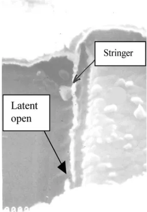
A special situation is given when we look at poly silicon stringers: they occur usually when topographical structures,
for example field oxide steps, perform slopes. In such cases, the slope angles are sometimes too high, so that poly silicon stringers remain along these slope borders (Fig.3). If two neighboured poly silicon lines pass such a slope, they may be electrically be shorted together by such a stringer (Fig. 3). The stringer thickness, however, is only very small compared to the regular poly silicon layer thickness. In the subsequent oxidation steps, not only the poly silicon lines are surface-oxidized but also the stringer
Fig. 1 At the touching points, the oxygen has no direct access to the polySi surface. At such points, the oxidation attack appears only from the side (here top and bottom of the touch point), resulting in a minor oxide thickness
Fig. 2 Examples for latent PolySi particle defects
Fig. 3 Poly silicon stringer a sublayer poly slope, sample directly taken after polySi etching process
However, in opposite to random poly silicon particles and residues, polySi stringers are a systematic failure: if the combination of poly silicon deposition, slope topography underneath and dry etching parameters perform the gen-eration of such stringers, they will occur nearly everywhere on the device. In the best case, the stringers are small enough to be completely reoxidized. In such case, they never will be discovered by any functional or reliability tests. If the stringers were too strong to be completely reoxidized, the problem would be a minor one, too: The device will fail in even the simplest functional test cate-gories and (hopefully) an effective failure analysis will quickly find them as the responsible root cause. The situ-ation, however, becomes a problem, if some few stringers are only slightly reoxidized. Since the etching behaviour on a wafer is never completely homogeneous, a variation in the evidence of stringer-related failures must be expected and in fact, this is (as many other failure mechanisms, too) often reflected in a wafer yield map, showing both good
and bad areas on the wafer. Considering poly silicon-stringer-related failures, the transient zone between both is most critical: Here, two effects can happen:
(a) Some few stringers are still not completely reoxidized and give very tiny shorts between neighboured poly silicon lines. In such case, electrical testing might fuse them and, thus ‘‘repair’’ the device, or, if the shorts are very high-ohmic, they may cause parametric deviations, leaving the chips at the border of specification.
(b) The stringers are partially reoxidized but perform still a conductive poly silicon core on a significant part of their length. In this case, corona discharge may start, hurting the remaining SiO2isolation and thus causing
soft damage.
Both mechanisms a and b may happen in the field application, too. From analytical point of view, it can be added that FIB cross sections of stringers show up clearly by passive potential contrast, whether they are isolated (=dark) or perform any remaining connection to the cir-cuitry (=bright), see Fig.6.
Special kinds of poly silicon stingers are the so-called fuse stringers. Many chips include poly fuses for the fuse trimming. By this, for example capacitors can be adjusted
Fig. 4 Reoxidized Stringer, still performing a connection between the top and bottom polySi line
Fig. 5 Inhomogeneous degree of reoxidation performs inhomoge-neous stringer thickness; small opens may cause latent defects
to resonance, customer-specific circuitry can be activated or deactivated or redundant circuitry can be switched.
The trimming of such fuses usually is performed by laser fuse-blow. If, however, the laser spot is misaligned or too weak in energy, it happens that the fuse is incompletely blown, leaving small stringer on one side of the poly-sili-con fuse. Thus, the fuse is still not open, giving probably malfunctions or parametric no expected behaviour to the circuitry (Fig.7).
A further (reliability) problem of poly silicon fuses are recombination effects. Since the laser brings the poly sili-con to a very high temperature, liquid poly-silisili-con drops locally may melt the thin passivation within the fuse frame
and short-circuit one of the fuse-line-ends to the metal frame. Also, the drops can completely recombine the fuse by bridging it with molten poly silicon, see Fig.8.
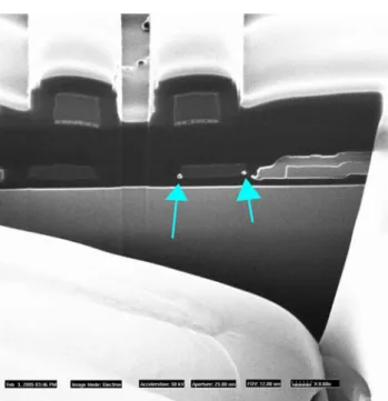
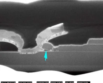
In techniques, which use two layers of poly silicon, residues of the second level of poly silicon can act very similar like those of the first poly Si level. The reason is the fact that only small oxide separates first from second level of poly silicon and, since at this level, no planarisation is usual, poly2 silicon residues could generate shorts between neighboured poly1 silicon lines as well as to neighboured contacts. Even shorts to contacts frequently occur as latent failures: while the etching attack of contact hole etching to the poly residue is an evident undesired connection, the short-circuit path to the neighboured poly silicon-1 line is still not connected due to slight reoxidation of both residue and poly-1 silicon (Figs.9,10,11). This effect is one of the most frequent reasons for field failures and reliability problems. Such effects can hardly been discovered in regular functional tests. Considering failure analysis aspects, such failures are usually indicated by emission microscopy. However, due to the limited resolution of emission microscope failure localisation, it frequently becomes difficult to distinguish between ESD failures, gate oxide breakdowns or poly-Si-related failures. Besides FIB cross sectional characterisation, a complete delayering performs footprints of the failure texture, which allow concluding correctly. Figure12 shows such delayering as an example for a polySi extension into a neighboured contact.
Fig. 8 Laser-trimmed polySi-fuses; the drops partially connect them to a metal ring, such either recombining them or giving connection to neighbour fuses
Fig. 6 FIB cross sectionn of a Si stringers: the bright points show that both stringers are connected to backward circuitry
Fig. 7 Sliced FIB cross section through a poly fuse stringer, beginning at the center (top left), ending at the full size of the fuse’s poly line (right bottom)
3 Testing and screening
When failures as described above, were found, in general one of the first questions is, how these devices could have passed the final functional test on wafer level. However, based on the explanations above, it becomes obvious that many failures of such kind are latent failures, where the breakdown through a small thickness of grown Silicon dioxide is necessary. In some cases, field failures have
shown even unbelievable structural damage, without showing time-zero functional failures. The example shown in Fig.13, however, shows proper oxidation lines along the structural damages. Knowing such risks, already many semiconductor -manufacturers and also some end users perform overvoltage stress testing (Bauch1998; Khalil and Wey2001). The intention of such testing, done by at least 25% above upper Vdd spec limit voltage, is, to provoke
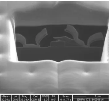
Fig. 11 PolySi extension, causing a hard short between polySi and contact
Fig. 9 Poly1-Si residue, causing a latent short between the contact and the neighboured first polySi. Note the small white lines at the border of the particle, indicating its reoxidation
Fig. 10 Poly2-Si resdue, performing the same mechanism like shown in Fig.9. Again, reoxidation can be seen by the small white lines
Fig. 12 By completely delayering all structure, the footprint allows to distinguish between ESD-related damage, gate oxide breakdowns and poly-extensions, like shown here
such kind of failures at an early stage of testing and, by this, to screen the production in a customer-useful manner. However, it must be carefully considered that many inte-grated circuits of today include internal voltage regulators, which prevent the device-internal circuitry from suffering the overvoltage. In such cases, an overvoltage test would not be useful to stress and screen such failures.
An additional or alternative method is, to integrate probable risk topographies for stringers in a slightly design-overcritical manner (e.g. reduced dimensions, superimpo-sition of critical topographies, etc.) into specific test chips (PCMs process control monitor devices). Such approach is very useful to find systematic problems like stringers, while it is not suitable for randomly distributed defects like particles and residues. If we compare the ratio of the very
small PCM area to the huge area of the wafer, the statistical probability to catch such failures on a PCM base is rather low. Only a catastrophic failure density could be detected with this. Nevertheless, the method could be considered for random process failures, too, if (a) related monitor area and numbers of PCM chips on the wafer is very high and (b) internal voltage regulators cannot be bypassed for over-voltage tests on regular devices.
4 Conclusion
Poly silicon related failures frequently appear as reliability problems due to their process-induced surface-oxidation. Besides actions against the process-related rood causes, the major issue is a successful monitoring, testing and screening in order to prevent end users from field-failures. The failure mechanisms include both systematic and ran-dom-process-defect related problems and some methods for their early screening have been pointed out.
Acknowledgments The author wants to express his thanks to his colleagues Giovanni Nicoletti (Empa), Florian Hauf and Uwe Thie-mann (Rood Technologies), Pascal Glauser and Philippe von Gunten (EM Microelectronic) for their excellent laboratory support in many internal and external customer analyses cases.
References
Bauch H (1998) Smart fabrication screening-HV-screening. In: Bosch presentation in Erfurt (Germany) at the workshop smart fabri-cation QM. Funded by German Ministry of Edufabri-cation and Research
Khalil MA, Wey CL (2001) High-voltage stress test paradigms of analog CMOS ICs for gate-oxide reliability enhancement. In: 19th IEEE proceedings on VLSI test symposium, VTS 2001. pp 333–338
Fig. 13 PolySi residue, causing a severe—but latent—structural failure. The case was functioal at final test but came to analysis as a field failure