Computational Study and Analysis of Structural Imperfections
in ID and 2D Photonic Crystals
by
Karlene Rosera Maskaly Bachelor of Science, Physics
Massachusetts Institute of Technology, 2000
Submitted to the Department of Materials Science and Engineering in Partial Fulfillment of the Requirements for the Degree of
Doctor of Philosophy in Materials Science and Engineering at the
MASSACHUSETTS INTITUTE OF TECHNOLOGY JUNE 2005
MASSACHUSETTS INSTTUTE
OF TECHNOLOGY
JUL 2 2 2005
LIBRARIES
© 2005 Massachusetts Institute of Technology. All Rights Reserved.
Signature ofAuthor .... ...
/ { rt ~ment of Werials Science and Engineering
-,/ /May 25, 2005
Certified
by ... .
.; ...
...
W. Craig Carter Lord Foundation Professor of Materials Science and Engineering
i .~_~4 Thesis supervisor
Certified by ... ...
Yoel Fink Thomas B. King Assistant Professor of Materials Science Thesis supervisor Accepted by ...
C'~- "Gerbrand .. Ceder R.P. Simmons Professor of Materials Science and Engineering Chair, Departmental Committee on Graduate Students
Computational Study and Analysis of Structural Imperfections
in D and 2D Photonic Crystals
By
Karlene Rosera Maskaly
Submitted to the Department of Materials Science and Engineering on May 25th, 2005 in partial fulfillment of the
requirements for the degree of Doctor of Philosophy in Materials Science
Abstract
Dielectric reflectors that are periodic in one or two dimensions, also known as 1D and 2D photonic crystals, have been widely studied for many potential applications due to the presence of wavelength-tunable photonic bandgaps. However, the unique optical
behavior of photonic crystals is based on theoretical models of perfect analogues. Little is known about the practical effects of dielectric imperfections on their technologically useful optical properties. In order to address this issue, a finite-difference time-domain (FDTD) code is employed to study the effect of three specific dielectric imperfections in
1D and 2D photonic crystals. The first imperfection investigated is dielectric interfacial roughness in quarter-wave tuned ID photonic crystals at normal incidence. This study reveals that the reflectivity of some roughened photonic crystal configurations can change up to 50% at the center of the bandgap for RMS roughness values around 20% of the characteristic periodicity of the crystal. However, this reflectivity change can be mitigated by increasing the index contrast and/or the number of bilayers in the crystal. In order to explain these results, the homogenization approximation, which is usually
applied to single rough surfaces, is applied to the quarter-wave stacks. The results of the homogenization approximation match the FDTD results extremely well, suggesting that the main role of the roughness features is to grade the refractive index profile of the interfaces in the photonic crystal rather than diffusely scatter the incoming light. This result also implies that the amount of incoherent reflection from the roughened quarter-wave stacks is extremely small. This is confirmed through direct extraction of the amount of incoherent power from the FDTD calculations. Further FDTD studies are done on the entire normal incidence bandgap of roughened ID photonic crystals. These results reveal a narrowing and red-shifting of the normal incidence bandgap with
increasing RMS roughness. Again, the homogenization approximation is able to predict these results. The problem of surface scratches on ID photonic crystals is also addressed. Although the reflectivity decreases are lower in this study, up to a 15% change in
reflectivity is observed in certain scratched photonic crystal structures. However, this reflectivity change can be significantly decreased by adding a low index protective coating to the surface of the photonic crystal. Again, application of homogenization theory to these structures confirms its predictive power for this type of imperfection as well. Additionally, the problem of acircular pores in 2D photonic crystals is investigated,
showing that almost a 50% change in reflectivity can occur for some structures. Furthermore, this study reveals trends that are consistent with the D simulations: parameter changes that increase the absolute reflectivity of the photonic crystal will also increase its tolerance to structural imperfections. Finally, experimental reflectance spectra from roughened D photonic crystals are compared to the results predicted computationally in this thesis. Both the computed and experimental spectra correlate favorably, validating the findings presented herein.
Keywords: Photonic Crystals, Bragg Mirror, Roughness, Imperfections, FDTD
Thesis Supervisor: W. Craig Carter
Title: Lord Foundation Professor of Materials Science and Engineering
Thesis Supervisor: Yoel Fink
Acknowledgements
The Lord is my strength and my shield;
My heart trusts in Him, and I am helped;
Therefore my heart exults,
And with my song I shall thank Him. (Psalm 28:7 NASB)
There are so many people that have helped me through these past several years. But first and foremost, I would like to acknowledge the one who has played the most critical role in bringing me to this point: my Lord and Savior Jesus Christ. It is through Him that I had the strength, patience, courage, wisdom, and faith to persevere through the most difficult times during graduate school. Indeed, when I first began my studies at MIT, I did not know God. I relied on myself for earthly gains and was often disappointed when I fell short. For some reason, I began attending bible studies during my second year of graduate school. Looking back, I cannot remember any logical reason why I began doing this. But it was during these bible study sessions that I grew in knowledge, and therefore love, of God. And this is by far the most valuable thing I have gained from my time in graduate school. In the words of Paul:
...I count all things to be loss in view of the surpassing value of knowing Christ Jesus my Lord ... and count them but rubbish so that I may gain Christ, and may be found in Him,
not having a righteousness of my own derivedfrom the Law, but that which is through .faith in Christ ... that I may know Him and the power of His resurrection ... in order that
I may attain to the resurrection from the dead. (Philippians 2:10-11 NASB)
In addition to the promise of eternal salvation, love and trust in God also brings with it a promise for our life here on earth:
And we know that God causes all things to work together for good to those who love God, to those who are called according to His purpose. (Romans 8:28 NASB)
It was the knowledge of this truth that carried me through one of the most difficult times in my life.
But I would be amiss if I did not also acknowledge the people that God put into my life to help me through these times. First, I would like to thank my husband, Garry. Some people may think that seeing your husband almost every hour of the day both at work and at home would become unbearable. But I truly count that as one of the most special blessings that God gave me during graduate school. I would often trot down to his floor when I was troubled, or bored, or just wanted to get a snack - and being near him would always bring joy to my heart and could easily turn a bad day into a good one. Not only was Garry always there to emotionally help me through difficult times, he also had the knowledge to advise me through those times as well. This also made him one of the most intellectually influential people in my life during my graduate studies.
I would also like to thank the members of the Thursday night GCF bible study and Praisedance, who supported me through their endless prayers and words of
encouragement. Indeed, their efforts helped me to focus on that which is most important. I would especially like to thank Shandon Hart, who first introduced me to the bible study and helped both me and Garry grow immensely in our faith. I really want to thank him
for the love, guidance, and fellowship he gave to us, which made graduate school a truly joyful time in my life. He taught us what it means to be a true follower of Christ, and I
have yet to meet another person as kind, loving, compassionate, thoughtful, and wise as him and his wife Colleen. Knowing them has been a real blessing.
I would also like to thank my advisor, Prof. Craig Carter. From the beginning, he has been an extraordinary advisor. Two and a half years ago, I came to him with a research idea but, of course, no funding. And even though the research was not in his area of interest, he used money that he could have done anything else with to fund my idea. This was a genuinely magnanimous gesture that I will never forget. Furthermore, he gave me freedom in my research for which I am very grateful. And finally, he and Marty have been extremely kind to me, allowing me to intrude on their home while I was preparing for my preliminary defense. Having an advisor like Craig is extremely rare, and I want to thank him for taking me in as a student even when there wasn't really any room in his group.
I also want to thank all the members of Prof. Carter's group. They all put up with me using basically any CPU in the group I could get my hands on to do my simulations. Rick and Colin were especially patient with me when I had computer problems. Rick spent so much time setting up the machines and trying to install random 3D graphics packages for me that never ended up working. Colin toiled away at ensuring that the machines were secure and, of course, rebooting my computer at MIT when it crashed while I was working at LANL. But I can't forget Ming's late hours that comforted me when I wasn't the only one working late, and also saved me when I needed a computer to be rebooted on Christmas Eve. And of course, there's Ellen. Her unique personality really helped me to laugh and have a life outside of research (e.g. the walk for hunger). She has been a really great friend and I already miss her.
Cody and Kristy Friesen have also been very good friends to Garry and I throughout graduate school. They helped us relax by joining us on trips to Canada and North Carolina, as well as numerous skiing trips. And we had countless hours of fun just going out to dinner or movies or candlepin bowling. Additionally, Cody helped me a lot with some of my initial research, for which I am also grateful.
Even though Prof. Yet-Ming Chiang was not one of my advisors, I want to
acknowledge the kindness he and his group showed me during graduate school. Initially, my research involved experiments. However, because Prof. Carter only does
computational work, I had no labs in which to do the experiments. So Prof. Chiang allowed me to crowd into his space and use his equipment (at no cost). In addition, the members of his group were very nice to me and treated me like I was also a member of the group. I especially want to thank Steven who was a very good friend to both Garry and me.
I also want to acknowledge the help that Prof. Yoel Fink and his group gave me. Yoel helped me to think more critically about some of the most difficult problems in my thesis. In addition, the members of his group, especially Ofer and Shandon, were kind enough to set aside some of their time to help me with various aspects of my research.
While I was working at LANL, Rick Averitt and James Maxwell served as mentors to me. It is truly amazing how God looked after me for this portion of my research. For here too, I was blessed with two remarkable mentors who spent money to fund me on a project that was outside their field of interest and gave me the freedom to
do the research I needed to finish my thesis. This allowed Garry and me to stay together during his internship and subsequent postdoc appointment at LANL, while still making progress on my thesis.
At Los Alamos, I was also blessed with many friends that prayed for me and helped me through the most difficult part of my thesis - the writing and defense. I especially want to thank Doug and Marci, Kate and Neil, and Jennifer and Neil for their support and prayers.
Lastly, I would like to thank both my parents and Garry's parents for the support they have given me. In their own quiet way, my parents stood by me through both the triumphs and the struggles in my life. Whatever happened, I knew they would always be proud of me. They never pushed me to be something I didn't want to be, and they never expected more from me than what I could do while still being happy. As for Garry's parents, from the first time I met them, they have treated me like I was their own
daughter. The love and support they have given me is remarkable, and I am so thankful that they are part of my life.
The research in this thesis was supported by the MIT-Singapore Alliance, the Los
Alamos National Laboratory Directed Research and Development Program, and the U.S. Army through the Institute for Soldier Nanotechnologies under contract DAAD-19-02-D-0002 with the U.S. Army Research Office. The content does not necessarily reflect the position of U.S. government, and no official endorsement should be inferred.
Scripture quotations taken from the New American Standard Bible®, Copyright C 1960, 1962, 1963, 1968, 1971, 1972, 1973,
1975, 1977, 1995 by The Lockman Foundation Used by permission. (www.Lockman.org)
Table of Contents
List of Figures ... 11
Glossary of Symbols ... 19
Chapter 1: Introduction ... 23
Chapter 2: An Introduction to Electromagnetism and Photonic Crystals ... 29
2.1 The Maxwell Equations and the Helmholtz Wave Equation ... 30
2.2 The Behavior of Light at Boundaries ... 34
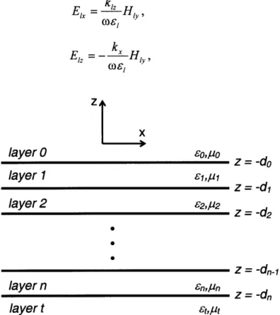
2.3 Systems with Multiple Interfaces ... 42
2.4 Photonic Crystals ... 46
2.5 Mie Scattering Theory ... 51
Chapter 3: Methods for Simulating Electromagnetic Responses ... 57
3.1 1D Transfer Matrix Method ... 58
3.2 Frequency Domain Method ... ... 60
3.3 Finite Difference Time Domain (FDTD) Method ... 61
Chapter 4: Interfacial Roughness in D Photonic Crystals: An FDTD Study ... 69
4.1 Interfacial Roughness Parameters ... 72
4.2 Generation of the Roughened Structures ... 73
4.3 Simulation and Analysis Method ... 76
4.4 TE Polarization Reflectivity Results ... 80
4.5 TM Polarization Reflectivity Results ... 86
4.6 Conclusions ... 88
Chapter 5: A Scattering Model of Interfacial Roughness ... 91
5.1 Scattering Model ... 93
5.2 Implementation of the Model ... 97
5.3 Results of the Model ... 100
5.4 Conclusions ... 104
Chapter 6: Homogenization and Kirchhoff Approximations for Interfacial Roughness 107 6.1 The Homogenization Approximation ... ... 108
6.2 The Kirchhoff Approximation ... 109
6.3 Implementation of the Homogenization Approximation ... 111
6.4 Implementation of the Kirchhoff Approximation ... 113
6.5 Results of the Applied Approximations ... 114
6.6 Conclusions ... 120
Chapter 7: Calculation of the Scattered Power from Interfacial Roughness ... 123
7.1 General Form of the Reflected Wave ... ... 124
7.2 Calculation of the Scattered Power ... 126
7.3 Results for the Simulated Structures ... 130
7.4 Conclusions ... 136
Chapter 8: Effect of Interfacial Roughness on the Normal Incidence Band Gap ... 139
8.1 FDTD Reflectivity Results ... 140
8.2 Homogenization Approximation Reflectivity Results ... 144
Chapter 9: Surface Scratches on D Photonic Crystals ... 153
9.1 Surface Scratch Parameter ... 154
9.2 Generation of the Scratched Structures ... 155
9.3 FDTD Reflectivity Results ... 157
9.4 Homogenization Approximation Reflectivity Results ... 163
9.5 Conclusions ... 163
Chapter 10: Acircular Pores in 2D Photonic Crystals ... 169
10.1 Determination of Simulation Conditions ... ... 172
10.2 Porous Acircularity Parameter ... 173
10.3 Generation of the Acircular Structures ... 174
10.4 Simulation Equilibration ... ... 177
10.5 Porous Alumina Reflectivity Results ... 178
10.6 Porous Silicon Reflectivity Results ... 180
10.7 Conclusions ... 184
Chapter 11: Experimental Corroboration ... 187
11.1 Calculated Reflectance Spectra for Two Rough Structures ... 189
11.2 Proposed Experiments ... 193
Chapter 12: Conclusions and Future Work ... 199
Appendix A: Code for the Simulation of Actual Roughened Structures ... 205
List of Figures
Figure 2.1 Reflection and transmission at a plane boundary from a TE polarized incident plane w ave ... 35 Figure 2.2 TE and TM reflection off a plane boundary with Ai=t=l .0, i=1.0, and ,t=4.0.
The Brewster angle, where the TM reflectivity goes to zero, is clear ... 41
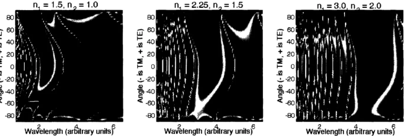
Figure 2.3 A structure consisting of n interfaces, with the position of each interface given by z = -d/ ... 42 Figure 2.4 Possible photonic crystal architectures. The dielectric periodicity can occur in one dimension, two dimensions, or three dimensions [Joannopoulos (1995), reprinted with permission from Princeton University Press] ... 47 Figure 2.5 Plot of the reflectivity versus wavelength and incident angle for three
different photonic crystal structures. The red region in each plot indicates a high reflectivity, while the blue region corresponds to a low reflectivity. All three systems have 4 bilayers with nl=2.25 and n2=1.5. However, the volume fraction of the
constituent materials changes, as indicated by the t and t2 values. The center plot
corresponds to a quarter-wave stack configuration. ... 48 Figure 2.6 Plot of the reflectivity versus wavelength and incident angle for three quarter-wave stack structures that all have 4 bilayers and nl/n2= 1.5. As the average refractive index of the structure increases, the width of the bandgap also increases ... 49
Figure 2.7 Plot of the reflectivity versus wavelength and incident angle for three quarter-wave stacks that all have 4 bilayers and average refractive indices of 1.875. As the index contrast of the photonic crystal increases, the absolute reflectivity in the bandgap also increases ... 50 Figure 2.8 Plot of the reflectivity versus wavelength and incident angle for three quarter-wave stacks with various bilayers. All structures have n1=2.25 and n2=1.5. As the
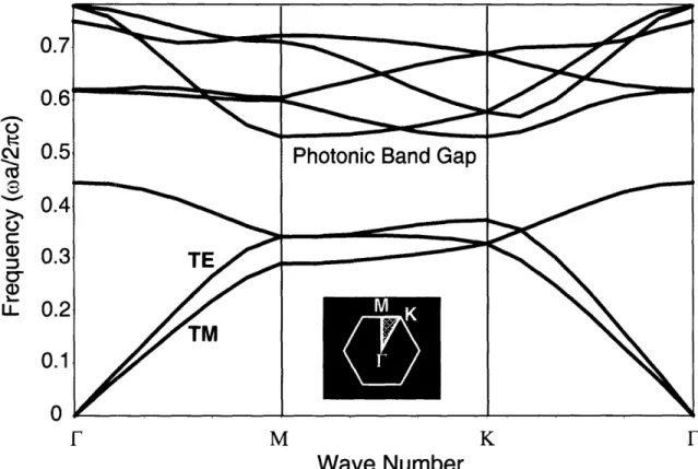
number of bilayers increases, the absolute reflectivity in the bandgap also increases ... 50 Figure 2.9 Band diagram for a 2D hexagonal lattice (shown in the inset) where the pores/rods have a refractive index of 1.0 and the matrix has a refractive index of 3.5. Also shown is the Brillouin zone with the irreducible section shaded in yellow. The photonic bandgap, where no eigenmodes exist for any wave vector, is shown in yellow.51 Figure 2.10 Angle-dependent scattering intensity as a function of scatterer radius from perpendicularly polarized incident light at wavelength o0. As the radius (indicated on top
of each plot) increases, the magnitude of the scattered intensity also increases. The index contrast between the scatterer and the ambient was 1.5 in all cases ... 53 Figure 2.11 Angle-dependent scattering intensity as a function of index contrast from perpendicularly polarized incident light at wavelength 2o. As the index contrast
increases, the amount of scattered intensity also increases at every angle. The radius of the scatterer here is 0.102o. ... 54 Figure 3.1 Schematic of the simulation domain illustrating the unidirectional source that allows separation of the total field and the reflected field ... 64 Figure 4.1 One example of a "real world" structure with a large amount of interfacial roughness. This particular structure is a liquid crystal multilayer fabricated by K. Hsiao, et al. [Hsiao (2004), reprinted with permission]. The micrograph on the left is the actual structure, while the schematic on the right is the idealized structure on which the
theoretical optical response of the device is based. ... 70 Figure 4.2 A micrograph of a porous silicon multilayer structure fabricated by Agarwal, et al. (reprinted with permission from V. Agarwal and J. A. del Rio, Applied Physics
Letters, 82, 1512 (2003), copyright 2003, American Institute of Physics). Although this
structure does not deviate from its ideal as much as the structure in Fig. 4.1, some amount of interfacial roughness is still evident. ... 71
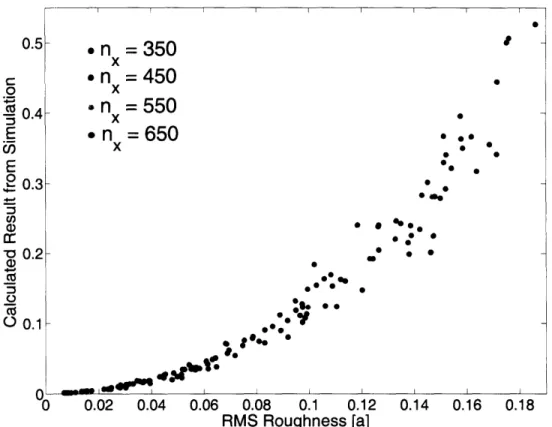
Figure 4.3 Schematic of the rough interfaces in the simulated structures illustrating the two parameters that were used to characterize each roughened structure: RMS roughness and RMS wavelength. Also shown is the characteristic periodicity (a) of the photonic crystal ... 72 Figure 4.4 Close up of a roughened interface illustrating the process used to create the roughness features... 75 Figure 4.5 Simulation results showing that the size of the domain between periodic walls was sufficiently large. The distance between periodic walls is given by the parameter n,x. An nx value of 450 was used for all the FDTD simulations presented in this thesis ... 77 Figure 4.6 The equilibration of three simulated bilayer systems. The pink region
corresponds to the time steps over which the time average was taken in Eq. 4.9 ... 78 Figure 4.7 The calculated percent change in the TE-polarized normal incidence
reflectivity for roughened 4-bilayer quarter-wave stacks with nl=2.25 and n2=1.5. Also
shown are four example structures for four particular simulations ... 81 Figure 4.8 The calculated percent change in reflectivity for several 4-bilayer
quarter-wave stack configurations. Empirical fits to the data, with index contrast and number of bilayers as the only parameters, are also shown. ... 82
Figure 4.9 The calculated percent change in reflectivity for several nl=2.25, n2=1.5 quarter-wave stack configurations with varying bilayer numbers. Again, empirical fits to the data, with index contrast and number of bilayers as the only parameters, are also show n .. ... 84 Figure 4.10 The calculated percent change in the TM-polarized normal incidence
reflectivity for roughened 4-bilayer quarter-wave stacks with nl=2.25 and n2=1.5 ... 87
Figure 4.1 1 Comparison of the TE and TM polarization reflectivity results ... 88 Figure 5.1 Schematic illustrating the idea of mimicking the change in reflection and transmission due to the roughness features by replacing the rough surface with a smooth surface and correspondingly modifying its refractive index ... 93
Figure 5.2 Transmissivity vs. the transmitting medium's refractive index (nt) for an incident medium with refractive index ni=1.5. Notice that for a given transmissivity (t) there are two possibilities for nt, one larger than n and one smaller ... 95 Figure 5.3 Illustration of the four distinct interfaces in the simulated quarter-wave stacks. Each interface results in a different amount of scattering ... 97 Figure 5.4 Schematic illustrating that the incident wavelength for each interface depends on the refractive index of the preceding layer, while the scatterer size remains the same.
...
99
Figure 5.5 The index modification process applied to a 4-bilayer structure with nl=2.25, n2,=1.5, and RM = 0. la ... 101
Figure 5.6 Index modification results for the same 4-bilayer systems presented in chapter 4. The scatterer sizes reported on the plot have been scaled to the equivalent RMS
roughness value. The trends predicted with this model agree with the FDTD results.. 102 Figure 5.7 Index modification results for the same nl=2.25, n2=1.5 bilayer systems presented in chapter 4. The scatterer sizes above have been scaled to their equivalent
R,MS value. Again, the trends are consistent with those seen from the FDTD results... 103 Figure 5.8 Comparison of the results from the FDTD calculations and the index
modification model for the 4-bilayer nl=2.25, n2=1.5 system. Although the index
modification model correctly predicts the trends seen with the FDTD calculations, it fails to reproduce the actual magnitude and curve shape of the FDTD data ... 104
Figure 6.1 Schematic depicting the homogenization approximation for a single rough interface. The dielectric constant in the region of the rough interface is average to produce a smoothed dielectric constant function. The smooth dielectric constant is then approximated with a series of layers ... 109
Figure 6.2 Schematic depicting the Kirchhoff approximation for a single rough interface. The reflectivity of the roughened surface is estimated by averaging the reflection
coefficients from several smooth surfaces with varying heights. The height distribution of the smooth structures is equal to the height distribution of the rough interface ... 110 Figure 6.3 Application of the homogenization approximation to the roughened quarter-wave stacks. The dielectric constant is averaged across each row of the input structure.
The smooth profile is then converted into a series of layers ... 111
Figure 6.4 The averaged refractive index profiles for four RRMs values in the 4-bilayer,
nl=2.25, n2=1.5 system. For the RRMS values of 0.1453a and 0.1759a, the index of
refraction in the approximated structure never reaches the extreme values of 2.25 and 1.5. ... 112
Figure 6.5 Application of the Kirchhoff approximation to the roughened quarter-wave stacks. The structure is broken up into many structures by taking each column of the rough structure as a separate 1D structure. The reflection coefficients for each structure are calculated and averaged to give the estimated reflectivity of the roughened structure.
... 113
Figure 6.6 Comparison of the FDTD results with the results of both the homogenization and Kirchhoff approximations for the same 4-bilayer systems presented in chapter 4. The Kirchhoff approximation does a poor job at reproducing the data, but the homogenization approximation matches the FDTD results very well ... 115 Figure 6.7 Explanation for why the Kirchhoff approximation under-estimates in some
cases and over-estimates in others. The pink region is the quarter-wave tuned wavelength. The dashed line is the FDTD result and the dotted line is the Kirchhoff result ... 117 Figure 6.8 Comparison of the FDTD results with the results of both the homogenization and Kirchhoff approximations for the n1=2.25, n2=1.5 systems presented in chapter 4. Again, the Kirchhoff approximation does not predict the FDTD results, while the
homogenization approximation matches them very well ... 119 Figure 7.1 The simulated reflected wave for one of the roughened structure. As shown, the photonic crystal is positioned behind the wave. Thus, the direction of propagation is out of the page. The periodic boundaries of the domain are located along the yz planes.
... 127
Figure 7.2 The residual of the fit to the reflected wave. The orientation of the photonic crystal is the same as that in Fig. 7.1. The second order Floquet mode (evanescent) and the incoherent field are apparent ... 128
Figure 7.3 Incoherent power from the 4-bilayer nl=2.25, n2=1.5 system. Note that the
largest amount of incoherent power is only about 10- 3for an incident wave power of 1.0.
... 130
Figure 7.4 The power in the propagating Floquet mode for the 4-bilayer, nl=2.25, n2=1.5
system. Again, note that the maximum power is only 10-2 for an incident wave power of 1 ... ... 131
Figure 7.5 The incoherent power from two 4-bilayer systems presented in chapter 4:
nj=2.25, n2=1.5, and nl=3.0, n2=1.5. The higher index contrast system shows slightly
more incoherent power, but the magnitude is still extremely small (< 10-3 ) ... 132
Figure 7.6 The power in the propagating Floquet mode from the same two 4-bilayer systems shown in Fig. 7.6. Again, the magnitude of the power in both systems is
extremely small (< 10-2) ... 133
Figure 7.7 Mie theory prediction of the amount of scattered power from the high-to-low index interfaces in the nl=2.25, n2=1.5 and nl=3.0, n2=1.5 structures. Notice that both the
curve shape and the trend predicted here are consistent with the incoherent power
calculation from the FDTD data of the same systems ... 134
Figure 7.8 The percentage of reflected power that is carried by scattered light (incoherent plus Floquet mode) for the nl=2.25, n2=1.5 and nl=3.0, n2=1.5 systems. In the worst
case, only 4.5% of the reflected power is carried by scattered light ... 135
Figure 8.1 The simulated normal incidence reflectance spectra corresponding to several 4-bilayer systems. In all systems, a narrowing and red-shifting of the normal incidence bandgap is apparent ... 142 Figure 8.2 The percent change in reflectivity (Ar) across the entire normal incidence bandgap for several 4-bilayer systems. The shading indicates the region where the reflectivity of the bandgap is within 10% of its maximum value. Again, the red-shift is apparent in all systems ... 143
Figure 8.3 The simulated normal incidence reflectance spectra corresponding to several bilayer systems with n1=2.25 and n2=1.5. Again, a narrowing and red-shifting of the
bandgap is evident in all systems ... 145
Figure 8.4 The percent change in reflectivity (Ar) across the entire normal incidence bandgap for several bilayer systems with nl=2.25 and n2=1.5 ... 146 Figure 8.5 The results of the homogenization approximation applied to the 4-bilayer structures presented in Fig. 8.1. Comparison of the two figures shows that the
Figure 8.6 The results of the homogenization approximation applied to the 4-bilayer structures presented in Fig. 8.2 ... 149 Figure 8.7 The results of the homogenization approximation applied to the bilayer
systems shown in Fig. 8.3. Again, comparison of the two figures shows that the
homogenization approximation is in good agreement with the FDTD results ... 150 Figure 8.8 The results of the homogenization approximation applied to the bilayer
structures presented in Fig. 8.4 ... 151
Figure 9.1 The percent change in reflectivity (Ar) for several 4-bilayer quarter-wave stacks with different constituent refractive index values. In addition to structures without protective coatings, structures with coatings were also tested in all of the systems. The coatings had refractive index values of 1.5, 2.0, and 2.5 ... 158 Figure 9.2 The normal incidence bandgap for a unscratched 4-bilayer nl=2.25, n2=1.5
structure with (top) and without (bottom) a protective coating. The coating used for the bottom structure had a refractive index of 1.5 (beneficial coating) ... 160 Figure 9.3 The effect of surface scratches on the normal incidence bandgap for two 4-bilayer n1=2.25, n2=1.5 structures. The top structure has no protective coating, while the
bottom structure has an n¢=1.5 coating (beneficial coating) ... 161
Figure 9.4 Percent change in reflectivity (Ar) for two 4-bilayer structures with nl=2.25 and n2=1.5. The top structure has no protective coating, while the bottom structure has an nc=1.5 coating (beneficial coating) ... 162
Figure 9.5 The results of the homogenization approximation for the 4-bilayer nl=2.25, n2=1.5 structures presented in Fig. 9.1. As with the other studies, the homogenization
approximation correctly predicts the FDTD results for the scratched structures ... 164 Figure 9.6 The homogenization approximation results for the 4-bilayer, nl=2.25, n2=1.5
systems across the entire normal incidence bandgap. The benefit of an nc/nl < 1.0 coating is correctly predicted with the approximation ... 165 Figure 10.1 Two micrographs of porous alumina. The structure in the left micrograph was produced under controlled anodization conditions, while the structure on the right was fabricated with poor control over the anodization process ... 170 Figure 10.2 A micrograph of porous indium phosphide [Carstensen (2005),
Christophersen (2005), reprinted with permission]. Although this structure does not deviate from its ideal as much as the porous alumina in Fig. 10.1, some amount of pore acircularity is still evident ... 171 Figure 10.3 Schematic of the hexagonal lattice used in the simulations. The Brillouin zone, with the irreducible section shaded, is also shown superimposed on the lattice. The
direction of the incident wave vector is coincident with the M-point of the irreducible Brillouin zone ... 172 Figure 10.4 The TE bandgap in porous alumina, and the TE and TM bandgaps in porous silicon are shown as a function of the pore radius (r) normalized to the center-to-center distance between pores (a). These maps were calculated for the perfect structures using the MPB frequency domain code [Johnson (2001), Johnson (2005)] ... 173
Figure 10.5 Schematic illustrating the range of curvature radii that characterize an acircular pore. The RMS acircularity (ARMS) is defined as the RMS radius of curvature deviation from the mean radius of the pore ro ... 174 Figure 10.6 Schematic of the simulated hexagonal lattice illustrating the relevant
param eters ... 175 Figure 10.7 Results of the equilibration run for both the 8 row and 12 row structures. The initial large transient behavior is gone by about the 2 0,0 0 0th step in both cases. The shaded region indicated the time steps over which the time-averaging was done in the reflectivity calculation ... 179 Figure 10.8 The percent change in the TE polarized reflectivity (Ar) for 8 and 12 row structures of porous alumina. Also shown are two example structures corresponding to the most extreme structural deviations tested in this study ... 180 Figure 10.9 The percent change in the TM polarized reflectivity (Ar) for 8 and 12 row structures of porous silicon. Again, two example structures are shown that corresponding to the most extreme structural deviations tested in this study. The architectural deviations in these structures are much more severe than those in the porous alumina study ... 181
Figure 10.10 The percent change in the TE polarized reflectivity (Ar) for 8 and 12 row structures of porous silicon. Two example structures with much lower ARMS values are shown for comparison with those in Figs. 10.8 and 10.9 ... 182
Figure 10.11 The percent change in the TM polarized reflectivity from the porous silicon system for A MS values less than 0.04r ... 183
Figure 10.12 The percent change in the TE polarized reflectivity from the porous silicon system for A Ms values less than 0.04r ... 184
Figure 11.1 One of the "real-world" roughened structures analyzed with the
homogenization approximation [Hsiao (2005), reprinted with permission] ... 189 Figure 11.2 Experimental reflectance spectrum for the structure shown in Fig. 11.1
Figure 11.3 Results of the homogenization approximation applied to the structure shown in Fig. 11.1 ... 191
Figure 11.4 The second roughened structure analyzed with the homogenization
approximation [Hsiao (2005), reprinted with permission]. Although it is not apparent to the eye, there are three periodicities built into the structure. ... 192 Figure 11.5 Experimental reflectance spectrum for the structure shown in Fig. 11.4 [Hsiao (2005), reprinted with permission]. Notice the three distinct reflectivity peaks. 193 Figure 11.6 Results of the homogenization approximation applied to the structure shown in Fig. 11.4. Again, note the three distinct reflectivity peaks ... 194
Glossary of Symbols
Al Field amplitude of the positive z propagating waves in the I layer A RMS RMS pore acircularity
B Magnetic flux density vector
B1 Field amplitude of the negative z propagating waves in the I layer
Cang, Angular cross section of scattered light polarized parallel to the scattering plane D Electric displacement vector
D:"(id) z-component of electric displacement field at the position i for the time step n
E Electric field vector
E i Incident electric field component that is parallel to the scattering plane
E, IS Scattered electric field component that is parallel to the scattering plane
E,n Coherent electric field magnitude
El st Floquet mode electric field magnitude En6, mth Floquet mode electric field magnitude Ei Incident electric field vector
Eit Transverse incident electric field magnitude
Eio Incident electric field magnitude vector E,o Total magnitude of incident electric field
E,~x x-component magnitude of incident electric field
E,y y-component magnitude of incident electric field
Ei= z-component magnitude of incident electric field
E,x x-component magnitude of the electric field in the layer
E,y y-component magnitude of the electric field in the layer
E,z z-com.ponent magnitude of the electric field in the I layer Er Reflected electric field vector
E,. Reflected electric field
E,/t Transverse reflected electric field magnitude
E,0 Reflected electric field magnitude vector
E,! Transmitted electric field vector
Elt Transverse transmitted electric field magnitude E,0o Transmitted electric field magnitude vector
E,x x-component magnitude of transmitted electric field
Ey y-component magnitude of transmitted electric field
Ez z-component magnitude of transmitted electric field
E), y-component magnitude of total electric field above boundary
E:.(ij) z-component of electric field at the position i for the time step n
H Magnetic field strength vector
H,ix x-component magnitude of incident magnetic field
Hy y-component magnitude of incident magnetic field
Hi z-component magnitude of incident magnetic field
HX x-component magnitude of the magnetic field in the layer
Hi z-component magnitude of the magnetic field in the layer
Hx x-component magnitude of total magnetic field above boundary
Hn(ij) x-component of magnetic field at the position ij for the time step n
Hyn(ij)y-component of magnetic field at the position ij for the time step n
H- z-component magnitude of total magnetic field above boundary
Ifs Forward-scattered intensity J Electric current density
L Length along boundary
Pfs Forward-scattered power from a volume of scatterers
R Fresnel reflection coefficient for a boundary
RI+)l Fresnel reflection coefficient between the layer and the 1+1 layer (see Eq. 2.82)
RRs RMS roughness
S Poynting power vector
S1 ,2,3,4 Amplitude scattering matrix components
T Transmission coefficient for a boundary To Time at which the time-average is begun
Ta Time over which the time-average is taken
V(7+l)l Transfer matrix between the layer and the 1+1 layer
WRMS RMS roughness wavelength
a Bilayer thickness in 1D photonic crystals, Pore center-to-center distance in 2D photonic crystals
an Scattering coefficient involving Riccati-Bessel function
bn Scattering coefficient involving Riccati-Bessel function
c Speed of light ( = 3 x 10⁸ meters/second in vacuum)
di Position of the interface
ill Scattered intensity per unit incident intensity for light polarized parallel to the scattering plane
k Wave vector
k Wave vector magnitude ki Incident field wave vector
ki Total magnitude of incident field wave vector
kix x-component magnitude of incident field wave vector
kiy y-component magnitude of incident field wave vector
kiz z-component magnitude of incident field wave vector
kz z-component magnitude of the field in the I layer kr Reflected field wave vector
kr Total magnitude of reflected field wave vector
krx x-component magnitude of reflected field wave vector kry y-component magnitude of reflected field wave vector kt Transmitted field wave vector
kt Total magnitude of transmitted field wave vector
ktx x-component magnitude of transmitted field wave vector
ky y-component magnitude of transmitted field wave vector
kt z-component magnitude of transmitted field wave vector
keg x-component magnitude of mth Floquet mode wave vector
kyc y-component magnitude of coherent electric field wave vector
kfi y-component magnitude of 1st Floquet mode wave vector
k&g y-component magnitude of mth Floquet mode wave vector
n Integer
nl High refractive index in 1D photonic crystals
n2 Low :refractive index in 1D photonic crystals
nc Refractive index of protective coating
ncirc Number of nodes along the circumference of the pores
ni Refractive index of incident medium (above boundary)
n,odes Number of nodes on rough interface
npv Number of peak or valley pairs on rough interface
ns Time step number
nT Number of time steps over which time-averaging is done
n,, Refractive index of transmitting medium (below boundary)
num_bilayers Number of bilayers in 1D photonic crystals
num_columns Number of columns of pores in 2D photonic crystals
numrows Number of rows of pores in 2D photonic crystals
n,, Number of nodes perpendicular to layers in 1D photonic crystals or parallel to columns in 2D photonic crystals
n, Number of nodes parallel to layers in 1D photonic crystals or parallel to rows in 2D photonic crystals
pit Ratio of incident to transmitted wave vector magnitudes (see Eqs. 2.51 and 2.61)
P(+)l Ratio of the wave vectors in the 1+l layer and the layer (see Eqs. 2.78 and 2.79) r Radial spatial distance coordinate vector
r Reflectivity
rc0 Mean pore radius of curvature of 2D photonic crystal
ri Radius of curvature of acircular pore
rrough Reflectivity of 1D photonic crystal with rough interfaces
rsmooth Reflectivity of 1D photonic crystal with smooth interfaces (perfect structure)
t Transmissivity
tl Thickness of high refractive index layer in quarter-wave tuned 1D photonic crystal
t2 Thickness of low refractive index layer in quarter-wave tuned 1D photonic crystal
tri,A Resonant transmission thickness for a wavelength of A
x x spatial distance coordinate
XPV) x-coordinate of the first peak or valley in the pair ,'V(2 x-coordinate of the second peak or valley in the pair
y y spatial distance coordinate
.yo y-coordinate of the mean interface position
yi y-coordinate of the actual (rough) interface position z z spatial distance coordinate
Ar Percent change in reflectivity of imperfect structure from perfect structure At Time step magnitude
Ay Grid cell width in y direction
E Dielectric constant
Eo Permittivity of free space (= 8.85 x 10- 12 farad/meter)
1i Dielectric constant of incident medium (above boundary) ct Dielectric constant of the layer
t Dielectric constant of transmitting medium (below boundary)
0i Angle between the incident wave vector and the normal of the boundary
0r Angle between the reflected wave vector and the normal of the boundary
Ot Angle between the transmitted wave vector and the normal of the boundary
A Wavelength
2o Nodal wavelength corresponding to the quarter-wave tuned wavelength
Ac Spatial wavelength corresponding to the quarter-wave tuned wavelength Al Spatial wavelength of the blue end of the bandgap
/10 Nodal wavelength of the blue end of the bandgap
Ah Spatial wavelength of the red end of the bandgap
AhO Nodal wavelength of the red end of the bandgap P Permeability
uo Permeability of free space ( = 4r x 10- 7henry/meter)
pA Permeability of incident medium (above boundary) ul Permeability of the layer
ut Permeability of transmitting medium (below boundary)
v Frequency
Incoherent field
,n Angle-dependent associated Legendre function p Electric charge density
rn Angle-dependent associated Legendre function Sbc Phase of coherent field
Ofla Positive x-direction phase of t Floquet mode
4/fb Negative x-direction phase of 1st Floquet mode WfNea Positive x-direction phase of mh Floquet mode
fSinb Negative x-direction phase of mth Floquet mode o0 Radial frequency
Chapter 1: Introduction
Throughout the field of materials science, there are numerous examples of composite structures that have properties far superior to those of the individual
component materials from which they are made. This phenomenon has enabled countless technological advances: from more efficient fuel consumption to better, more effective medical treatments [Watts (1980)]. Indeed, the benefit of composite structures is not limited to mechanical improvements. In fact, research in the area of electromagnetism has led to the production of "optical composites" as well. One example of an optical composite is a photonic crystal. This is a structure consisting of a periodic arrangement of'dielectric materials. Alone, these materials would have average optical properties: a typical reflectivity and transmissivity. However, when they are arranged together in a certain way, they can produce a structure that has remarkable properties: a reflectivity that is nearly perfect. This reflectivity can even surpass that of the best natural materials. Furthermore, this behavior can be tuned to occur at any wavelength simply through controlling the dielectric architecture of the structure.
For this reason, photonic crystals have been widely studied for a variety of applications, including low-loss waveguides, omnidirectional (highly reflective at all incident angles) mirrors, and optical band pass filters. Since photonic crystals can have nearly 100% reflectivity at even very large incident angles, they can be used to eliminate losses due to bends in waveguides as well as allow signals to travel very long distances with little attenuation [Grillet (2003), Miura (2003), Temelkuran (2002)]. This property also allows photonic crystals to function as highly reflective mirrors to light at all angles of incidence, which has been utilized in devices such as high-Q laser cavities [Happ (2001), Painter (1999)]. Furthermore, if a defect cavity (a dielectric section that is a different size than the other dielectric units in the crystal) is inserted into a photonic crystal, the resulting device will be a narrow optical filter, allowing only a small range of wavelengths to be transmitted [Costa (2003), Usievich (2002)].
However, the desirable optical properties of photonic crystals are based on theoretical calculations done on perfect structures. In reality, fabricated structures will deviate from these ideal analogues to some extent. In a controlled laboratory setting, where device prototypes such as the ones presented in the above references are
fabricated, the amount of structural deviation from perfection will most likely be small. However, on a large-scale manufacturing setting, the same level of control would lead to a significant increase in manufacturing costs. Thus, cost minimization in this setting would correspondingly increase device imperfection, which would decrease the device performance. Thus, some balance between device cost and device performance is needed for the realization of photonic crystal device mass production.
Unfortunately, the quantitative effect of potentially large-scale imperfections on the optical response of photonic crystals is currently unknown. Therefore, it is difficult to determine how much deviation is tolerable for a given photonic crystal device.
Furthermore, the effect of design parameters (i.e. the materials and architecture of the structures) on the photonic crystal's tolerance to imperfections is also unknown. Finally, there are many types of imperfections that can occur in photonic crystals. These range from deviations in the periodicity of the crystal (e.g. chirped gratings in ID photonic crystals [Gerken (2003), Russell (1999)] or deviations in rod/pore center positions in 2D photonic crystals) to changes in the shape/topology of the individual elements in the
structure. Each of these imperfections could have very different optical effects, which in turn may be minimized through different parameter changes.
Thus, this thesis sets out to address these issues in a systematic manner for three specific types of imperfections in 1D and 2D photonic crystals that conform to the latter type of imperfection mentioned above: interfacial roughness (1D), surface scratches (1D), and acircular pores (2D). Specifically, the questions that will be addressed are:
1. How large of a decrease in a photonic crystal's reflectivity is expected for a given amount of structural deviation?
2. What materials/design parameters optimize a photonic crystal's tolerance to these structural deviations?
3. What is the physical mechanism that leads to the decreased performance in these imperfect photonic crystals?
4. Is there a way to easily predict how much the reflectivity will decrease for a specific imperfect structure?
These questions were investigated computationally, by directly simulating the optical response of imperfect photonic crystal structures. Chapters 2 and 3 provide a brief background of electromagnetism, photonic crystal theory, scattering theory, and specific simulation techniques that are typically used to solve electromagnetic problems. Chapter 4 introduces the problem of interfacial roughness in 1D photonic crystal
structures, which is investigated with the Finite Difference Time Domain (FDTD) simulation method. This study finds that the reflectivity decrease in roughened 1D photonic crystals can be as large as 50% at the normal incidence quarter-wave tuned wavelength. However, the results also reveal that this decrease can be mitigated by increasing the index contrast and/or the number of bilayers in the structure. Thus, this chapter answers questions 1 and 2 above for the specific defect of interfacial roughness.
Because the results of chapter 4 oppose the trends that would be predicted from a preliminary scattering theory analysis, chapter 5 introduces a more rigorous scattering model that is applied to the simulated structures from chapter 4. The results of this model reverse the previous scattering theory predictions, producing trends that are consistent with the trends seen in chapter 4. However, the model also suggests that another
mechanism is responsible for the marked decrease in reflectivity that is seen with the roughened structures.
Therefore, chapter 6 approaches the problem of interfacial roughness by applying two approximations to the roughened structures. These approximations (the
homogenization and Kirchhoff approximations) are commonly used to infer the amount of coherent scattering from single rough interfaces. Thus, they cannot be used to determine the total amount of scattering from a rough interface because they do not account for the amount of incoherent scattering. Despite this, one of the approximations (the homogenization approximation) accurately reproduces the FDTD results from chapter 4 for most of the roughened structures. This is significant because the
homogenization approximation can be much more easily applied to specific experimental structures than the FDTD method, which answers question 3 above. It also provides insight into the physical mechanism leading to the reflectivity decrease (question 4). However, the success of the homogenization approximation implies that the amount of incoherent scattering from these structures is extremely small.
Thus, chapter 7 seeks to verify this surprising result by directly extracting the amount of incoherent power from the FDTD data. Indeed, the results of this analysis reveal that the amount of incoherent power is extremely small for all the structures tested
(< 5% of the total reflected power). Hence, it appears that the homogenization
approximation is valid for the roughness scales tested in this study (up to 20% of the photonic crystal periodicity).
Chapter 8 investigates the effect of interfacial roughness on the entire normal incidence bandgap for 1D structures. The FDTD results reveal that there is a narrowing and red-shifting of the bandgap with increasing roughness scales. Furthermore,
application of the homogenization approximation again gives reflectivities that agree well with the FDTD simulations, correctly reproducing the red-shifting phenomenon. Thus, the homogenization approximation is determined to be valid over the entire normal incidence bandgap for the roughness scales tested in this thesis (question 4).
Chapter 9 explores the problem of surface scratches, and the utility of protective coatings to reduce their effect, on 1D photonic crystals. Again, the FDTD method is used, and the simulations reveal that a coating with a refractive index less than the top
layer index of the photonic crystal will increase the structure's tolerance to scratches for the entire normal incidence bandgap (questions 1 and 2). As expected, these results are again confirmed with the homogenization approximation (questions 3 and 4).
Chapter 10 branches out to 2D photonic crystals, attacking the problem of acircular pores. The FDTD results again show there can be a large change in the reflectivity (approximately 50%) for certain structures (questions 1 and 2). Although there is no equivalent approximation that can be applied to these 2D structures, the results are consistent with the general trend implied by all the other simulations in this thesis: any design parameter change that will increase the absolute reflectivity of the perfect structure will also increase its tolerance to structural imperfections (question 4).
Finally, chapter 11 compares the results found in this study to actual experimental data from imperfect structures. Specifically, the experimental reflectance spectra from two ID photonic crystals with very large interfacial roughnesses are compared with homogenization calculations done on the actual micrographs of the structures. In both cases, the reflectance peak shapes, positions, and relative heights correlate favorably, verifying the results found in this thesis. Additionally, more experiments are proposed to further verify these findings.
Although this study has been limited to certain imperfections and certain
incidence conditions, the results provide valuable quantitative information on the effect of these imperfections. They also provide a guide for design optimization, as well as a method to easily predict the exact amount of reflectivity decrease from specific
structures. Future studies will focus on mapping out the conditions where the
homogenization approximation becomes invalid, investigating other incidence conditions and imperfections, and further validating these results through experimental
Chapter 2: An Introduction to
Electromagnetism and Photonic
Crystals
The discovery of electromagnetic waves in the late 19th century opened an
entirely new branch of physics. Indeed, this achievement has been judged by many world renowned physicists as one of the greatest accomplishments of mankind. In the words of Richard P. Feynman [Feynman (1965)]:
From a long view of the history of mankind - seen from, say, ten thousand years
from now - there can be little doubt that the most significant event of the 19'h century will be judged as Maxwell's discovery of the laws of electrodynamics.
Since this discovery, the electromagnetic theory has enabled numerous technologies, such as photonic crystals. The function of these structures is dependent on the behavior of
electromagnetic waves in complex architectures. Thus, an understanding of
electromagnetic wave theory is necessary to gain insight into the utility of these devices. There are many references that can be used to obtain an understanding of electromagnetic wave theory and photonic crystals. Most of the derivations presented here have been taken from Kong (2000). However, alternative derivations can be found in other well-established references on electromagnetism, including Bekefi (1990), Bohren (1983), Hecht (1987), Jackson (1999), and Purcell (1985).
2.1 The Maxwell Equations and the Helmholtz Wave Equation
The behavior of light, or electromagnetic waves, in all space and time is governed by a set of equations known as the Maxwell Equations. They were established by James Clerk Maxwell in 1873 as a compilation of empirically observed laws previously shown to describe the behavior of electric and magnetic fields [Maxwell (1954)]. They consist of Ampere's law [Ampere (1820)], Faraday's law [Faraday (1834)], Coulomb's law [Coulomb (1785)], and Gauss' law [Gauss (1839)]:
a V x H(r,t) = a D(r,t) + J(r,t), (2.la) at Vx E(r,t)= B(r,t), (2.2a) V. D(r,t) = p(r,t), (2.3a) V.B(r,t) = 0. (2.4a)
Maxwell's contribution to these laws is the addition of the displacement current term (the term involving the time derivative) in Ampere's law.
These equations can be greatly simplified if a few reasonable assumptions are made. E and D, and H and B are related by the constitutive relations, which can be quite complicated in general. However, for isotropic materials and low field strengths, these relations simplify to
D(r, t) = E(r, o)E(r, t), (2.5)
B(r,t) = u(r, co)H(r, t). (2.6)
Although e and 1u do vary with r in photonic crystals, the structures are often
of e and pu can be removed in the equations above and the Maxwell equations can be solved in each section of the photonic crystal in a piece-wise manner with the appropriate e and yu for that section. This will yield a correct solution for the field in the entire
structure provided that the appropriate boundary conditions are enforced at the interfaces between the different dielectric segments. These boundary conditions will be discussed in the next section.
Furthermore, in general, e and u are also functions of frequency [Ashcroft (1976), Hunter (2001), Omar (1993)]. The specific dependence is determined by the material that the electric and magnetic fields are permeating. However, practically, only one or a small range of frequencies are important for a given problem. Therefore, assuming there is not a large variation in the values of e and u over the relevant frequency range, a single value can be chosen that is appropriate for those frequencies, allowing this dependence to be dropped from the equations above as well. Additionally, in source-free media,
meaning there are no free charges or currents, the current and charge density terms are both zero.
Thus, under the assumptions outlined above, the Maxwell equations condense to:
V x H(r, t)= c E(r,t), (2.1 b)
at
V x E(r, t)= -
aH(r,t),
(2.2b)
V. E(r,t) = 0, (2.3b)
V.H(r,t)= O. (2.4b)
Although the conditions for these equations may seem extremely restrictive, most
materials under most conditions can be described to a first-order using these assumptions. These equations can now be combined to produce a single equation in terms of only E or H. This can be done by taking the curl of Eq. 2.2b and using the vector identity
C x (A x B) = A(C B)-(C A)B. (2.7)
The resulting equation,
V(V. E(r,t))- (V. V)E(r,t) = V x - ,ut -H(r,t) , (2.8) can be simplified by using Eq. 2.3b to eliminate the first term on the left-hand side:
V2E(r,t) = V u H(r,t)). (2.9)
Furthermore, due to the symmetry of mixed partial derivatives, the spatial derivative on the right-hand side of the equation commutes with the time derivative:
a
V2E(r,t) = u (V x H(r, t)). (2.10)
at
Eq. 2.1 b can now be substituted into Eq. 2.10, eliminating the magnetic field component of the equation:
a2
V2E(r,t) =ue
a
2E(r,t) . (2.11)This equation is known as the homogeneous Helmholtz wave equation. An equivalent equation in terms of H can be obtained in a similar manner.
The solutions to Eq. 2.11 take the form
E(r,t) = E0eik're -i t,
(2.12)
where
k2 = CO2PE (2.13)
through substitution of Eq. 2.12 back into Eq. 2.11. Since the imaginary part of Eq. 2.12 is unphysical, it is understood that the real part is taken to obtain the actual value of the field in space and time.
Close inspection of Eq. 2.12 reveals that this solution gives an electric field which is oscillating in time with a frequency of co/27rat every point in space. Furthermore, for real values of k (magnitude of k), the electric field also oscillates in space with a
frequency of k/2r. Thus, this solution describes an electric field wave that is oscillating in both space and time. At a set point in time, the plane determined by k-r = constant describes a constant phase front. The magnitude and direction of the electric field is the same everywhere in this plane, which is perpendicular to the vector k for all time.
Because of this property, the solution given by Eq. 2.12 is called the uniform plane wave solution for real values of k.
As time increases, this constant phase plane moves in space (i.e. r changes to compensate for the increase in t in Eq. 2.12). Because the plane must stay perpendicular to k at all times, it must move in the direction of k. A little math and geometry reveals
that after a time to has passed, the phase front has moved by an amount equal to coto/k in the direction of k. Thus, the speed with which the phase front moves is equal to co/k. From Eq. 2.13, this is equivalently
0c 1
c=-
1
(2.14)k /tw
Because co/2zris the temporal frequency v, and 2dk is the inverse of the spatial frequency (or the wavelength A), Eq. 2.14 also means
c = vA . (2.15)
In general, it is possible for both e and u to be complex, causing k to have both a real and imaginary component. Such a situation would occur in materials that are lossy, such as conductors. In this case, Eq. 2.12 would have both an oscillatory part and an exponentially decaying part. Thus, in lossy media, the electric field would continue to oscillate, but the magnitude of the field would exponentially decay. The characteristic length of this decay is called the penetration depth of the material. Additionally, it is possible for k- to be entirely complex, as in a plasma medium. In this case, the electric field will not oscillate at all but instead will just exponentially decay into the medium.
This type of wave is called an evanescent wave. In the case of photonic crystal structures, evanescent waves are mainly important for localized modes, which are not studied in this thesis.
A similar line of reasoning will result in a magnetic field solution equivalent to the electric field solution in Eq. 2.12 from the homogeneous Helmholtz wave equation
for the magnetic field. Using these solutions, Eqs. 2.1 b - 2.4b become
k x H(r,t) = -oeE(r,t), (2.16)
k x E(r, t) = opH(r, t), (2.17)
k E(r,t) = 0, (2.18)
k H(r,t) = 0. (2.19)
Written in this form, it is apparent that the vectors H, E, and k are all perpendicular to one another. Note that this would not necessarily be the case if the constitutive relations (Eqs. 2.5 - 2.6) were not so simple for the particular medium through which the wave is traveling. However, for isotropic, homogeneous media with no free currents or charges,
electromagnetic waves take the form of electric and magnetic field plane waves perpendicular to each other and both moving in the direction of k.
One other important quantity to consider in the analysis of electromagnetic waves is the Poynting vector S, which indicates the magnitude and direction of the power density being carried by the wave. The complex Poynting vector is defined as
S(r) = E(r, t) x H(r, t)* . (2.20)
For the plane wave solution above, this quantity is independent of time and, as the name implies, is a complex quantity. However, a more physically relevant quantity is the instantaneous Poynting vector, which is real and time-dependent:
S(r,t) = Re{E(r,t)}x Re{H(r,t)}. (2.21)
The instantaneous Poynting power can be related to the complex Poynting power by taking a time average to eliminate the time-dependence in Eq. 2.21. The result is that
(S(r,t))= ReS(r))}.
(2.22)
2
Eqs. 2.20 and 2.21 reveal that the Poynting vector is perpendicular to both E and H. For the case of the plane wave solution presented above, this means that the electromagnetic power density is carried in the same direction as the propagation (i.e. aligned with k). Again, this would not be the case for anisotropic media.
Although Eq. 2.12 is not the only solution to the Maxwell equations, it reasonably describes many naturally encountered conditions, and thus it is widely used in describing the propagation of light in materials. Additionally, this solution can and has been used to accurately predict the optical behavior of actual devices. Because of this and its
mathematical simplicity, Eq. 2.12 and the proceeding equations are appropriate for first-order analysis of the optical behavior of photonic structures.
2.2 The Behavior of Light at Boundaries
When an electromagnetic wave hits a plane boundary separating two optically different media, a reflected and transmitted wave will be generated at the boundary, as illustrated in Fig. 2.1. For an incident wave in the form of a plane wave, both the reflected and transmitted waves will also take on the form of plane waves (Eq. 2.12).
r
14---'
- t
Figure 2.1 Reflection and transmission at a plane boundary from a TE polarized incident plane wave.
Although the k vector associated with each wave will be different, there are some general rules that relate the k vector components of each wave. Imagine a boundary surface separating two optically different media at the position z = 0. The incident, reflected, and transmitted electric field waves can be written
Ei(r,t) = Eio exp(ik, .r)e - w", (2.23)
Er(r,t) = Er0 exp(ikr .r) e-i ', (2.24)
E, (r,t) = E,o exp(ik, .r) e- '. (2.25)
Because the Maxwell equations are true for all space, it can be shown that Eqs. 2.1 lb and 2.2b require the tangential components of the electric and magnetic fields to be
continuous at the boundary surface for all x and y in the absence of free currents [Kong (2000)]. If Elt, Ert, and Ett' denote the magnitude of the tangential components of the electric field vectors, then this means that
In order for this equation to be true for all values of x and y, the following conditions must be met:
EI + Et = E,, (2.27)
k = k = k,x = kx, (2.28)
kiy = kry = ky = k (2.29)
The requirement that the tangential components of the wave vectors are conserved across a boundary (Eqs. 2.28 and 2.29) are known as the phase-matching conditions.
Because of the phase-matching conditions, ki, kr, and k must all lie in a common plane. This is called the plane of incidence, and also includes the normal to the boundary surface. Applying Eq. 2.13 to these wave vectors yields
k2 = kr2 = w2 ,iEi, (2.30)
k2= W2/,. (2.31)
If Oi, Or, and Ot denote the angle of incidence, reflection, and transmission with respect to the surface normal, then Eq. 2.28 and 2.29 can be rewritten as
kisin O, = krsin Or, (2.32)
ki sin Oi = k, sin 0t. (2.33)
In light of Eq. 2.30, Eq. 2.32 means that i = Or. Applying Eq. 2.31 to Eq. 2.33 reveals Snell's Law:
ni sin O, = n, sin 0,, (2.34)
where the definition of the index of refraction (n) was utilized:
n
~P=
(2.35)
When analyzing a reflection and transmission problem, the orientation of the coordinate system can be chosen arbitrarily in order to simplify the problem. For example, consider a boundary again parallel to the xy plane with the plane of incidence parallel to the xz plane, as shown in Fig. 2.1. For a plane wave incident on this boundary, the Maxwell Equations (Eqs. 2.16 - 2.19) corresponding to this incident wave can be written
kE 1 Hy (2.36) O£i0 6 k E, =- k- Hi,
oi
(2.37)Eiy
(k Hz - k,H ),
(2.38a)
Hix = -- Ey, (2.39) Hi= kX Eiy (2.40)Hiy = - (kxEi: -kiE, x), (2.41a)
since the y component of the wave vector is zero due to the orientation of the plane of incidence. Eq. 2.38a can be rewritten through substitution of the magnetic field components defined in Eqs. 2.39 and 2.40:
(k2 + k - (02/iJ )Ely = 0. (2.38b) Similarly, Eq. 2.4 l1a can also be rewritten through the use of Eqs. 2.36 and 2.37:
(k2 + k- 2 , i)H = 0. (2.41 b) A similar set of equations can be derived for both the reflected wave in the region above the boundary surface and the transmitted wave in the region below the surface boundary. The above equations are general for any incident plane wave reflection and transmission problem since the orientation of the boundary and incidence planes can be chosen
arbitrarily to correspond with the above orientations.
Close inspection of the above equations reveals that Eqs. 2.38b - 2.40 govern the behavior of a plane wave with the electric field oriented perpendicular to the plane of
incidence, like the one shown in Fig. 2.1. Likewise, Eqs. 2.36 - 2.37 and 2.41b, which are completely decoupled from the other equations, govern a wave with the magnetic field oriented perpendicular to the plane of incidence. This allows the reflection and transmission problem at a plane boundary to be analyzed separately for each of these incident wave orientations. Because a wave with any polarization can be constructed