A 0.16mm2 completely on-chip
switched-capacitor DC-DC converter using digital capacitance
modulation for LDO replacement in 45nm CMOS
The MIT Faculty has made this article openly available.
Please share
how this access benefits you. Your story matters.
Citation
Ramadass, Y. et al. “A 0.16mm2 completely on-chip
switched-capacitor DC-DC converter using digital capacitance modulation for
LDO replacement in 45nm CMOS.” Solid-State Circuits Conference
Digest of Technical Papers (ISSCC), 2010 IEEE International. 2010.
208-209. © 2010, IEEE
As Published
http://dx.doi.org/10.1109/ISSCC.2010.5433984
Publisher
Institute of Electrical and Electronic Engineers
Version
Final published version
Citable link
http://hdl.handle.net/1721.1/61742
Terms of Use
Article is made available in accordance with the publisher's
policy and may be subject to US copyright law. Please refer to the
publisher's site for terms of use.
208
• 2010 IEEE International Solid-State Circuits Conference
ISSCC 2010 / SESSION 10 / DC-DC POWER CONVERSION / 10.7
10.7
A 0.16mm
2Completely On-Chip Switched-Capacitor
DC-DC Converter Using Digital Capacitance
Modulation for LDO Replacement in 45nm CMOS
Yogesh Ramadass1, Ayman Fayed2, Baher Haroun3,
Anantha Chandrakasan1
1Massachusetts Institute of Technology, Cambridge, MA
2Iowa State University, Ames, IA 3Texas Instruments, Dallas, TX
Reducing power consumption through VDDscaling is a major trend in
nanome-ter CMOS circuits. In modern wireless SoCs, multiple power domains operate below 1.2V and draw less than 10mA of current. Currently, these domains are powered from a 1.8V rail through a low drop-out linear regulator (LDO). The 1.8V rail is obtained from a Li-ion battery using a switching regulator with off-chip passives. It is highly inefficient to power circuit blocks that operate below 1.2V through LDOs. Switched-capacitor (SC) DC-DC converters are a viable solution to replace LDOs in some on-chip power domains but they currently occupy a large on-chip area [1]. Also, the voltage regulation schemes employed by current SC converters are either unsuitable in wireless systems or do not pro-vide high efficiencies in on-chip use cases due to the dominance of bottom-plate and switching losses [2]. In this paper, a completely on-chip SC DC-DC convert-er that uses a digital capacitance modulation scheme to achieve voltage
regula-tion is presented. The converter occupies only 0.16mm2in total area and
pro-vides up to 8mA of current to output voltages between 0.8V to 1V from a 1.8V input while switching at 30MHz.
Figure 10.7.1 shows the G2BY3 gain setting (gain of 2/3) used to deliver load voltages between 0.8V to 1V. The signals φ1and φ2are non-overlapping phases
of a clock switching at frequency fs. The circuit is two-way interleaved to reduce
input current and output voltage ripple. The load current handling capability [2] of the G2BY3 gain setting is given by
IL = QLfs = 144CB (1.2−VL)fs (1)
where 64CB is the total on-chip charge-transfer capacitance used, QLis the
charge delivered to the load every switching cycle and ILis the current delivered
at the load voltage of VL. It can be observed from Eq. (1) that in order to
regu-late the output to a specified voltage VLwhile delivering a load current IL, the only
available knobs are fsor QL. Pulse frequency-modulation (PFM) [2] schemes
change fsto maintain regulation. While this is useful in certain digital systems,
in wireless systems, where the digital load being supplied co-exists with critical analog/RF blocks, tones that cover a wide frequency range are challenging (if not impossible) to handle. Hence, a constant frequency regulation scheme is required. Constant frequency control methods often use duty cycle [1] or
seg-mented switch width [3] modes of control to change QL. These control schemes
do not scale switching and/or bottom-plate losses with change in load current leading to a drop in efficiency at low loads. Also, effective regulation with a wide change in load current is difficult to achieve with the abovementioned methods especially when taking process variations into account.
To overcome these problems, a digital-capacitance-modulation (DCM) mode of control is introduced, where regulation is maintained by controlling the amount of capacitance that takes part in the charge transfer process. Figure 10.7.2 shows how the capacitors are partitioned for one tile of the interleaved structure. The charge transfer capacitance (16CB) is broken into 5 different banks of sizes
8×, 4×, 2×, 1× and 1×,FINE. As the size of the charge transfer capacitors change in each bank, so do the width of the switches, such that every bank has similar charge/discharge times. The 8×, 4×, 2× and 1× banks are enabled by the COARSE mode signals C<0:3>, respectively. The 1×,FINE bank remains always on. The charge-transfer capacitance in this bank is further subdivided into three capacitances of value CB/ 7, 2CB/ 7 and 4CB/ 7. While the CB/ 7 capacitance is
always engaged, the other capacitances are engaged only when the FINE signals F<0> and F<1> are high.
Figure 10.7.3 shows the architecture of the SC DC-DC converter. The switch matrix contains the capacitor banks and the switches. The converter
tries to maintain the feedback voltage VFB within the hysteretic band
[VREF- ΔV, VREF+ ΔV], where VREFis a reference voltage (0.53V) and ΔV is set to
20mV. The load voltage is set digitally by the 3-bit reference signal REF<0:2>.
The 2 clocked comparators COMP1 and COMP2 help maintain regulation of VL
by generating the GO_DOWN or GO_UP signals when VFBgoes above or below
the hysteretic band. These signals feed into the logic block where the MODE DECISION unit generates the FINE/COARSE and DCM/PFM signals which deter-mine the operating mode of the converter. Following this, the ADD/SUB block suitably modifies the C<0:3>, F<0:1> signal which controls the amount of charge-transfer capacitance engaged. An extra comparator COMP3 that gener-ates the COARSE_EN signal is used to detect sudden changes in load voltage. The converter normally operates in the DCM mode but at very light load condi-tions (<500µA), it automatically switches to PFM mode control to maintain effi-ciency by making the DCM/PFM signal go low. The transition from DCM to PFM occurs when the logic block in Fig. 10.7.3 encounters multiple GO_DOWN sig-nals when C<0:3> is at ‘0000’. This happens when the output load current is very low. It returns to DCM mode when the GO_UP signal goes high signifying an increase in the load current.
For fast transient response, the converter employs COARSE regulation during startup and load transients. In this mode, only C<0:3> is changed, F<0:1> is set to ‘11’, and the capacitor step size for regulation is 1CB. Once the transients have
settled, to prevent limit cycling with COARSE regulation, the converter enters FINE regulation where the capacitor step-size is reduced to 2CB / 7, as shown in
Fig. 10.7.2. This enables the converter to settle within narrow hysteretic bands without any unwanted low-frequency oscillations.
As shown in Fig. 10.7.4, the transition from the COARSE to FINE mode occurs either when there is a GO_UP signal followed by a GO_DOWN signal or when all 4-bits in C<0:3> are zero and a GO_DOWN signal occurs. The first situation hap-pens when the load voltage transitions from falling to rising and the second case occurs when the load current is too small. The transition from the FINE to COARSE mode occurs when the COARSE_EN signal output by COMP3 goes high. This happens during sudden load increases and helps the converter to
set-tle fast while minimizing the droop in VL. The rising edge of the COARSE_EN
signal also causes C<0> to go high further reducing the settling time. Figure 10.7.5 shows measured waveforms of the load transient response. With the comparator COMP3 enabled, the converter can transition to the COARSE mode and hence settles within 120ns when the load current changes from 270µA to 7.6mA. With COMP3 disabled, it takes 1.2µs for the converter to set-tle, with a more pronounced droop in VL.
Figure 10.7.6a shows the measured efficiency of the converter with change in VL
while delivering a load current of 5mA. The converter provides above 60% effi-ciency over the load voltage range from 0.8V to 1V, which is much higher than that of LDOs and other completely on-chip SC converters [4]. Figure 10.7.6b shows the efficiency with change in ILwhile delivering a 0.9V output. The DCM
mode of control helps to keep the efficiency constant over a wide range of load current. At light loads, the PFM mode control sets in to reduce switching losses and improve efficiency.
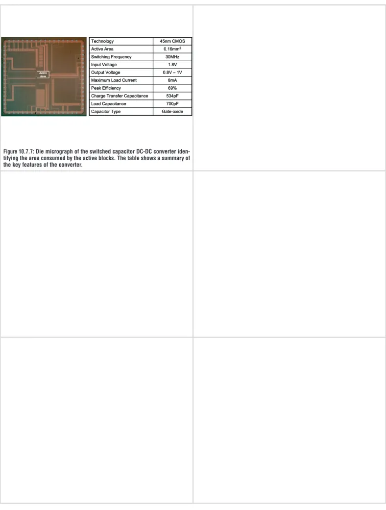
Figure 10.7.7 shows the die micrograph and performance summary of the 45nm CMOS test chip. The active area of the SC converter which includes the
charge-transfer and load capacitors is only 0.16mm2. All the capacitors used are
obtained using gate-oxide capacitors. References:
[1] L. Su, D. Ma and A. P. Brokaw, “A Monolithic Step-Down SC Power Converter with Frequency-Programmable Subthreshold z-Domain DPWM Control for Ultra-Low Power Microsystems,” ESSCIRC, pp. 58-61, Sept., 2008.
[2] Y. K. Ramadass and A. P. Chandrakasan, “Voltage Scalable Switched Capacitor DC-DC Converter for Ultra-Low-Power On-Chip Applications,” IEEE Power Electronics Specialists Conference, pp. 2353-2359, June, 2007. [3] J. Zeng, S. Kotikalapoodi and L. Burgyan, “Digital Loop for Regulating DC/DC Converter with Segmented Switching,” U.S. Patent 6,995,995, Feb. 2006 [4] G. Patounakis, Y. Li and K. L. Shepard, “A Fully Integrated On-Chip DC-DC Conversion and Power Management System,” IEEE J. Solid-State Circuits, vol. 39, no. 3, pp. 443-451, Mar., 2004.
209
DIGEST OF TECHNICAL PAPERS •
ISSCC 2010 / February 9, 2010 / 11:45 AM
Figure 10.7.1: A two-way interleaved G2BY3 gain setting to provide voltages below 2/3rdof the input voltage (1.8V). The total on-chip charge- transfer
capacitance used is 534pF (=64CB), and the load capacitance is 700pF.
Figure 10.7.2: Binary-weighted partitioning of the charge transfer capacitors and switches for digital capacitance modulation. C<0:3> turns ON or OFF the coarse blocks. F<0:1> controls the finer splitting of the 1CBcapacitor.
Figure 10.7.3: Architecture of the switched-capacitor DC-DC converter system. COMP3 compares VLwith a reference voltage VL_OFFwhich is generated
on-chip and is designed to be 100mV less than the required VL.
Figure 10.7.5: Measured load transient performance of the SC converter with COMP3 (a) enabled and (b) disabled for a load current change from 270µA to 7.6mA. The converter is in PFM mode when DCM/PFM is low and in COARSE mode when FINE/COARSE is low.
Figure 10.7.6: Efficiency of the switched-capacitor DC-DC converter with (a) change in load voltage while delivering a load current of 5mA (b) change in load current while delivering a load voltage of 0.9V from a 1.8V input supply. Figure 10.7.4: Flowchart showing the events leading to transition between FINE/COARSE modes of regulation and DCM/PFM modes of control. ‘N’ can be set to 4 or 8. VBAT 16CB Φ1 Φ2 Φ1 VBAT 16CB Φ1 Φ2 Φ1 Φ 2
G 2B Y 3
CL VL IL VBAT 16CB Φ2 Φ1 Φ2 VBAT 16CB Φ2 Φ1 Φ2 Φ1 VBAT 8CB Φ1 Φ2 Φ1 VBAT 8CB Φ1 Φ2 Φ1 Φ 2 VL C<0>, 8X VBAT 4CB Φ1 Φ2 Φ1 VBAT 4CB Φ1 Φ2 Φ1 Φ 2 VL C<1>, 4X VBAT CB Φ1 Φ2 Φ1 VBAT CB Φ1 Φ2 Φ1 Φ 2 VL C<3>, 1X VBAT 2CB Φ1 Φ2 Φ1 VBAT 2CB Φ1 Φ2 Φ1 Φ 2 VL C<2>, 2X FINE-SPLITTING CB VBAT CB Φ1 Φ2 Φ1 VBAT CB Φ1 Φ2 Φ1 Φ 2 VL FINE, 1X 4CB/7 CB/7 F<1> 2CB/7 F<1> F<0> F<0> COARSE FINE C<0:3> CL K COMP1 CL(700pF) VL VREF -ΔV VFB GO_UP CL K COMP2 VREF + ΔV VFB GO_DOWN MODE DECISION DCM/PFM FINE/COARSE ADD/SUB F<0:1> SWITCH MATRIX VFB NON-OV CLK GENERATOR CLK (30 MHz) PFM_PULSE DCM/PFM 0 1 VBAT (1.8V) Φ1 Φ2 CL K COMP3 VL_OFF VL COARSE_EN REF<0:2> PFM_PULSE LOGIC COARSE GO_DOWN GO_UP FINE C<0:3> = 0 GO_DOWN COARSE_EN DCM PFM C<0:3> = 0 GO_DOWN GO_UP N times FINE / COARSE DCM / PFM Yes Yes (a) (b) VL = 1V VL = 1V DCM/PFM FINE/COARSE 120ns 1.2μs DCM/PFM FINE/COARSEREF=‘000’ : IL= 270μA x 7.6mA REF=‘000’ : IL= 270μA x 7.6mA
0.1 1 10 20 30 40 50 60 70 80 IL(mA) Efficienc y ( % ) 0.75 0.8 0.85 0.9 0.95 1 20 30 40 50 60 70 80 VL(V) Efficienc y ( % ) 0.75 0.8 0.85 0.9 0.95 1 20 30 40 50 60 70 80 VL(V) Efficienc y ( % ) (a) (b) IL = 5mA VL = 0.9V Ideal LDO PFM DCM
10
• 2010 IEEE International Solid-State Circuits Conference
978-1-4244-6034-2/10/$26.00 ©2010 IEEE
ISSCC 2010 PAPER CONTINUATIONS
Figure 10.7.7: Die micrograph of the switched capacitor DC-DC converter iden-tifying the area consumed by the active blocks. The table shows a summary of the key features of the converter.
Active Area
534pF Charge Transfer Capacitance
700pF Load Capacitance
30MHz Switching Frequency
8mA Maximum Load Current
69% Peak Efficiency Gate-oxide Capacitor Type 0.8V – 1V Output Voltage 1.8V Input Voltage 0.16mm2 Active Area 45nm CMOS Technology 534pF Charge Transfer Capacitance
700pF Load Capacitance
30MHz Switching Frequency
8mA Maximum Load Current
69% Peak Efficiency Gate-oxide Capacitor Type 0.8V – 1V Output Voltage 1.8V Input Voltage 0.16mm2 Active Area 45nm CMOS Technology

![[PDF] Cours Algorithme Notions générales en PDF | Cours informatique](data:image/gif;base64,R0lGODlhAQABAIAAAP///wAAACH5BAEAAAAALAAAAAABAAEAAAICRAEAOw==)