A Design for an RGB LED Driver with Independent PWM Control and Fast Settling Time
by
Awo Dede 0. Ashiabor
Submitted to the Department of Electrical Engineering and Computer Science in Partial Fulfillment of the Requirements for the Degree of
Master of Engineering in Electrical Engineering and Computer Science at the Massachusetts Institute of Technology
May, 2007 ©2007 Massachusetts Institute
All rights reserve(
Author Department of Electrical EL May 25, 2007 Certified bv Certified by Accepted by vid Perreault] ;is Supervisor Arthur C. Smith Professor of Electrical Engineering Chairman, Department Committee on Graduate Theses
BARKER MAS$ACHUSETTS INSTiTUTE,
OF TECHNOLOGY
[John ily, Seniojn- ign Engineer) VI-A Company Thesis Supervisor
A Design for an RGB LED Driver with
Independent PWM Control and Fast Settling
Time
By
Awo Dede 0. Ashiabor
Submitted to the Department of Electrical Engineering and Computer Science on May 28, 2007,
in partial fulfillment of the requirements for the degree of Master of Engineering in Electrical Science and Engineering.
Abstract
A small sized and efficient method to power RGB LEDs for use as backlights in flat panel displays is explored in this thesis. The proposed method is to drive a parallel switched connection of LEDs with a single Average Mode Controlled buck regulator. Specifications for the switching regulator and control circuitry are described. The application circuit demonstrates current settling times between 7ps and 30ps at a switching frequency of 290kHz. Current settling is improved at higher switching frequencies, with settling times approaching a 2ps to 4ps range at 1MHz switching. M.I.T. Thesis Supervisor: Prof. David Perreault
VI-A Company Thesis Supervisor: John Tilly (Linear Technology Corporation)
Table of Contents
1. Introduction ... 7
a. Display Technologies of Today...7
b. The use of LEDs in Displays...9
c. A bout this T hesis...9
i. Minimizing the settling time of a Multiple LED driver...9
ii. Other performance criteria...12
iii. Thesis Organization...14
2. Overview of Design Strategies...15
a. Theoretical Solutions... 15
b. Commercial Solutions...24
3. Systems and Specifications...28
4. Design and Simulation...30
a. Average Current Mode Controlled LED Driver...30
b. Improvements to ACMC Controlled LED Driver...38
c. Modeling of External Components...54
d. Modeling of Power Dissipation...54
5. T esting ... . ..55
a. Measurement Techniques ... 57
i. Settling tim e... 57
ii. E fficiency...58
b. Performance on Breadboard...59
i. Settling tim e... 63
ii. E fficiency...69
c. Solution Integration in I.C. ... 72
6. C onclusion ... 74 a. Sum m ary... 74 b. C ontributions... 74 c. Future W ork... 75 d. Acknowledgements...75 7. B ibliography... 76 8. A ppendix I... 78 9. A ppendix II... 80 10. A ppendix III... 82
Table of Figures
1.1: DLP incorporating the fast current settling multiple LED driver...5
1.2: Fast settling output current allows faster frequency, a higher refresh rate and better contrast pictures on DLP screen...5
1.3: Traditional Multiple LED driver has distinct drivers encapsulated into one chip...7
1.4: Proposed Multiple LED driver with one output port serving multiple LEDs...7
2.1: Proposed Multiple LED driver with one output port serving multiple LEDs...9
2.2: 2-phase Buck converter. ... 11
2.3: Waveforms of the 2-phase Buck converter...12
2.4: Basic structure and operation of FRDB converter...13
2.5: Average Current Mode buck regulator...15
2.6: The principal difference between this current mode regulator and the voltage mode circuit is in the source of the modulating ramp. ... 16
2.7: LEDs driven by separate converters...19
2.8: Parallel topology... 20
2.9: Series T opology...21
3.1: Multiple LED driver...22
4.1a: Schematic of Average Current Mode Controlled LED Driver. ... 25
4.1b: Block diagram describing system during a reference current step. ... 26
4.1c: Block diagram describing system during a load step... ... 26
4.2: Transfer function of PWM comparator...27
4.3: Bode plot of open-loop buck and ACMC compensated open-loop gain ... 30 4.4: LED current settles to 5% of final value in 7ps in response to a reference current step ... . . 3 1
4.5: Transient response to a step in output current. Output current settles within 27pis to
5% of final value. ... .... 31
4.6: For a 2.4A step in output current, settling time is 80ps ... 32
4.7: The critical inductance design scheme keeps the small signal settling time at 7ps.. 34
4.8: After applying the critical inductance technique, the settling time for large output reference current steps improves from 80pts to 73ps. ... 34
4.9 After applying the critical inductance rule, the output current settling time stays at 27ps. ... .... 35
4.10: The anti-windup circuit reduces large reference current step settling time from 73pis to 22ps. ... 36
4.11: Slowly ramping up the reference current also reduces settling time from 73ps to 24ps. ...- --... 37
4.12: For a 2.4A reference current step, reducing output inductor to 20pH lowers the settling tim e further to 17ps. ... 38
4.13: Switching at 1MHz results in a 2ps settling time for a 600mA step in reference cu rren t. ... ... 4 2 4.14: And for a 2.4A step in reference current, settling time is 4ps. ... 42
4.15: At 1MHz switching, output current settling time is 7ps. ... 43
5.1: PCB board of initial design. ... 49
5.2: Full circuit schematic of the prototype system...50
5.3: The large ripple on the output current makes it difficult to spot the 5% settling time. After smoothing output current with a moving average, settling time is easily read off plot as 9p s. ... . . 52
5.4: RGB LEDs produce a white color. ... 54
5.5: RGB LEDs produce a green color... ... 54
5.9: SPICE simulation of experiment of Figure 5.8...56
5.10: Experimental results showing LED current settling time versus inductor size. ... 57
5.11: Experimental results showing LED current settling time versus output capacitor size . ... 5 9 5.12: Experimental results showing LED current settling time vs output resistor size....60
5.13: Experimental results showing efficiency versus output resistor size ... 60
5.14: Experimental results showing LED current settling time versus input voltage...61
5.15: Experimental results showing LED current settling time vs frequency...62
5.16: Experimental results showing efficiency vs. input voltage...63
5.17: Experimental results showing efficiency versus output current...64
5.18: Experimental results showing efficiency vs inductor size. ... 65
List of Tables
2.1: Tradeoffs of Theoretical solutions... 18
2.2: Tradeoffs of commercial solutions...21
3.1: Specifications for Multiple LED Driver... 23
4.1: Summary of design choices and settling times...44
5.1: Prototype operating parameters ... 51
Chapter
1
-
Introduction
a. Display Technologies of Today
Flat panel televisions are no longer a luxury item. Today, the average television store can boast of an eclectic stock of High Definition (HD) televisions, Liquid Crystal Display (LCD) televisions, Plasma Screen televisions and Digital Light Processing (DLP) televisions, to name a few. Sales of flat screen TVs alone hit a $17 billion figure in 2005, and are projected to continue on an upward trend. This boom in the television business is only a microcosm of a greater innovation in the display industry. Besides TV sets, we enjoy very fine, life-like pictures off minute screens in PDAs, cell phones and other tiny consumer portables. These novel displays are expected to permeate business areas too; there is good reason to believe that medical imaging devices will be upgraded to these sharper displays, and so will computers, spectroscopes, microscopes, 3-D visual displays, holographic storage devices, and professional photographic devices.
The new display technologies make up for the deficiencies of CRT technology such as its bulkiness and poor contrast in large screens. These innovative screens also deliver digital television which CRT cannot provide. Though the new screens are all improvements to the CRT screen, they each have their own setbacks, and as a result, it is still early to select one technology as the overall best. That is why we still see many types of flat screens on the market. We discuss a number of these screen technologies below.
Thin, lightweight and silent, LCD screens run on low power and provide good text contrast. They also offer a wide viewing angle and low electromagnetic radiation. What's more, since 1999, the prices of LCD sets have been declining steadily, largely, as a result of improvement in the LCD manufacturing process. The negative aspects of LCD technology include poor image contrast. LCD technology cannot create rich black colors. Its inherent fixed resolution, limited peak brightness, caused by the fixed brightness of the backlight, and its notorious motion blur makes the viewing experience less than heavenly. The size-cost ratio unfortunately remains prohibitively high, even though this ratio is on a downward trend.
Plasma screens also have many advantages comparable to the LCD: wide viewing angle, as well as a flat and compact shape. Moreover, there is no flicker effect' in plasma screens. Additionally, its architecture has no need for a backlight or a projection of any kind, making for very thin (albeit heavy) devices. Plasma screens also emit rich colors
that the LCD screens cannot match. That said, they do not come cheap.
The advantages of DLP technology include its light weight, high gamut of color, and excellent contrast ratios. Unfortunately, DLP screens require at least 12" -24" depth. This renders the monitors bulky. Furthermore, in single chip DLP systems, there is the potential of having the "Rainbow Effect". This problem is unique to DLP. A rainbow forms briefly in the viewer's peripheral vision. It occurs when viewers rapidly shift their
The use of LEDs in Displays
It is reported that replacing the fluorescent backlight with LEDs corrects the "rainbow effect" in DLP TVs [1]. Other screen manufacturers like Samsung and Acer are also installing LEDs as backlights in LCD screens, to improve (dynamic) contrast ratios and thereby enrich color production. Compared to CCFL backlit LCDs, LCD panels with LED backlights can easily be divided into subsections. The brightness of each subsection is controlled independently to produce many levels of brightness and with it, a high contrast ratio. LEDs also eliminate the warm-up time and color instability of screens since they have an instant turn-on. An additional advantage to consumers is that LEDs have longevity.
b. About this Thesis
i.
Minimizing the settling time of a Multiple LED driver
The intention here is to design a compact and cheap way to drive LEDs for use in flat panel displays. The key feature of this compact, cheap LED driver is its fast current settling. Allow me to explain why this property is important.
If one could develop a single affordable and small-size LED driver that could drive many types of LEDs, i.e. LEDs of different current ratings and forward voltages, one could eliminate many LED drivers in the display, replacing them with a single circuit that switches among several LEDs. In order for this multiple LED driver to be useful, the output current must settle to its nominal value quickly. There is no point in using a multiple LED driver if the current settles slowly. This is because the colors of the
different LEDs will reach the requisite hue slowly. If the colors settle slowly such that we have to cycle through these LEDs at a frequency lower than 100Hz, the eye will be unable to blend the distinct colors. The ability to blend colors to form a wider spectrum of colors is lost. Evidently such an LED driver is inappropriate for lighting applications.
In the DLP screen for example, a driver could drive RGB LEDs in the backlight. In a given cycle (at a frequency higher than a 100Hz), the driver turns on the red LED for 30% of the time, the green LED for another 30% and the blue LED another 30%. Because the red, green and blue LEDs may require different forward voltages and current, our multiple fast settling LED driver must reset its output current and voltage quickly each time we switch between the LEDs. See Figure 1.1. When the red, green and blue lights reach the DLP chip, they are pulse-width modulated. The red light may hit the DLP chip first and is reflected onto the screen for the required amount of time to illuminate the right amount of red light. The green light may hit the DLP chip next and may be reflected for a different amount of time. The blue light then follows and may also be sent to the screen for a different duration. If the red color is reflected onto the screen longest, the resultant color appears reddish, if the blue light is reflected for the longest duration within a cycle, the resultant color appears bluish, and so on.
Driver Ouput Voltage/Current
Screen
GREEN RED RED I I BLUIE T DLP Chip A MaodationiJi timeII
T timeFigure 1.1: DLP incorporating the fast-current-settling multiple LED driver. voltage and output current are reset whenever we shift between LEDs. In the first dominant bluish color is produced.
Output
cycle, a
This technology is suitable only if the RGB currents settle fast, otherwise as Figure 1.2 depicts, we cannot cycle through the three primary colors at a rate faster than a 100Hz. The human eye will see the distinct red, green and blue colors, rather than one integrated color [2]. LED drirer Output Current -4 R G B R Slow Settling SG B R G B R G B R G B R Fast Settling 0 loms 20ms time
Figure 1.2: Fast settling output current allows faster frequency, a higher refresh rate and better contrast pictures on DLP screen.
Multiple LED Driver
F---I
IMUZD LP chipThe benefits of using our small-size inexpensive multiple LED driver in DLP screens are plentiful. First, we eliminate the color wheel and all the mechanical circuitry involved in combining color. We shrink the size of the DLP screen as a consequence. We can also guarantee a longer life for the screen due to the longevity of LEDs. The screen runs on lower power because one, LEDs are more efficient than white lamps and two, because we eliminate the color wheel. The color wheel in DLP TV wastes a lot of energy in its operation. To create non-white colors, it filters out the unwanted color components of the white light. The light components that are filtered out are wasted in the form of heat energy. Also, if the output current settles very quickly, we can cycle through the LEDs at a frequency much higher than 100Hz. DLP manufacturers claim that there are many advantages associated with operating at higher frequencies [3]. That is why we place enormous emphasis on the fast current settling characteristic of our multiple LED driver.
ii. Other performance criteria
Traditionally, what we term as a multiple LED driver is in fact several distinct LED drivers packaged into one chip. This multiple driver is characterized by several distinct output ports illustrated by Figure 1.3. The idea is that if we could create a real multiple driver, that is, a driver with one output port serving multiple LEDs, we size down the LED driver and possibly its cost by a great margin. Compare the traditional multiple LED driver in Figure 1.3 to the proposed multiple LED driver of Figure 1.4.
Vf1
Driver 1
1Driver 2 --
12
1-7-/~ 3
Figure 1.3: Traditional Multiple LED driver has distinct drivers encapsulated into one chip.
Drive 13
Figure 1.4: Proposed Multiple LED driver with one output port serving multiple LEDs.
In addition to a smaller sized solution, we seek a driver that is efficient and beats the efficiency or at least matches the efficiency of existing lighting solutions. The more efficient the system, the less costly it is to operate, since it expends less energy. The efficiency of the system also impacts the size of the solution. A grossly inefficient
lighting system will demand larger heat sinks and will make the screen very bulky and unattractive for use in flat panel displays.
We see this fast current settling multiple LED driver playing a major role in all applications that require fast settling multiple output currents. Its use is not limited to display applications.
iii. Thesis organization
Chapter 2 of this thesis presents an overview of several design strategies and considerations for multiple LED drivers.
Chapter 3 presents the specifications of the multiple LED driver.
Chapter 4 is a rigorous discussion of the design selected for the implementation of the multiple LED driver.
Chapter 5 describes methods used to test a prototype built from discrete components and presents a summary of the results obtained on the bench.
Chapter 6 summarizes the concepts learned from this thesis and proposes future work. Chapter 7 is a bibliography of references cited in this thesis
Appendix I contains the circuit description in SPICE.
Appendix II contains the MATLAB code used to simulate the circuit.
Chapter 2- Overview of Design Approaches
a. Theoretical Solutions
There are a number of recommendations pertaining to fast transient DC/DC converters which apply to the design of the multiple LED driver of Figure 1.4, repeated here as Figure 2.1. In recent years, some designers have proposed means of increasing the bandwidth of the systems and some have even proposed changing the inherent topologies of the converters. We discuss a few of these schemes: switching at higher frequencies, multi-phase converters, the fast response double buck converter (FRDB), the average current mode control scheme and the peak current mode control method. In the next few pages, we examine each proposition closely to select the most suitable scheme for the
work at hand -a compact and efficient fast current multiple LED driver.
Driver
1
SI S2+IS
Figure 2.1: Proposed Multiple LED driver with one output port serving multiple LEDs.
Switching at higher frequencies
A high switching frequency means that the control loop of the system is able to correct errors more rapidly. The output current as a result will settle to the correct value quickly. Another benefit of switching at a higher frequency is a reduction in the output ripple.
This means that one can get away with smaller and inexpensive filtering devices at the output node. Indeed, these advantages do not come at zero cost. Higher switching frequencies cost efficiency. Since some components' switch power loss are proportional to frequency, higher switching frequency translates to higher power losses. Also, when one switches at a higher frequency, one runs into noise coupling issues and the layout design is greatly complicated.
Multi-phase converters
Multi-phase converters work by interleaving more than one distinct converter operating out of phase with each other [4], [5]. The purpose is to reduce ripple on the output without using massive filtering elements at the output stage, which slow down the settling of the output current. By avoiding big inductors and capacitors, the output responds more quickly to changes in the system than it would otherwise. Multi-phase converters produce low output ripple and fast settling current. It is for among these reasons that the multi-phase synchronous buck converter has become the dominant topology for
via ~-I LI
VS1
L2 C~ VoutFigure 2.2: 2-phase synchronous buck converter. Adapted from [7].
Consider the two-phase converter of Figure 2.2. Assuming that the size of the inductors Li and L2 are the same, and that the gate signals VS1 and VS2 are exactly 180 degrees out of phase, and that the system is operating near 50% duty cycle, the current through LI and L2 will resemble that drawn in Figure 2.3. As shown in the picture, the resultant output current has only small ripple, with a fundamental frequency of twice the switching frequency of each power stage. For constant total energy storage, interleaving N stages reduces ripple current by a factor greater or equal to N and increases fundamental ripple frequency by a factor of N [4], [5].
IVt
T tn
Figure 2.3: Waveforms of the 2-phase synchronous buck converter.
This implies in turn that the designer can generate an output current having a given ripple
with reduced inductors and capacitors as compared to a single power stage. Moreover, because the individual inductors are small, one can slew the operating current quickly compared to a single buck converter with the same ripple current. Additionally, because we now have essentially two buck stages, we spread the power consumption across more converters. This distribution allows the chip to withstand larger total power consumption.
One problem with the multi-phase converters is that we add another layer of complication. That is to say, we have to carefully synchronize the gate signals to avoid an open at the input, significant delays, and uneven power sharing [8]. Our layout is also made complex. In this thesis, we focus on a single-phase design, but recognize that a multi-phase approach may be valuable in some applications.
Fast transient response dc/dc converter
converter are identical, converters of the fast transient buck are not identical. The two converter stages in the "fast transient response" converter have different functionalities. The linear or main buck converter operates like a typical buck converter. The novel addition is the second "auxiliary" stage. What does it do? Because the output filter is a low pass filter, it removes all high frequency components at the output. By so doing, it limits fast transitions at the output. The purpose of the auxiliary stage is to inject extra current to speed up such transitions at the output, while maintaining low output ripple. See Figure 2.4 for a block diagram of the circuit.
If Fast Response Transient Operation Auxilliary.Switching -- Converter-. Main Source Load Con-rerter Slow Steady Im State Operation
Figure 2.4: Basic structure and operation of FRDB converter. Adapted from [9]
The sum of the filtered output of the buck stage plus the injected current from the non-linear converter provides a fast transient, low ripple response at the output. In principle, if the two power stages operate independently of each other, there is no stability issue if
each control loop is independently stable.
It should be recognized that the control of the auxiliary converter is not trivial. How much current should it inject or take out during a step of the output current? Since our
application calls for a variable output current step, the control of the auxiliary converter must be dynamic as well - a nontrivial exploit. For reasons of complexity, this design strategy is not considered further.
Average Current Mode Control
We have held a discussion of a few relevant topologies. Let us describe how the control scheme can influence the transient response of the driver. We first take a look at the Average Current Mode Control, (ACMC) [10]. ACMC is popular for its simple feedback technique. The control consists of two loops. There is a fast internal current feedback loop and a slower voltage feedback loop. The fast current feedback circuit measures a low-pass filtered version of the inductor current and compares it to an error signal generated by the slower voltage error amplifier. The signal from the current error amplifier is fed to a PWM comparator whose other input is a sawtooth ramp. This PWM comparator produces a pulsating signal. The duty ratio of this signal serves to modulate the output power. When output current is too low, the duty ratio of the pulse increases; as a result, the converter switch stays on for a longer time period, and consequently, the output power ramps up. When output current is too high, the converse occurs. Via this feedback, the circuit maintains output voltage and current at the prescribed value.
-Vot
+ ELo
COCPKAT NRAR
Figure 2.5: In this Average Current mode buck regulator, the error signal and a modulating ramp form a pulse-width modulator, which controls the buck switch.
In order to generate fast transient responses and accurate output, the control path is made fast by proper dynamic compensation of the (current) error amplifier. By providing full state feedback (of both inductor current and capacitor voltage) better dynamics are
achievable than can be obtained with a voltage feedback alone.
Peak Current Mode Control
Similar to ACMC, under Peak Current Mode Control (PCMC) one utilizes feedback of both inductor current and capacitor voltage to improve dynamic performance. What differentiates the two modes is the origin of the modulating ramp. Under PCMC, the modulating ramp is a signal proportional to the buck switch current, or equivalently, the inductor current. Each cycle, the switch is turned on, and then turned off when the inductor (or switch) current reaches a peak value set by the voltage loop. An additional modification is that a compensating ramp is also sometime required to prevent subharmonic oscillations [11].
Vout Voltage Loop SRIERENCI Vi-DRAVIR v
I
~ COMPARALOR SANUCH Q R AEASURE CLOCKCurrentFigure 2.6: The principal difference between this current mode regulator and the voltage mode circuit is in the source of the modulating ramp. Adapted from [10].
Evidently, for PCMC to run correctly, it requires an accurate yet fast measurement of the inductor current to create the modulating ramp signal. This measurement is no trivial feat. One could capture the buck switch current. The mechanism draws on the fact that when the buck switch is on, the inductor current equals the switch current. Other measurement choices include placing a sense resistor in series with the inductor, a current sense transformer across the on-resistance of the switch, or a current mirror circuit coupled to the switch. Each of these methods requires a level shift to transpose the measured signal down to the ground reference for application to the PWM comparator, since the buck regulator modulating switch is floating. None of the switch's terminals is connected to ground. The source terminal of the switch is either at the input voltage potential when the switch is on or at approximately 0.7V when off.
One perceived advantage of Average Current Mode Control over Peak Current Mode control is noise sensitivity. As the comparator is driven from the wide-bandwidth current sense, there is the potential for noise to trigger the PWM comparator. Under Average Current Mode control, only a low pass filtered version of the current is sent to the PWM comparator, providing noise immunity. Conversely, however, Peak Current Control provides "instant" pulse-by-pulse current limiting, where Average Current Mode Control does not.
Another advantage of Average Current Mode Control over Peak Current Mode Control is accuracy. Since the output current is exponentially dependent on the output voltage in the LED driver application, it is extremely important that the reference voltage setting the output voltage is precise. Furthermore, because the multiple LED driver of Figure 2.1 is designed to drive many LEDs of different forward voltages, over different currents, the output voltage is expected to step to several different values. Thus, the reference voltage must accurately predict the output voltage needed for the many LED types and output currents. In order to keep the control scheme for the driver of Figure 2.1 simple, a single (current) loop control method is considered in which one directly regulates the average output current. Both the ACMC and PCMC if used, will be stripped of its voltage loop entirely. A one (current) loop ACMC control without the voltage loop, still regulates the average output current with remarkable accuracy. However, PCMC without its voltage loop, regulates the peak output current. Additional circuitry needs to be added to remove the peak to average current error. This supplementary circuit further complicates the PCMC control circuitry.
Table summarizing
Property\Topology Multi-phase FRDB
Transient Response Fast Fast
Efficiency Moderate Moderate
Ripple Current Depends on number of Low
phases and duty cycle.
External High High
Component count
Die size Big Big
Total cost High High
Property\Control ACMC without voltage loop PCMC without voltage loop
Transient Fast Fast
Response
Noise sensitivity Low High
Accuracy High Low
Table 2.1: Tradeoffs of theoretical solutions.
Considering our evaluation of the solutions at hand, it appears that the most likely successful candidate is a single synchronous buck power stage employing average current mode control. The reason behind this choice is that a single buck power stage will enable the basic approach to be tested out with the greatest simplicity. This could be extended (e.g. to a multiphase interleaved design) later if higher performance is deemed necessary. ACMC provides the best combination of precision, fast transient response and low noise.
b. Commercial Solutions
Here are some examples of ways that manufacturers design power converters to generate multiple fast settling currents.
Separate topology
One solution in industry is to drive the individual LEDs with separate converters from one power supply. There are n converters for n LEDs. Each converter provides the right amount of current to its corresponding LED. This topology does not demand fast settling currents, since the LEDs are on the entire time that the driver is on. The problem with this solution is that the size of the die is large and numerous inductors are required. Consequently, it is an expensive solution.
VIN .... (N)
VD, VDN
I ID
*(N-+1) pins
Figure 2.7: LEDs driven by separate converters.
Parallel topology
Here, one buck stage serves one distinct output node connected to multiple LEDs. The output voltage is modulated, but the different currents are set by the resistors added onto the LED strings. The resistor size controls the voltage across the LED, and by so doing, it fixes the LED current.
IN a V 0 _ (N)
se
a aVDI VDN
y VDN
sasN
Figure 2.8: Parallel topology
Gate signals sent to switches S, through to Sn turn the LEDs on and off almost instantaneously. Because the parallel topology uses fewer elements than the separate topology, it is a much smaller and less costly solution. It is moderately efficient. The power wasted by the resistor ballasts aggregate to a significant sum that raises concern.
Series topology
Like the parallel topology, the series topology has one main converter stage. However unlike in Figure 2.8, the LEDs are connected in series. There are n switches. Each is connected in parallel with one LED. When a switch turns on, the diode is shorted out and is turned off. One big challenge here is the switch implementation. It will require level shifting since only one switch is referenced to ground. All the others are referenced to a varying voltage. Even though the die size appears smaller than that of the separate topology, the complicated switching circuitry increases the die size considerably, and
Tales mmrizin tradmumfs
Trnsen Respons Fas 40ftf Fastt0Ma t 0f Moderat
V IN
Switch sVD]Sith i Swic1 i
40 404 04 04 a 0
VDN* SI
Tota~ Hig Lfw Nos Mmderate
Iniua 2.ED Yesie YesoloNy
Curnt Ajsal
Die ~ ~ sieCnrlbgCnrlsalCnrlmdrt
Swtc s a awtc bi Swtc bi
Toa aotHg owMdrt
Iniiu LE Ye YeaN
-Crrn Adutbl
Table 2.2: Tradeoffs of commercial solutions.
The parallel topology appears to be the best suited to our purpose.
In conclusion, an ACMC approach with a parallel topology without the ballasted current sources may best answer our quest. A one loop, current loop ACMC will be used. This is because we expect the output voltage to vary a lot as we switch between several LEDs
and also vary the output current. This makes it difficult to pin an output reference voltage for the voltage loop.
Chapter 3
-
Systems and Specifications
Given the tradeoffs described in the preceding chapter, the best compromise between speed, size, cost and efficiency is to operate a single central control switch with one output node that sources several LEDs. These LEDs will be individually controlled with separate pulse signals (PWM). Since the different LEDs may require different DC output currents, the reference voltage that sets the output current will be pulsed to different voltages any time we switch between LEDs. The control circuit will adopt the single current loop Average Current Mode Control, which we shall loosely refer to as the Average Current Mode Control (ACMC).
OUTFIT Vin
TT
DRI
XLDI LEWN FEEDBACK CONTROL REFERENCEJ l
ti t2 t2 t3 t3 t4 ti t2 t3 t4Figure 3.1: Multiple LED driver
The gate signals S1 to SN and S do not have significant overlap. However, because they are being switched at a very fast frequency, the eye averages the independent colors into
has a low forward voltage. (One could select a different device or just use a "shorting" fet to tradeoff loss for output voltage deviation.)
Below is a set of practical electrical operating conditions at which we expect the multiple LED driver to meet. These requirements are based on commercial requests.
Multiple LED Driver
PARAMETER MIN TYP MAX UNITS
Input Voltage 10 15 30 V
Settling time 1 10 30 ps
Switching Frequency 0.15 0.6 2 MHz
Switch Duty Cycle 0 95 %
Output Current 0 3 A
Output Current ripple 150 mA
Output regulation 1 4 %
Quiescent Current 5 6 mA
Reference Voltage 0 1.25 V
Efficiency 85 92 %
Chapter 4 - Design and Simulation
Because of time constraints, the circuit is designed and implemented using discrete components instead of in an integrated circuit. There is good reason to believe that the results obtained from the breadboard will provide great insight into a design on transistor level. This section explores how to achieve fast settling time with an ACMC controlled multiple LED driver based on a synchronous buck. Some suggestions to improve the settling time are also presented. This is followed by a discussion on the limitations of these design choices.
a. Average Current Mode Controlled LED Driver
Shown in Figure 4.1 a is the simulation schematic of an ACMC controlled multiple LED driver. The output stage of the buck is a simple low-pass LC filter. The driver is
designed for fast transient response at a 290 kHz switching frequency without exceeding the ripple specification (maximum 150mA peak to peak output current ripple). Specific circuit values and tradeoffs will be discussed in the following text.
Voic R2 Current Sense Ri U2] R3 <9.2K < -a Lot Res Vin U- SW \/ C1 e .0i ___3P ou R12 .. MBR74S LUWLEDG -- DI CoUtB R17 T~~ - 1P 3 1/ D4 DT Vout Rio RI1
t11
t
DO LUJILEDG LUMILEDG RU R16 3 G0JlFDS6670A 1/S FDSG67OA D2 RIO C PM Comparator 7 jLT1192 Vca >U1 M ~ D3 R20 U5 Va Vsaw ; -1 R8 SD4US 20k LT1 182 > RS A2 R5 A3 A4 12k U7S R9 L$ CLOCK LT19 MI 107 op 2.2n 4.7k Sawtooth Generator Clock generator Compensator Ci 22-p Ri Rf Cz 1k 14.7k 338p PTi3it ef Rref I rek Pre4iilter > V2--
)
M >V4 > V9 > VS , i 15 LV5 V10 4.5 -4.7 3 3 1/1 DO SAl ASA1O All 100 -N VCC BOOST - - 1
:R j* Q* 4
UMP TG C2
RI V1422L R VN222LL m LTC4410-5 '
(7
T O 0122SR-LATCH OND TS g
Eliminate effects of noiselringing
Gate Driver
Figure 4.1a: Schematic of Average Current Mode Controlled LED Driver. See Appendix I for circuit description in SwitcherCAD.
-Buck
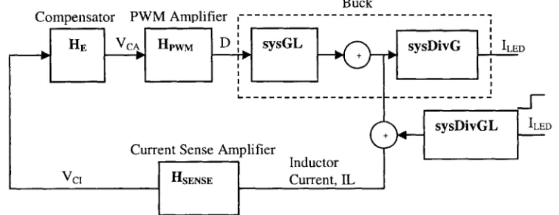
Compensator PWM Amplifier
---HE Hwm D sysGL sysDivG 'LED
Current Sense Amplifier Inductor
VC1 HSENSE Current, IL
Figure 4.1b: Block diagram of Average Current Mode controlled multiple LED driver.
This circuit is for a step in reference current. See Appendix II for block descriptions in MATLAB.
Buck Compensator PWM Amplifier
HE C Hpwm sysGL sysDivG ILE
sysDivGL 'LED
Current Sense Amplifier
VC1 HSENSE Current, IL
Figure 4.1c: Block diagram of Average Current Mode controlled multiple LED driver. This circuit is for a step in the load. See Appendix II for block descriptions in MATLAB.
Figure 4. 1b shows the control block diagram of the system. IREF sets the output current.
R 2
The inductor current sensed by HSENSE = Rsense * - gives Vci, which is compared to RI
IREF at the compensator. The difference is multiplied by the compensator transfer
sRfCz +1
approximation HPwM stems from the assumption that VCA is a DC signal. Suppose this assumption is accurate, as Figure 4.2 below illustrates, the duty cycle D can be
approximated as VcA/(VSAW*fSW) since VCA = SAW
D T
VSAW
VCA
A A
0 D T 2T 3T
Figure 4.2: Assuming VCA is a constant, the transfer function of the PWM comparator can be linearized.
The next block mod
multiplies sysGL ~
els operation of the buck converter. At the buck, the duty cycle
INIRoUT
VNL
C ROUT L -to give the inductor current. A fr
s2*LOUT *COU +S* OUT +
ROUT
l+s*C *R
of the inductor current determined by sysDivG = OUT OU , flows into 1+ S * COUT * (ROUT + RLED)
the LED. RLED is the dynamic resistance of the LED. For our purposes, the value of the
dynamic resistance is in the range of 0.02M and 0.6 Q.
Figure 4.1 c shows a linearized model of the system during a load switch. Arguably, this model is flawed in many respects, however it provides an insight into the dynamics of the system during a load switch. The assumption is that the dynamic resistance of the LED and the output voltage are almost constant such that sysGL and sysDivG remain constant during the load switch. The idea behind the model in Figure 4. ic is that when the load switches from an LED to another diode of a different forward voltage, the output current
will jump or drop instantaneously primarily because of the exponential relationship between the output voltage and output current. This is valid if we assume the output voltage remains relatively constant at time t=O when the load steps. This change in output current is reflected in the inductor current via sysDivGL, a current division of the output current. SysDivGL = sROUT COUT +1
S 2LOUT CoUT + sRou COUT +1
In seeking the "fastest" transient response, we mean the fastest 5% settling of the output current to, one, steps in the reference current, characterized by a step in IREF in Figure 4.1 a and 4. 1b, and two, a load (or LED) switch at the output. Solving for the settling time
exactly involves very involved non-linear calculations. In order to avoid detailed
computation, we design for the highest possible bandwidth and a decent phase margin, a phase margin in the vicinity of 60' using linearized models and MATLAB as a tool. With the aid of SPICE simulations the settling time is calculated more accurately.
While filtering out ripple at the output, we jeopardize our mission to achieve a high bandwidth. The large filtering components we select for the output ripple attenuation present low frequency poles to the system. Without any dynamic compensation, these low frequency poles drag the bandwidth of the system to a low frequency too. The role of the compensator is to provide sufficient drive to compensate for these low frequency poles. The consequence is a higher bandwidth and faster settling. However, it needs to be recognized that the control authority to rapidly slew the output is limited by the inductor
system to changes in system parameters such as input voltage, output voltage and component values. With this compensation scheme, the buck stage parameters have limited impact on the small-signal bandwidth, though large signal changes are still (slew-rate) limited by the components. For simplicity, however, the design of the power stage and the controller are decoupled and designed sequentially. These design decisions are then studied and revisited where needed.
Initial Design
The output stage of the buck is constructed using a 33pH inductor and a 1 pF capacitor in series with a 1M damping resistor. This initial design adequately filters out the output ripple. Figure 4.3 confirms that this choice of output filter attenuates output ripple sufficiently. But the small-signal bandwidth is fairly low, meaning that the transient response of the open-loop buck is not fast.
Bode Diagram
J1U - - -t IL J JJ .- -U -J - L A -- - - ta J - -Z L -L J -1 J Iul - J -_J-L L L;_ U.
$i f I I I I I: It 1 I a 9 111 1 1 1 i i11111
+- -+ ----. --- .- AC C'ompensated - -- - - -- H-
-'I t Loop Gan |111 1 1||'I~~
n r TT r I - --T T -: r i T:l -- -r - i I T 1 1 1" .1 -1 r r r -1
Buck i l I i
I I I I I I t i l l I I I I I i 1 11, U -- 1 -1 1 11 ILI I LU i i -- i ii I iiiii Z- t i tiiI(
I Et i I i l 1i I I i ! I I I I I II i i i I I I l i tI
t ~ ~ ~ r isi a eei ' 1 t ii 1 -T; 'r 1| 1, Tti i r r r ell i n
-i -i -il 1 i i~ 1 1 i i i i t 1 l 1 1 1 1 1 1 i5 i i i e i i t -fill A I I I I T r iJ -7 T ACMC CompensatedI:; I 1 --- - - - - -J- L - - - -: - --.- ' J - -, - - - -10 10 1 Frequency (H z) 10 10
Figure 4.3: Bode plot of open-loop buck (= sysGL*sysDivG) and ACMC compensated open-loop gain (= sysHE*sysHPWM*sysGL*sysDivG) from MATLAB.
Compensation shifts bandwidth from 5kHz to 110kHz. The values used in the converter and compensator are
and
1.373e-39s7 + 2.72e-3 s6 +1.676e 27s5 +3.3e-22S4
9.245e~45s8 +1.374e-38s7 + 6.948e-3s6 +1.263e2 7s5 + 3.432e-23s4
1.848e 7sI + 4.035e-2 s7 + 2.999e-29s6 + 9.026e-34sI + 9.029e-39s4
(1.128e -s + 4 .527e 29s14 +6.826e s0l +4.599e-"s1 +0.01186s" +1.457e's 10 + 4.931e" s9 + 5.348es17S + 2.388e23S7 + 4.085e28s6 + 1.131e33s5 + 1.09e36s4)
respectively. The computation of these transfer functions is indexed in Appendix II.
ACMC modifies the slow small-signal behavior of the open-loop buck regulator by
injecting a zero before the switching frequency. This compensation is implemented as a type II compensator. With the driver powered by a 1OV input voltage and switching at 290kHz, the result is a 7ps settling time response to a step in reference current (at a constant 1Q load), and a 27ps settling time when we change the load from a Schottky
I' C 40 20 0 -20 0 U) Cu -130 -270 ACMC
340mV- 320mV- 300mV- 280mV- 26OmV- 24mV- 220mV- 200mV- 180mV- 160mV- 140mV- 120mV- --- --- -- --- -- - --I I I I
100MV
1
1
360ps 380ps 400ps 420ps 440ps 460ps 480ps 500Ps 520psFigure 4.4: LED current settles to 5% of final value in 7ps in response to current step. Upward settling time and downward settling time both equal 7ps.
54 a r V(vout] .0V -L- - - -- - - -- - - --- - --- - --- --- -- -- --1 DV-LED Switch ON -V- --- - --- --4V --- -- -2V - - - - - + - - - - --- --- - - - I(LIED ) -j---- - - - - -- -DV --- --- ~--- --- --2V- I 190pjs 21Otis 230ps 25ups 91 BmA -840mA -770mA -700mA -630mA ~56OmA 49OmA -420mA -35OmA 280mA 21 DmA -140mA - 70mA Ops eference 49OmA 39OmA 29OmA 19OmA 9OmA -1 DmA
Figure 4.5: Transient response of output current when load is changed from a Schottky to an LED of approximately 3.9V drop. Output current settles within 27ps to 5% of final value.
Since the RGB driver is to be used under varying duty cycle operations, it is important that the settling time remain reasonable for all possible reference current step amplitudes. We subject the driver to a 10% to 90% step in reference current and examine the current
settling. With this large reference current step, the settling time deteriorates considerably. This phenomenon occurs for reference current steps greater than 0.9A. As Figure 4.6
depicts, this slow reference current settling stems from duty cycle saturation. When the ------- --- ~- --- -- --- ------- -- - - -- - --- ---~- -- ---- --- --- --- -~~ - --- --- --- --- --- ---~-- --- - - - - --- - - -- - -- - - --- ---- ------ -- - ---- - --- --- -- ---- ---- - -- -- --- - .. .. .. ... .. .. . .. . .-.. - - - -- - --- - --- - - -- --- ---- --- - --- --- - --- -- -- -- -- -- - --- -- --- -- --- -~ ---- - -- -r - - -- ----- - -- - - -- - -- ----~- ~- ---- --- - --- - --- --- --- ---- -- -- -- -- -~-- -- - - --
-
---z2I ps 29IIsreference current makes a huge jump suddenly, the system falls out of small signal operation. Consequently, the settling time is no longer determined by the small signal bandwidth of the system, but rather, the settling time is dominated by a large signal slew
rate, which is closely related to the passive component values.
1.3V- .3.6A 1 1V---.--Ire -.9V --- - )--- - -- -- 2.A 0 .5 - -- + - --- -- - --- --- LE --- --- -- -- - - 1 2 0.7V - ---- -- -- --- 4--- --- 6---4--- -- -- - - --- -1.8A 0.1V- -0.DA
Buck switch ON/Duty Cycte
14 - p --- s ------ 4----0 s 80p 3 0
---
-- ----Figure 4.6: For reference current excursions beyond 0.9A, the duty cycle saturates and settling time worsens dramatically. For a 2.4A step in output current, settling time is 80ps compared to 7ps when reference current steps by 500mA.
In summary, settling time is 7ps in response to small reference current steps, 80ps in response to large reference current steps and 27ps when load is changed from a Schottky of approximately 0.2V drop to an LED of approximately 3.9V drop.
b. Improvements to ACMC Controlled LED Driver
We now explore the limitations of the initial design. Armed with an understanding of where the limitations stem from, we can improve the settling time by fine-tuning our
Improving small reference current step settling
The first item for improvement is the small reference current step settling time. In [12], P-L. Wong et al. (2002) describe a design method, critical inductance design, as a means to design a fast transient and efficient converter. The authors of Critical inductance in
voltage regulated modules claim that in a fast DC/DC converter, there exists a critical
inductance above which the transient response of the converter is drastically degraded. The idea behind the critical inductance is that as long as one avoids duty cycle saturation, by limiting inductor size to the "critical inductance", the converter exhibits superior transient performance compared to other conventional design methods such as the continuous conduction mode (CCM) or quasi-square wave (QSW) design. Typically, the critical inductance design solution yields a faster transient response in comparison to the other design schemes, and where the transient responses are comparable, the critical inductance technique offers lower output ripple. The authors of [12] define the critical inductance, LCRIT as the largest inductor that permits the largest needed change in duty
AD *V/ *;rI2
cycle. LCRIT- MAX IN ; ADMAX is the maximum change in duty cycle, AIOUT
AOUT *OBW
is the corresponding change in output current, VIN is the input voltage and OBW is the
bandwidth.
Given that our application calls for a ADMAX~O.9 5, AIouT~2.85A, 0OBw= 2n*29kHz at VIN=IOV, LCRIT calculates to be a 29pH inductor.
With LOUT at 29ptH, the output capacitance is set at 1pF, so as to meet the ripple
specification. The damping resistor is maintained at 1Q. The small reference current step settling time stays at 7ps and the output current settling time stays at 27pts. Meanwhile,
for large reference current steps, the settling time reduces from 80ps to 73ps. Figures 4.7 through to 4.9 illustrate these results.
44OmV- 1.04A
220mV- -- --- - --- 0.60A
OmV- Duty Cycle 0.16A
HV
4 V 7-
-I9ps 2 03ps 21 231ps 241ps 259ps
Figure 4.7: The critical inductance design scheme keeps the small signal settling time at 7ps. 1 V - - --- --- - - - --- 3.OOA OV- 0.04A Vjvea] vivsaw) Dutv evele Figu---:
-.---
HII--IIUH KJ
SDSwitch ON
oV -O-.3A
- - - - -- - .2A
V - -- -- ---- ----
-190p1s 200ps 21 tpls 22011s 230p1s 240ps 250ps 260pjs 27l0ps 280p1s 290ps 300p1s
Figure 4.9 After applying the critical inductance rule, the output current settling time stays at 27pis.
The critical inductance design method does not improve the small reference current step settling time. This raises the question as to whether the 29pH inductor is the true critical inductance. Suppose 7ps is the optimal small reference current step settling, it implies that the critical inductance is not 29pH but rather is an inductance equal or greater than
33piH. For, with a 33pH inductor, we still managed to avoid duty cycle saturation.
Improving large reference current step settling
Although the critical inductance design method is said to prescribe an inductor size such that duty cycle saturation is avoided, contrary to expectations, Figure 4.8 points out that the saturation problem persists for large reference current steps, even after the conservative critical inductance design. This apparent controversy is resolved by examining the root cause of the duty cycle saturation. It turns out that the duty cycle saturation observed in Figure 4.8 is not directly related to the output inductor size. The saturation here is different from that which is referred to by [12]. This saturation arises from the slewing of the integrating capacitors at the compensator. As Figure 4.8 depicts,
when the reference current steps, signal VCA, the compensator output voltage, swings to the supply rail immediately. Afterwards, the large integrating capacitors slow down the slew of VCA. It takes over 70ps slewing down to meet with the sawtooth signal, VsAW.
Even at time 680ps, 30ps after the reference current steps, the duty cycle wrongfully remains at 100%, although the output current has overshot its target -all because the slow slewing VCA is still well above the sawtooth.
One workaround is to add on an anti-windup circuit [13]. Two zener diodes connected back to back across the compensator capacitor Cp serve to clamp the integration error of the compensator, and prevent VCA from hitting the rails. Similarly, the amplitude of the sawtooth can be increased to reduce the voltage potential between the supply rails and the sawtooth. When a 4.7V zener anti-windup circuit is added, VCA clamps at 4.7V. The
settling time drops down to 22ps. This settling time is much better than the settling time attained by the initial design and the settling time attained by the "critical inductance" circuit. This improved settling is captured in Figure 4.10.
Iref I(LIED)
Duty Cycle
---An equally efficient remedy is to filter the reference current (or voltage) with a low pass filter. The compensator sees a smoother jump in the reference current (or voltage), and so does not provide needless gain that sends the output current overshooting its target. Figure 4.11 shows that by smoothing the large reference current step, the delay caused by the slewing of the integrating capacitors is truncated to 28pts.
Vjvsaw] jva 18V -- - - - -Duty cy ne Ire I I I I 0 . V -- - -- - -- --- -- --- - - - - ---- - ---- L - - - -- - -- - - - -- - --- -- - - -- - - - -1 3 ---- -40pis 50ps 60ps 70ps 80ps 90p.s 100ps 110ps 120ps 130ps 140ps 150is 160ps
Figure 4.11: Slowly ramping up the reference current also reduces settling time from 73ps to 28ps.
Figures 4.10 and 4.11 beg the question as to whether we can shrink the duty cycle
saturation time further, possibly to zero microseconds. We expect that by using a smaller output inductor, we can use smaller integrating capacitors, and as a result speed up the slew of the integrating capacitors. This argument implies that reducing the output inductance should improve the large reference current step settling. Former observations of the large reference current step confirm this argument. Without an anti-windup circuit, when the output inductor is at 29pH, the large reference current step settling time is 73ps and at 33pH the settling time is 80ps. We combine the positive effects of using an anti-windup and using a lower output inductor size, and run the driver with an anti-anti-windup
circuit and a 20pH inductor. The saturation time reduces to 17ps, pushing the large reference current step settling time to 17ps. See Figure 4.12. The small reference current
step settling time of the driver still remains at 7ps. The output current settling time also remains at 27ps.
1.2V3- 3.3A
:1.7v4 DAV V(vC8) Vvsaw) 17M
, ou Gate SignaU/ Duty Cycle
p 4U
1s I0s 16p s 84pIs 192ps 20s 8s 2UAps 224ips 232ps
Figure 4.12: For a 2.4A reference current step, reducing output inductor to 20pH lowers the settling time further to 17ps.
Unfortunately, we cannot blindly reduce the output inductor size, because there is a minimum inductance needed to keep the driver stable. This minimum inductance is the minimum inductance needed to keep the slope of the inductor current as seen at the input
of the PWM comparator from exceeding the slope of the sawtooth signal [10]. Hence, OUT * sysHsense (josw )* sysHE(josw ) VsAw * fsw ; sysHsense and sysHE are the LOUT
amplification at the current sense amplifier and compensator respectively. Therefore,
LOUT VOUT * sysHsense (j sw ) * sysHE (j
)osw
For the present system, this VSAW >2p*Combining this minimum inductance criterion with the maximum inductance constraint provides a range of output inductor sizes that yield the minimum reference current step settling time. Any inductor within this range offers excellent small reference current step settling, while the minimum in the range provides the best large reference current step settling and real estate savings.
VOUT * sysHsense(jwsw) * sysHE(jwsw) LMAX *(V4N.1
Vsaw * fsw - OUT AO * CBw
For our values, we find 20uH LOUT< 29pfH
Improving load step settling
Altogether, the techniques discussed so far have improved the reference current step settling. The settling time in response to a load step, on the other hand, appears to stick around 27ps for output inductors sized between 20pH and 33pH. Why is this? A second pertinent question is, if the same control circuitry controls the output current (or more correctly the inductor current) during reference current steps and during load steps, why is the output current step response not as fast as the reference current step response?
In answer to the second question, we compare the block diagram of the system in Figure 4.1b to that illustrated in Figure 4.lc. The loop transfer function to the two step inputs,
IREF and load are not the same. While the reference current goes through a prefilter
labeled 1/(1+sysHE) before entering the closed loop, any disturbance to the output current due to a load switch is first treated by sysDivGL. Since these two blocks are not identical, we do not expect the same transient response to the two step inputs.
Now, to why the output current step response sticks around 27ps. A few simulation runs reveal that the load settling performance derails with higher output inductance and/or higher output capacitance. For example, with the output inductor at 72pH, the output current settles within 140ps. This slow down is because high output capacitors and high output inductors push the poles of sysDivGL to very low frequencies. These low frequency poles contribute to the slow responses to output current steps.
All these statements have been made with the assumption that the small signal model of Figure 4.1 c accurately describes the system when the output current steps. Arguably, this assumption is flawed, since the LEDs are not linear devices. When we switch LEDs the descriptions of sysGL and sysDivG change. One reason is because the output voltage moves during the transition. SysGL is defined under the assumption that the output voltage stays fixed. Secondly, the buck model changes during the output current step because the dynamic resistance of the load changes. The fact that the output voltage only swings within an order of magnitude, and the fact that the dynamic resistances of the LEDs are all fairly low, mean sysGL and sysDivG remain unchanged to some degree. Secondly, if one adds on a resistor in series to the output capacitor, a resistor whose value is much less than all the dynamic resistances of the LEDs, then this added on resistor dominates the output resistance, sysGL and sysDivG are more robust when the load steps, and the small signal model applied does convey some truth about the behavior of the circuit.


![Figure 2.2: 2-phase synchronous buck converter. Adapted from [7].](https://thumb-eu.123doks.com/thumbv2/123doknet/14682569.559586/18.918.130.754.143.482/figure-phase-synchronous-buck-converter-adapted.webp)

![Figure 2.4: Basic structure and operation of FRDB converter. Adapted from [9]](https://thumb-eu.123doks.com/thumbv2/123doknet/14682569.559586/20.918.137.765.479.731/figure-basic-structure-operation-frdb-converter-adapted.webp)