Decimator Implementation for a Pipelined Oversampling
Analog-to-Digital Converter
byJohn A. Goodrich
Submitted to the Department of Electrical Engineering and Computer Science
in Partial Fulfillment of the Requirements for the Degree of
Master of Engineering in Electrical Engineering and Computer Science
at the
MASSACHUSETTS INSTITUTE OF TECHNOLOGY February 4, 1998
Copyright 1998 John A. Goodrich. All rights reserved.
The author hereby grants to M.I.T. permission to reproduce and distribute publicly paper and electronic copies of this thesis
and to grant others the right to do so.
Department of Electrical Engineering and Computer Science February 4, 1998 1.,4 j /9J' Certified by
2
Accepted by Hae-Seung Lee Thesis Supervisor Arthur C. Smith Chairman, Department Committee on Graduate Theses Author
--11 1, 1
Decimator Implementation for a Pipelined Oversampling
Analog-to-Digital Converter
by
John A. Goodrich
Submitted to the
Department of Electrical Engineering and Computer Science
February 4, 1998
In Partial Fulfillment of the Requirements for the Degree of Master of Engineering in Electrical Engineering and Computer Science
ABSTRACT
The limitations of conventional Sigma-Delta Analog-to-Digital Converters can be bypassed through the use of pipelining techniques. This thesis focuses on the decimator section implementation of a pipelined Sigma-Delta converter. Circuit and layout design steps are described along with the issues and problems faced throughout the design process. The goal of the final design is to achieve 12-bit output resolution at a frequency of 40MHz.
Thesis Supervisor: Hae-Seung Lee
Acknowledgments
I would first like to thank God for allowing me to miraculously finish this write-up in a very short time. It is because of him that I was able to finish without having to pull any all-nighters. For that I am thankful, although next time I would appreciate it if he would allow me some more time so that I can go snowboarding too.
I would like to thank my family, especially my mother who insisted on reminding me every time we talked: "Have you started writing yet?" I always said: "Of course, I'm almost done", even when I hadn't even started. It must have been her prayers and those of all my family that were heard and convinced God to help me finish since if I had begged for help myself God would have said: "Why should I help this little brat!".
I must thank the woman behind this entire project and direct supervisor at Lincoln Labs, Susanne Paul. It is because she is so smart, hard-working, and helpful that I was able to finish my work in the lab. Someday I would like to be just like her, except for the hard-working part. Thank you also for helping me make this thesis report as awesome as it now is.
Professor Lee, thank you for not giving me too much trouble when revising my thesis draft. Also thank you for being an excellent thesis advisor. I'll have to apologize again for handing you my thesis proposal with only a few days to read it before the deadline.
To all my friends, who have been there in one way or another to entertain me when I needed to take a break from writing. I also have to thank you for being there during 6 unforgettable years. It must be because I'm so charming. I want you to know that I will take y'all
with me wherever I go.
And last but not least, I would like to thank BK and McD's for this thesis would have just been impossible without them. They were the ones that kept my belly happy all those times that I did not have time to cook. My apologies to all the "vegans" out there.
Contents
1 Introduction ...
2 Background ...
2.1 Sigma Delta Modulation ... 2.2 The Role of Decimation ... 2.3 Decimator Architecture Description 2.4 Pipelined Oversampling ...
3 Circuit Design ...
3.1 Final Implementation Overview .... 3.2 Design Issues ... ... 4 Layout Design ...
4.1 Final Implementation Overview .... 4.2 Design Issues ... .... 5 Results ... 6 Concluding Remarks ... . . . 9 11 13 16
20
20 3040
40 4754
57
... ... ... ... ... ... . .. .. o o. o o. o o.. o..o oooooooooooo. .. .. o o..o..o . o.o .. o..o. .. . .. . . . .. . .. . .. . . .. . . . .. . .. oooooooooooo. .. . .. . . . .. . .. ... . .. . .. . . . .. . .. . .. . . .. . . . .. . .. ... . . .. ...... ..... . .. . . .. . . .. . .. ... ooooooooooo. oooooooooooo
List of Figures and Tables
Figure 2-1: Figure 2-2: Figure 2-3:
Second order sigma-delta converter block diagram ... Second order digital integration architecture block diagram Second order digital integration conversion block contents .. Figure 2-4: Oversampling techniques compared (a) Conventional
3-1: Adder schematic ... 3-2: Unconditional clock timing diagram 3-3: Parallel latch schematic ... 3-4: Conditional clock timing diagram .. 3-5: Basic decimator block schematic ... 3-6: Decimator schematic ... 3-7: Result Generator block schematic .. 3-8: Carry bit chain propagation plot ... 3-9: XOR gate schematic ... 3-10: "Propagate" signal plot ... 3-11: Decimator Block #1 schematic ... 3-12: Decimator Block #2 schematic ... 3-13: Decimator Block #12 schematic ..
Figure 4-1: Figure 4-2: Figure 4-3: Figure 4-4: Figure 4-5: Figure 4-6: Figure 4-7: (b) Pipeli ... 10 ... 13 ... 15 ned ... 17 ... 22 ... 23 ... 24 ... 25 ... 27 ... 28 ... 19 ... 32 ... 33 ... 34 ... 36 ... 37 ... 38 Adder layout ... Parallel Latch layout ... Decimator Block bit-slice layout ... Decimator Block #3 layout ... ... Decimator layout ... Latch schematics (a) Clocked inverter (b) Pass gate latch Latch layout (a) Clocked inverter (b) Pass gate latch .... ... 41 ... 42 ... 44 ... 45 ... 46 ... 5 0 ... .5 1
Figure 5-1: A/D Converter chip layout ... Table 5-1: Capacitance Breakdown by Section ...
Table 5-2: Power Breakdown by Section ... Figure Figure Figure Figure Figure Figure Figure Figure Figure Figure Figure Figure Figure .
1 Introduction
Analog to Digital (A/D) conversion can be accomplished in a variety of ways, with
oversampling sigma-delta converters being one method which offers good resolution at
moderate speeds. The sigma-delta conversion process consists of sampling a signal at a
fast rate and then filtering the data or decimating it into a slower rate.
Sigma-delta conversion has some advantages such as achieving high accuracy
while at the same time using less accurate components. One disadvantage is the fact that
increasing the resolution in a sigma-delta system requires a slower output rate. Through
the use of pipelining in the implementation of this process, sigma-delta conversion can be
achieved at higher speeds, overcoming the tradeoff between speed and resolution that is
characteristic of conventional converters.
The section in a sigma-delta system that performs the filtering is known as the
decimator. The design process undergone to produce a decimator that operates using the
pipelining technique constitutes the scope of this thesis. The decimator portion of the project focused on the following responsibilities:
1) Researching the different ways to implement the digital adders required in the decimator;
2) Choosing an implementation for the digital adders that would best satisfy our requirements;
3) Carrying out computer simulations in the digital domain to confirm the correctness of the implementation;
4) Carrying out computer simulations in the analog domain to test timing requirements, speed performance, and power consumption;
5) Verifying that the integration of the decimator performed desired function and satisfied overall requirements;
6) Producing the layout for the final implementation and integrating it with the rest of the chip.
In order to implement the top level representation of the decimator, three major
issues had to be taken into consideration: speed, power consumption, and chip area.
The implementation of the decimator section requires various digital addition
operations in order to accomplish its filtering function. Some of these operations need to
be faster than others since longer bit-word additions require more time to allow for the
carry bit to propagate through the entire chain of 1-bit adders. Regardless of the bit-word
length required, these operations must be completed during one 40MHz clock cycle
(25ns).
After a certain adder implementation is chosen, power consumption depends
mostly on component sizing, the number of components used, and capacitive loads. Given
the large number of addition operations required in the pipelined version of a decimator, it
is a challenge to maintain power consumption at an acceptable level.
Chip area is mostly the direct result of the number of components in the
implementation and of the particular method chosen to layout the design. Also due to the
large amount of required hardware, determining the best implementation and layout
schemes will be crucial in controlling area usage.
The material offered in this thesis report is organized as follows. Following this
comprehension of the material exposed in this thesis. The third and fourth sections explore the design of the decimator at the circuit and layout levels, respectively. This is
done in each section by first providing an overview of the final design and then describing the issues that led to the final implementations. The fifth section illustrates the results of the project and how the final design satisfied the overall requirements, and the last section offers some concluding remarks.
2 Background
Before exposing the research and work throughout this project, it is necessary to first review some concepts. This chapter explains what sigma-delta modulation is and the
function of the decimator in this oversampling method of A/D conversion. The
architecture of the decimator is also illustrated and, lastly, the pipelining technique as a
means to achieve the speed and resolution goals of the project is introduced.
2.1 Sigma-Delta Modulation
Oversampled sigma-delta modulation is a technique commonly used in
analog-to-digital (A/D) converters in order to achieve high resolution measurements at a
moderate speed. This technique involves converting an analog signal into a low resolution
digital signal at a frequency many times higher than the Nyquist rate and then decimating
and downsampling this digital stream into a higher resolution, lower data rate signal.
The simplest architecture in the sigma-delta converter family is first order
modulation, where a single feedback loop is used. Second order systems improve the
performance of the first order system by adding a second feedback loop. The gain in
performance is observed as better noise performance and resolution for the same
MODULATOR
--
I
DECIMATOR
I
_ ...Figure 2-1: Second order sigma-delta converter block diagram
A block diagram of the second order system is shown in Figure 2-1. The overall system consists of two sections, the modulator and the decimator. In the modulator, the
analog input signal is sampled and a corresponding short digital word is produced at the
oversampling rate. It consists of two analog integrators, a low resolution A/D converter, and a low resolution D/A converter, connected in a feedback loop. The feedback loop
produces an encrypted digital stream that contains information describing the input signal
and the low resolution A/D converter's quantization error. The input section of the
The decimator takes the output from the modulator at the oversampling rate and
decrypts it by using an accumulator and a downsampler, resulting in a digital stream that
directly represents the input signal to the system at the Nyquist rate. This portion of the
converter is entirely digital. In practice, to increase the amount of information that can be
extracted from the modulator's output, more complex decimators, typically an order
higher than that of the modulator, are used. Therefore, although the system uses a second
order modulator, a third order version of the decimator shown is used in this design.
Sigma-delta conversion offers the following major advantages:
1) Expensive analog antialiasing filtering is unnecessary due to the oversampling of the input signal;
2) Less accurate comparators can be used in the modulator since the modulator outputs have a low resolution;
3) Better linearity can be obtained from systems with lower resolution comparators.
On the other hand, sigma-delta conversion has the disadvantage that high speed
conversion is limited by a tradeoff between speed and resolution. For a higher resolution, a higher oversampling rate is necessary, which is in turn restricted by the speed at which
the circuitry can be operated.
2.2
The Role of Decimation
Decimation is a digital filtering process that takes a digitally encrypted signal
typically the Nyquist rate. This procedure also involves increasing the word length of the
signal in order to preserve its resolution.
A sigma-delta modulator converts the input into a highly oversampled digital signal
that can be as short as 1 bit wide per sample. The modulator's output must then be
appropriately decimated in order to lower the bit rate to the desired rate and decode it into
an adequate form for processing or transmission.
Another important function of the decimator involves the quantization noise
produced by the A/D conversion of the modulator. Since the modulator produces very
short word lengths to represent the input signal, quantization noise is very high. However, the modulator design uses feedback to perform a noise-shaping function that pushes most
of this noise away from the baseband frequency region of the signal and into the higher
frequencies. The decimator must then filter out the noise left in the spectrum above the
Nyquist frequency so that it does not get aliased into the baseband by the rate conversion.
In addition to attenuating quantization noise, decimator filtering must attenuate the
high frequency noise content of the analog input signal. This is necessary so that effects
on the resolution are minimized when this noise is aliased into the baseband by the rate
conversion.
The decimator basically performs the function of a low pass filter. The low pass
filtering in this decimator design is accomplished by a sinc3 filter through a third order
MODULATOR
DECIMATOR
r-v2 y3
Figure 2-2: Second order digital integration architecture block diagram
2.3 Decimator Architecture Description
Figure 2-2 shows a block diagram depicting the modulator and decimator sections of the second order sigma-delta device involved in this project. It is different from the
device described in Figure 2-1 in that all the integration functions are done digitally.
Digital integration has the advantage of not introducing noise into the system through its
feedback loops, allowing for the possibility of achieving better resolution than would be
possible with analog integration. The only analog operations are D/A conversion and
comparison.
The modulator depicted in Figure 2-2 is a second order device, and therefore requires that two integration steps be performed on its output as shown on the diagram by
signals vl and v2. On the other hand the decimator is a third order device and requires
that three integration steps be performed on the modulator's output. Since two integration
steps are already performed by the digital integration version of the modulator, only one
more integration step is required to complete the decimation process. This third stage
generates y3 from v2. Thus, in reality, the modulator and the decimator share the digital
integration circuitry.
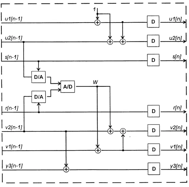
Figure 2-3 presents how each conversion block will be implemented in greater detail. The comparator output w[n] represents the sign of the difference between two
quantities according to the following relation between the digital inputs u2 and v2 and the
analog inputs s and r where s is the input signal and r is a reference signal:
w[n] = 1 if u2[n - 1]s[n - 1] > v2[n - 1 ]r[n - 1] (2-1) w[n]= 0 otherwise
The result w[n] is integrated to obtain the following results after the first, second, and
third order integrations:
ul[n] =n (2-2) n vl[n] = w[i] n(n + 3) u2[n] n(n + 3) (2-3) 2 v2[n] = w[] +w[i] y3[n] =y3[n- 1] +v2[n- 1] (2-4)
I
- -- ---u2[n]sn]
I--I
F
=Al
D/A -TJJ
I
" rIT
r
I
v2[ n"1m
-\.VFigure 2-3: Second order digital integration conversion block contents
r[n-1]
v2[n- 1] vlfn-11I
y3[n-1]
I
P. II I IThese values get passed down the pipeline and the resulting value for y3 at the end is an
accumulated average that represents the results of the A/D conversion according to the relation:
y3 [P]
s- (2-5)
u3[P]
where P is the total number of pipeline stages.
2.4 Pipelined Oversampling
In a conventional oversampling A/D converter, a certain number of samples
corresponding to the oversampling ratio is taken. After all the samples are taken, the decimator will output the result. Thus if the data is sampled every clock cycle, and converter has an oversampling ratio of 12:1, then for every 12 clock cycles a result is
obtained. With the use of pipelining, though, although latency would remain unchanged, throughput can be increased.
Pipelining is used in this converter design to eliminate some major limitations of conventional oversampling architectures. Using this technique, the modulator's feedback loop is distributed among a series of stages that process the input signal sequentially, as
shown in Figure 2-4. Each stage provides a digital signal to an also pipelined decimator. The decimator then accumulates the signals from the modulator in each stage and the final
output is the result at the end of the pipeline. Therefore oversampling is done in space rather than in time.
Mnrl II AT nD OVI'RSAMPLING IN TIME (R CYCLES / RESULT) H---- -. analoa MODULATOR signal -...0 Ith DECIMATOR
Figure 2-4: Comparison of oversampling techniques (a) Conventional (b) Pipelined
1) In conventional oversampling converters, output data rates are limited by the oversampling ratio. Both the modulator and the decimator need a number of clock cycles (equal to the oversampling ratio) to produce one digital result.
The converter is unable to read the next input value until it has calculated each output. On the other hand, in a pipelined system, the output data rate is only
DECIMATOR
Fil-\-I
-n
----dependent on the clock rate, since every clock cycle each stage can take another
input value, process it, and pass it down the pipeline. The result is that the
speed of the converter is no longer dependent on the resolution (oversampling
ratio). The speed is now determined by the clock rate while the resolution is
determined by the number of pipeline stages.
2) The inputs to pipelined and conventional architectures are also processed
differently. In a conventional system, the input to the modulator is allowed to
change while it is being processed. As a result, the signal cannot change rapidly
from the time the conversion starts to the time the result is ready or it will cause
signal distortion. In the pipelined system, the input is sampled at the first stage
and passed on to each subsequent stage. All the data accumulated to produce
each result comes from the same sampled input. Therefore the input signal is
allowed to have a higher bandwidth up to the Nyquist rate of the modulator
clock.
3) Another advantage of the pipelined system over the conventional system is the
fact that the pipelined architecture calculates each result independently from the
previous inputs. In conventional systems this is not the case, and therefore they
suffer from long output settling times in response to input step transitions.
One disadvantage of pipelining is the fact that many modulator stages are used to
This causes the result in the pipelined case to be susceptible to component mismatching.
3 Circuit Design
In this chapter, the final decimator implementation in terms of circuit design will
first be illustrated. Subsequently, the issues that were taken into consideration during the
circuit design stage and that led to the final design will be described. The goals desired to
achieve during this circuit design stage are 12-bit resolution at a 40MHz operation.
Power consumption should also be limited to 4mW per megasample per second. In addition, the area occupied by the circuit implementation should be an important
consideration.
3.1 Final Implementation Overview
The decimator is constructed from a series of twelve decimator blocks. Each
block in turn consists of five different stages, each of which performs a digital addition. The building block of each stage is a digital adder together with a delay latch. Following
is a description of each one of the building blocks that together constitute the decimator at
the following architecture levels: the adder, the parallel latch, the decimator block, and the
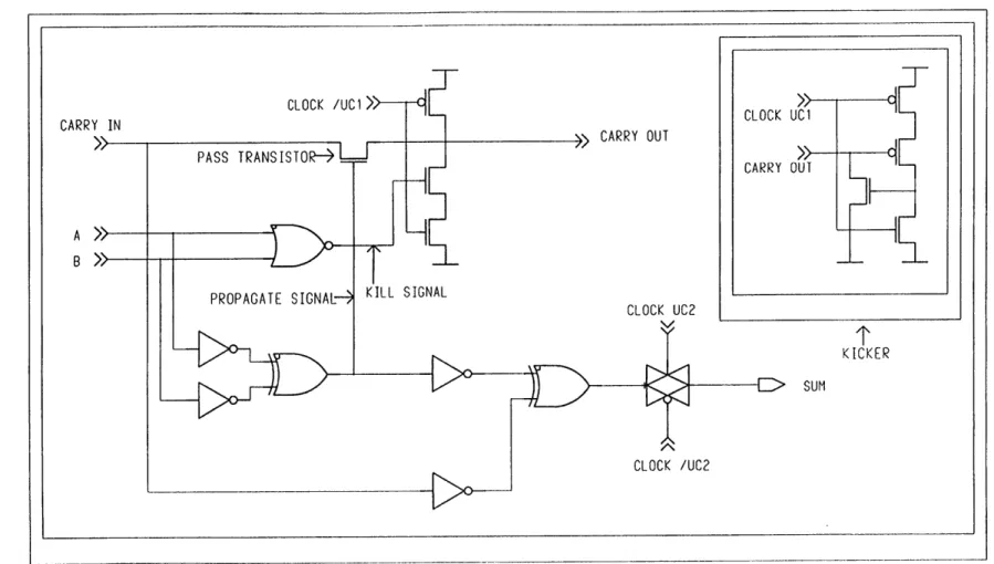
(a) Adder. The adder is the most important building block for each decimator block. It performs the actual computations that make the decimator function as a sinc3
filter.
The adder implementation used in this design and shown in Figure 3-1 is named a
Manchester Adder. In this type of an adder, the carry-bit chain consists of a series of pass
transistors, one for each bit-slice of the adder. Each node between the pass transistors
corresponds to the carry bit output of the corresponding bit-slice. This adder is designed
to operate in the "precharge-evaluate" mode. Under this mode of operation, a portion of
the clock cycle is used to precharge all the nodes in the carry-bit chain to a high value and
to read the new inputs into the circuit. This "precharge" step is followed by an "evaluate"
step during which the inputs are used to calculate the result as illustrated in Figure 3-2.
At the end of the "evaluate" step, the sum bits are latched by pass gates. Therefore, this
adder constitutes an addition function with a delay value of one entire clock cycle.
Each carry bit output is driven low by either the pass transistor or by a pull-down
structure. Otherwise, the node will remain floating with the high value it was precharged
with. Each of the driving mechanisms is individually controlled by two signals, a
"propagate" and a "kill" signal, produced by combinational logic during the "precharge" portion of the clock cycle using the two inputs to be added. When the "evaluate" cycle
starts, the carry bit values propagate down the pass transistor chain starting with the least
significant bit and by the end of the "evaluate" cycle, the last carry bit and the sum bits
have all settled to their final result. The carry bit chain is the critical path that determines
KICKER
SUM
Figure 3-1: Adder schematic
Unconditional Clock Timing Diagram
Figure 3-2: Unconditional clock timing diagram
It is worth noting that the case is possible in which a carry bit node that is to be
discharged does not necessarily have to be discharged by its own pull-down structure. In
such a case, the charge from a series of nodes must pass through several pass transistors
before getting discharged into ground. The more transistors this charge must pass
through, the slower the discharge process will be. This is why a structure called a "kicker"
was added to some of the nodes. This kicker becomes activated when it senses that the
node voltage is starting to drop and immediately provides a direct path to ground,
speeding up the discharge process.
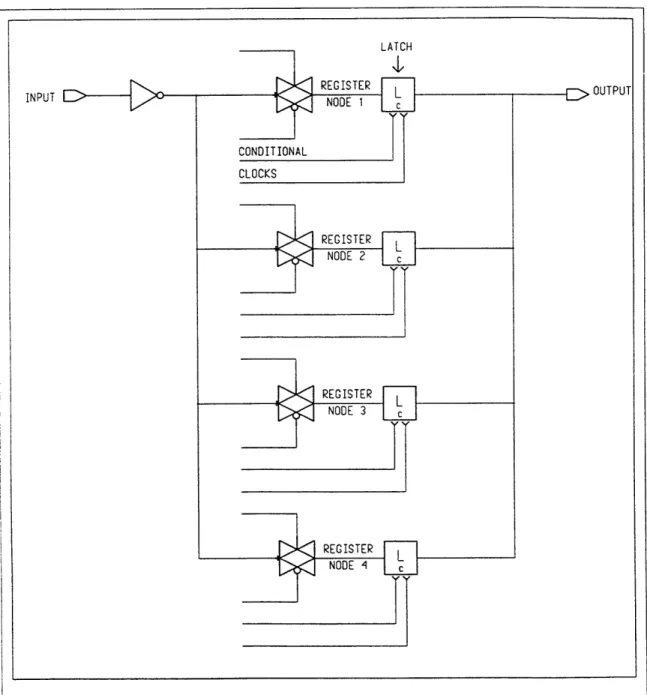
(b) Parallel Latch. The parallel latch is a modified implementation of a
three-latch delay and its schematic is shown in Figure 3-3. This parallel latch basically
0 2 Precharge Evaluate Latch Results T/4 Time T/2 3T/4 T Time
I ATCH
Figure 3-3: Parallel latch schematic
Figure 3-4: Conditional clock timing diagram
performs the equivalent of a series of three conventional latches but in a more
energy-efficient manner for reasons explained in detail later.
The parallel latch uses four conditional clocks and their inverses which follow the
sequence illustrated in Figure 3-4. Each clock ticks once every four cycles, one after the
other, that is, Conditional Clock 1 ticks at cycles 1, 5, 9, ...; Conditional Clock 2 ticks at cycles 2, 6, 10, ...; and so on. The parallel latch is designed to store a value every cycle in one of the nodes between the pass gate and the inverter latch and to release it three cycles
later, each node acting as a register. For example, after the 1st node stores a value, the
parallel latch cycles through the remaining three nodes, storing values in each of them.
Then after three clock cycles, as it stores a value in the 4th node, it releases the value in
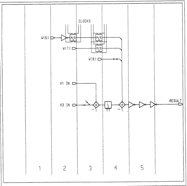
(c) Decimator Block. Each decimator block consists of five stages. Each stage represents each addition step, that is, each stage consists of one adder of the necessary
bit-width along with its parallel latch delay. Figure 3-5 shows the schematic for the basic
decimator block.
The schematic seems to be different from the functional diagram in Figure 2-3. Physically speaking, they are different but functionally they are not. The actual
implementation had to be modified to account for certain limitations that will be explained
later in greater detail.
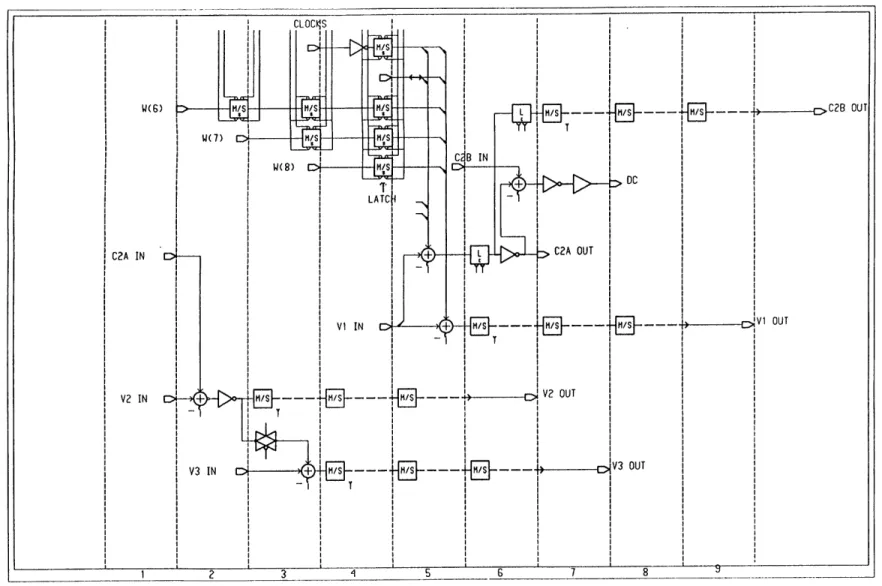
(d) Decimator. A series of twelve decimator blocks along with a final result generator compose the entire decimator section as shown in the schematic of Figure 3-6.
Also included in the schematic is the decimator control logic which produces the clocks
used by the adders and the conditional clocks used by the parallel latches.
The decimator receives data from the modulator and accumulates this data. Each
decimator block communicates with each modulator block to exchange information about
the signal being processed. The w signals carry the data from the modulator that will be
accumulated along each block. The dc signals carry feedback information back to the
modulator for comparison with the actual analog signal that is being converted. There
also are bus lines between the decimator blocks that carry the c2a and c2b signals as well
as the vl, v2, and v3 accumulation buses to the next block. The 12th block is followed by
a result generator, shown in Figure 3-7. The result from this generator is the actual
C2A IN
V2 IN
dec-btock-1
P
r-dec-bt ck-2
I
I
dec-bt ock-3I
I
_ Idec-bt ock-A~V
I
I
iN
dec-bI.ock-5I
I
I
I
I
dec-bl.ock-6 dec-btock-7I
I I
I
I
dec-btack-8I
I
I
I
I
dec-bt ockS9SI
I
I
I
dec-btock-10I
I
I
dec-block-11I
dc-btock-12I
I
r-es .generator C) Q 0 0 0>1"
11:
(1w
~zz
I I I I 1wr-
r-I cn I co r-CD C, C') w3.2 Design Issues
Following is an in depth discussion of the major issues that had in impact an the
design of the decimator circuitry and why certain implementations were chosen. These
issues are grouped into the four major hierarchy levels.
(a) Adder. As mentioned before, this decimator implementation consists of
various subsequent digital addition operations in order to perform the accumulation
function. This makes the adder implementation the section of the utmost importance of
the design as it contains the critical circuit path that will dictate how fast the entire
decimator can be clocked. Various adder implementations were considered. For example, the basic Ripple-Carry adder was the first one examined because of its simplicity. This
adder, though, was too slow for our needs. The time needed for the carry bit to ripple
through an entire chain of 12-bit adders was too long for the 40MHz clock. Another
adder considered was the Carry Look-Ahead adder. This adder is very fast, but the circuit
size grows exponentially with the number of bits required. Furthermore, the speed of such
an adder was faster than required.
The Manchester adder seemed to be the most attractive option. It performed up to
our speed requirements and, at the same time, it provided a linear relationship between
bit-width and circuit size. The implementation did not require much more hardware per
bit than the ripple-carry adder but, in turn, provided a considerable boost in terms of
by making relatively simple changes such as transistor sizes and the use of kickers. This
allows for relatively quick and easy changes in the future in case a faster performance is
desired. Power consumption was also acceptable for our needs.
As mentioned earlier, the carry bit chain is the critical path of the circuit where the
worst case situation occurs when a low value must be propagated through the entire chain. Care was taken to make sure that, in this worst case, the propagation process could
properly finish under a 40MHz operation. One way to accomplish this was through the
use the kickers described earlier. The goal is to use the kickers to speed up the worst case
propagation but to use the least number of kickers possible in order to reduce power
consumption. Through simulation, it was determined that for bit-widths larger than 7, a
kicker is necessary at the 4th bit position. If the bit-width is 12 then an additional at the
7th bit position is necessary.
In addition to the use of kickers, transistor sizes are very important in maximizing
the speed of the carry chain. The pass transistor was enlarged in order to support more
current flow and transistors in the pull-down and kicker structures were made as small as
possible in order to minimize the diffusion capacitance that they add to the nodes. Figure
3-8 shows the propagation of a zero-carry value through the entire carry bit chain of a 12-bit adder. The rise of the clock shown indicates the end of the "evaluate" stage, the
time by which the carry bit should have settled.
The circuitry used for the XOR gates, as shown in Figure 3-9, is very sluggish
because current must pass through two transistors to drive the output and the internal
0 5e-09 le-08 1.5e-08 2e-08 2.5e-08 3.le-08 3.5e-08 4e-08
X (Time:sec) Base
Figure 3-8: Carry bit chain propagation plot
at a high speed. In this adder though, the output of one XOR gate needs to be the input to another XOR gate, which is itself a decently heavy load for the driving XOR. In addition, the result from the driving XOR must have settled by the end of the "precharge" stage because the propagate signal must be ready for proper results in the carry bit propagation. For this reason, an inverter was used as a buffer in between. In addition, inverting buffers are used in each one of the inputs to the XOR gates to isolate the XOR inputs from the
3.5 '' ='Clock1z .5Bi 0 "it U 1.091 -0.5 3.5 O.027 ' -0.5 3.5 2 ~095 -0.51 3.53 -0.5 3.54 -0.5 3*5 ~~~5 .0-00EF 23. ... >- -0.51 --a) 3.5 ed 0.5 r-r-4 3.5 00. 0.51 3.5 8 0.01461 -0.51 1 I I I I I I 3.5 9 -0.5 3.5 10 -0.5 35 F 0.0203'9
Figure 3-9: XOR gate schematic
preceding circuitry and ensure that those inputs will have a proper drive strength. Figure
3-10 shows how the evaluation of the propagate signal is properly completed by the end of the "precharge" stage, as indicated by the fall of the clock shown.
It is worthy to mention that the two clocks used to control the "precharge-evaluate" process and the latching must be nonoverlapping. Nonoverlapping clocks prevent the racing conditions that might occur if the "precharge" stage were to start before the output pass gate is closed or if the output pass gate were to open before a following latch closes.
(b) Parallel Latch. The parallel latch was the result of the need to reduce power consumption throughout the decimator after preliminary simulations indicated that the power consumption was too high. The previous implementation consisted of using three
('l.nck
Figure 3-10: "Propagate" signal plot
conventional latches to delay the output of the adders in one block by three clock cycles
before being released into the next block. The problem with this implementation is that
for every cycle there are 4 clock transitions with 3 transistor gates connected to each clock, amounting to 12 transistor transitions per cycle. The more transistor gate transitions per cycle, the greater the gate load on the clock drivers, that is, the greater the capacitance which needs to be discharged upon a clock transition.
The design of the parallel latch contains 8 clocks with 2 transistors connected to each clock line. This amounts to 16 transistor transitions per 4 cycles, or 4 transistor gate
3.5 3 2.5 2 1.5 1 0.5 0 J 4 0 3.5 3 2.5 2 1.5 1 0.5 0 -0.5
transitions per cycle. This is a considerable gain over the conventional latch delay in terms
of power consumption.
(c) Decimator Block. One main limitation in the design of the decimator block is
the fact that the modulator takes too long to produce the w(8:4) signals that get
accumulated at each stage. Therefore, instead of delaying the signals until all the w bits
are ready, the operations are started with just the most significant bits w(4:5) (For the w
signals the most significant bit is index 4. Instead of indicating the bit position, the index
is indicative of the time delay at which each bit is available.). The operations for bits
w(6:8) are then delayed until the next block. The process that in the functional diagram is performed in one block is instead spread out over two blocks in the actual implementation.
This has a negative impact on the accuracy of the dc signal but this impact is negligible.
It must be noted that due to the fact that one functional block is spread over two
implemented blocks, there are signal buses, such as v2 and v3, that are not created until
Block 2 and, therefore, operations with those signals are unnecessary. In order to save
chip area and power, these unnecessary operations were eliminated from those blocks.
Likewise, Block 12 needs not to provide any more dc signals since no more w signals need
to be calculated by the modulator, making some operations there also unnecessary. The
result is an implementation for Blocks 1, 2, and 12 that are different from the basic block.
Figure 3-12: Decimator Block #2 schematic
C2B OUT
VI OUT
(d) Decimator. The result generator is the section of the decimator which adds the last set ofw bits to the accumulation buses in order to produce the final result. This is
necessary because as mentioned earlier, the w signal addition is performed over the time space of two blocks. So after Block 12 has produced a result, still bits w(6:8) corresponding to modulator Block 12 need to be added to the accumulation buses. The
result generator is not considered to be a block because it does not provide the modulator
with any feedback signals for the processing of the final answer. Its only function is to add
4 Layout Design
In this chapter, the final decimator implementation from the layout design
perspective will first be illustrated. Afterwards, the issues that were taken into
consideration during the layout design stage and that led to the final design will be
described. The main goal to achieve in the layout design stage was in terms of
dimensions. Lengthwise, the decimator could not exceed a length of 6.2mm. (The chip is
6.9mm in length and width but about 0.7mm are reserved for input/output pads and output
drivers.) In terms of area, the decimator must allow enough space on the chip for the
modulator section. Also taken into consideration throughout the layout design was power
consumption.
4.1 Final Implementation Overview
In terms of layout, the decimator is organized following the same hierarchy levels
described in Chapter 3. This design overview, contains a description of the final layout
implementations for the adder and parallel latch and how they are arranged to form the
decimator blocks and, ultimately, the decimator.
(a) Adder. The layout for an individual adder is shown in Figure 4-1. All the components of the adder are arranged in a vertical stack, alongside of which run the
71 .un
OUTPUT PASS GATE
LEL LATCH INVERTER
LATCHES CONDITIONAL CLOCKS
Figure 4-2: Parallel Latch layout
power lines vdd and vss, the input nodes a and b, the output node, and the carry-bit chain.
The input/output signal flow within the adder is from left to right, and the carry bit line
flows upward, as indicated by the cin and cout signals.
Space was left in the area underneath the adders to allow placement of
components, such as pass gates, latches, and inverters, that are not considered part of the
adder but that are necessary for the proper function of each decimator block. This space
is also used for the placement of kickers wherever they are necessary.
(b) Parallel Latch. The layout of the parallel latch is shown in Figure 4-2. It can be observed from the layout that the parallel latch is organized into two stacks of components. The leftmost stack contains the four input pass gates that belong to each register while the rightmost stack contains the four output latches that belong to each register. The input inverter that buffers the input to the four pass gates is not located with the latch itself for reasons that will later be explained. There are three bundles of four clock lines each running through the parallel latch, two on the two outer edges which
CONOITIONAL CLOCKS C3NOITIONAL CLOCKS
carry the same clocks, and one between the two component stacks. The signal flow in the
parallel latch is also towards the right as can be observed from the input and output node
locations.
(c) Decimator Block. Figure 4-3 shows a bit-slice of a decimator block. It shows five adders in a row followed by a stack of four parallel latches. There are four parallel
latches since only four of the adders need to be latched. The inputs flow from the leftmost
extreme of the block to the corresponding adders, the outputs of which then flow through
the block to their corresponding parallel latches. The outputs from the parallel latches
finally run to the rightmost extreme of the block where they are passed on to the next
block.
The layout for a basic decimator block, particularly Block 3, is shown in Figure
4-4. This figure illustrates how a block is composed of a stack of bit-slices. At the
bottom and at the top it can be observed that there are some empty spaces where adders
would be expected. This is due to the fact that additions are not necessary at those bit
positions. Visible at the top and at the bottom of the block, are many power lines and
clock lines. The lines on the lower left hand corner are the w signals that come from the
modulator blocks and on the lower right hand corner are the dc signals that run to the
modulator blocks.
(d) Decimator. Figure 4-5 shows the layout of the entire decimator. It consists of a row of twelve blocks followed by the result generator. At the top left-hand corner is
STAGES
INPUT!
POWER LINES
OUTPUTS
L
W SIGNALS CLOCK SIGNALS DC SIGNALS
AND POWER LINES
LOWER BUS
G.inn
Figure 4-5: Decimator layout
E E r-p o\ OUTPUT BUS
located the decimator control logic. Along the top and bottom boundaries of the
decimator, two bus lines can be noticed. The upper bus carries power feeds and the lower
bus carries power feeds and clock feeds that distribute the clocks throughout the entire
decimator. Also protruding from the bottom of the decimator, are the w and dc lines that
nm to and from the modulator. On the rightmost extreme of the decimator is the output
bus which collects all the bits from the result generator and runs to the chip's output pads.
4.2 Design Issues
Following is a discussion of the major issues that had in impact in the design of the
decimator layout as well as how, in some instances, layout design led to changes in the
circuit implementation. These issues are again grouped into the four major hierarchy
levels mentioned earlier.
(a) Adder. The most significant issue in creating the layout for the adder was whether to arrange all the components within it in one vertical stack, as it is now, or divide
them into two stacks side by side. At the time, there were too many unknowns. The
exact number of conversion blocks that would be included in the design was unclear.
There was also uncertainty concerning the space the modulator blocks would require. In
addition, it was uncertain which chip size would be able to fit our design. All these factors
would directly affect which layout scheme would be the best to use for the adders.
Since the answers to these questions were unknown, the amount of space available
would occupy more horizontal space. If the decimator was too long, it would not fit
along one side of the chip and would have to be split into two sections. Splitting the
decimator into two sections would have required substantial amounts of area for the wire
buses that would carry the signals from the output of one section to the input of the other.
Preventing that from happening became a main goal. By using the one-stack scheme, there was a good chance of preventing this since it would occupy less horizontal space. It
would occupy more vertical space and more area, though, and most important of all, it
would make the metal lines of the carry-bit chain longer as well as clock lines, increasing
the capacitive load on those nodes. This meant using larger transistors to drive the
carry-bit chain nodes and higher power consumption for each clock transition.
By making an area study with both layout configurations, it became clear that the
larger chip must be used regardless of the configuration used. At that time, the number of
blocks that were to be included in the design was also determined. It was then decided to
use the one-stack configuration. With this scheme, the decimator would fit without the
need to divide it into two sections. It should be pointed out that if the decimator had been
divided into two sections, the increase in area used would have caused problems fitting the
whole design even on the larger chip that had been chosen. The increased vertical space
was not as critical and the increased area became less of an issue as substantially more
space was available in the larger chip. The longer carry-bit metal lines and clock lines
were acceptable as long as the division of the decimator into two sections could be
The layout cell for the adder was compressed as much as possible in order to
minimize vertical and horizontal dimensions. This was actually one of the most time
consuming and dedicated tasks. In doing so, a substantial number of process design rules
were pushed to the limit. It was necessary to fully customize and optimize the layout for
this application as opposed to using already existing generic component cells because the
existing ones, designed for easy placement, are not area optimized and their use would
have resulted in a decimator too large to be practical. The disadvantage of fully
customizing and optimizing the adder components is that, since everything is very tightly
packed, changes require extensive work.
(b) Parallel Latch. In creating the layout for the parallel latch, one of the most important issues was the type of latch to use on the output. The two options, shown in
Figure 4-6, were the pass gate latch and the clocked inverter. In terms of functionality, the pass gate latch performs better with a slightly faster rise time. On the other hand, the
clocked inverter is better in terms of layout since it is significantly more space efficient.
Figure 4-7 compares both layout constructions for the four stacked latches needed by the parallel latch. The clocked inverter is considerably better, mostly because it requires only
two rows of diffusion contacts as opposed to three. This achieves an ample savings in
area over the pass gate latch.
The parallel latch, as mentioned before, consists of two stacks, one with the input
pass gates and one with the output latches. It was convenient to group them in such a
(a)
(b)
I.--i
L
(b)
Figure 4-7: Latch layout (a) Clocked inverter (b) Pass gate latch
structuring the parallel latch in this way, also makes it possible to vertically stack the four
parallel latches needed for each block bit-slice, with the height of the stack being almost
exactly equal to that of the adder. It is also designed so that the bundle of clock lines
passing through the center can be shared between both stacks, saving power during clock
transitions.
It was mentioned earlier that the buffering inverter for the input pass gates was not
located within the parallel latch. This was mainly due to that fact that there was not
enough space to include this inverter. It was more convenient to place that inverter in the
space left open within the adder layout. This also is of an advantage since some of the
outputs from the adders need to travel long distances before reaching the latches and the
inverters serve as buffers.
- - - - - -
-(D
On On
(c) Decimator Block. The decimator block was also designed to minimize the capacitive load on the clocks. This was done by sharing clock lines between the adders as
much as possible. Due to the fact that the clocks used by the adders are different than
those used by the parallel latches, the adders and the latches were grouped into separate
sections of the block so that they could share their own clock lines.
(d) Decimator. When looking at the decimator in Figure 4-5, it can be noticed that each block looks different. Since the decimator performs a series of accumulation
operations in each block, the bit-width of the vl, v2, and v3 buses within each block
gradually increases as they move down the pipeline. It is therefore possible to trim the adders and include only the bits that span the width of the bus at each individual block. In
this way, each block was customized to save power. This was done carefully not to make
the bus too small since overflows would ruin the final result.
Since the bit-width of the adders in the first five blocks is relatively short, the decimator control logic was placed in that area, allowing for a more efficient use of chip area. The clock drivers from the control logic are then connected to the lower bus by means of wires that run through the blocks. Only one bus is necessary to run the clocks to each block and the lower bus was chosen to do this. The reason for using only one bus to carry clock lines is because having the upper bus carry clock lines as well would have unnecessarily raised the load on the clock drivers with the extra metal. In addition, by connecting into the blocks from the bottom and eliminating the clock lines from the upper bus, this allowed the clock lines to be trimmed in the upper sections of each block so that
they would not extend any further than the adders they needed to reach. To even further
reduce capacitance, the widths of many clock lines was reduced where possible. By
means of these techniques, the capacitance in many of the clock line nodes was greatly
reduced, in some cases by even half.
The upper bus, only carrying power lines, also serves a purpose. With the clock
lines, it would be detrimental, as explained above, to include them in the upper bus. But
since power lines never undergo transitions, it is actually beneficial because capacitance in
the power lines helps smooth out the noise and fluctuations that are so characteristic of
5 Results
The research and design efforts described resulted in an effective implementation
of the decimator that satisfied all the requirements. The most important requirement, speed, was achieved for clocking rates of 40MHz and at a resolution of 12 bits. The chip
area was minimized by achieving dimensions of 6.1mm in length and 1.7mm in height.
The length did not exceed the 6.2mm length specification and permitted proper routing of
the output bus. In terms of area, it allowed for comfortable fitting of the modulator in the
remaining space. For illustration, the layout for the entire A/D converter chip is shown in
Figure 4-8.
The power consumption was minimized to 1.9mW per megasample per second, below the 4mW per megasample per second specification. Tables 4-1 and 4-2 illustrate
how capacitance and power consumption are distributed among the internal nodes and
clock lines for both the decimator and modulator sections of the design. Due to the fact
that the decimator operates with a 3.3V supply, power consumption by this section is
overshadowed by that of the modulator sections operating with a 5V supply.
Nevertheless, due to the large amounts of metal used in the decimator, the potential exists
for significant power consumption. Through reduction of capacitance, this potential was
reduced to produce the results shown in the figure.
The result was also, very importantly, a design that can easily be modified to
DECIMATOR
SMODULATOR
Figure 5-1: AID Converter chip layout
to operate at speeds at least 25% higher under the current design's 1.2 micron process by just adding kickers along the carry-bit chain. In addition, the design can be easily modified
to support higher oversampling ratios. With the design's modular arrangement of blocks
and adders, the procedure is simplified to a few steps of changing adder array sizes in a
Capacitance Breakdown
by Chip Section
Section pF Decimator Internal 461 Decimator Clocks 401 Modulator Internal 567 Modulator Clocks 844Table 4-1: Capacitance Breakdown by Section
Power Breakdown by Chip Section
Section mW/MSPS* Percent Decimator Internal (3V) 1.04 8% Decimator Clocks (3V) 0.9 7% Modulator Internal (3V) 0.77 6% Modulator Clocks (3V) 0.76 6% Modulator Internal (5V) 3.01 23% Modulator Clocks (5V) 6.71 51% Total 13.19 100%
*MSPS=Mega Samples Per Second
6 Concluding Remarks
There are various ways of implementing digital adders, most of them
compromising area or power for speed. The appropriate implementation that satisfies the
speed requirement but at the same time minimizes the power and area for this application
was determined. Determining the appropriate adder was a critical task since the overall
design uses a considerable number of adders and can amount to considerable power
consumption and area needs.
Once the primary issue of the speed requirement was met, the power consumption
was reduced to satisfy the required overall converter specifications. Techniques were
used to optimize the power consumption such as eliminating unnecessary components, minimizing the transistor sizes appropriately according to the output driving loads, and
eliminating unnecessary metal lines.
Steps were also taken to minimize chip area. A number of pipeline conversion
blocks were arranged in such a way that space efficiency was maximized and layout
simplicity maintained. This provided two main advantages. First, certain techniques, such
as sharing metal lines between stages, reduced area as well as cut power consumption by
reducing the capacitive loads on components. Second, efforts to minimize the area aided
in using the smallest chip size possible and therefore considerably reducing fabrication costs.
The implementation of the pipelined decimator for the oversampling A/D converter here described, is therefore a promising development for future pipelined converters that
will be developed under this continuing program. The ease with which operating speed can be increased and pipelined blocks can be added to increase the oversampling ratio are the most attractive features of this design because they accommodate for future needs. Also improvements in device fabrication processes will lead to more possible improvements in terms of speed, power consumption, and area.
The chip containing the decimator design is currently in the process of fabrication and is to be tested upon receipt.
Bibliography
[1] J.C. Candy, G.C. Temes, "Oversampling Methods for A/D and D/A Conversion," Oversampling Delta-Sigma Data Converters, IEEE Press, pp. 1-25, 1991.
[2] J.C. Candy, "Decimation for Sigma Delta Modulation," Delta-Sigma Data Converters, IEEE Press, pp. 400-404, 1991.
Oversampling
[3] S.R. Norsworthy, R. Schreier, G.C. Temes, "Decimation and Interpolation for Sigma Delta Conversion," Delta-Sigma Data Converters, IEEE Press, pp. 406, 1997.