HAL Id: hal-01916367
https://hal.archives-ouvertes.fr/hal-01916367
Submitted on 20 Nov 2018
HAL is a multi-disciplinary open access
archive for the deposit and dissemination of
sci-entific research documents, whether they are
pub-lished or not. The documents may come from
teaching and research institutions in France or
abroad, or from public or private research centers.
L’archive ouverte pluridisciplinaire HAL, est
destinée au dépôt et à la diffusion de documents
scientifiques de niveau recherche, publiés ou non,
émanant des établissements d’enseignement et de
recherche français ou étrangers, des laboratoires
publics ou privés.
Electrografted monolayer based on a naphthalene
diimide–ruthenium terpyridine complex dyad: efficient
creation of large-area molecular junctions with high
current densities
Denis Frath, van Quyen Nguyen, Frédéric Lafolet, Pascal G.P. Martin,
Jean-Christophe Lacroix
To cite this version:
Denis Frath, van Quyen Nguyen, Frédéric Lafolet, Pascal G.P. Martin, Jean-Christophe Lacroix.
Elec-trografted monolayer based on a naphthalene diimide–ruthenium terpyridine complex dyad: efficient
creation of large-area molecular junctions with high current densities. Chemical Communications,
Royal Society of Chemistry, 2017, 53 (80), pp.10997 - 11000. �10.1039/C7CC04972B�. �hal-01916367�
COMMUNICATION
DOI: 10.1039/c7cc04972b
Electrografted Monolayer Based on a Naphthalene
Diimide-Ruthenium Terpyridine Complex Dyad: Efficient Creation of
Large-area Molecular Junctions with High Current Densities
Denis Frath, Van Quyen Nguyen, Frédéric Lafolet, Pascal Martin, Jean-Christophe Lacroix*
An electron donor-acceptor dyad has been designed for the creation of large-area molecular junctions (MJ). Diazonium cation electrografting was used to form well controlled monolayers. The robustness of the monolayer enabled the creation of MJs using direct top-coat evaporation with a high yield of operating devices.
Given the number of potential applications in molecular electronics, including switches, memories, transistors and rectifiers, the development of new molecular systems with multifunctional properties is of great importance.1 Donor-bridge-acceptor chemical structures have been proposed as the stereotypical building units for molecular rectifiers.2 Since then many electron-donor-acceptor dyads have been incorporated in Molecular Junctions (MJ).3–7 Some of them use metal complexes because of their rich redox and photophysical properties.8–10 Azulene-bridged coordinated framework11 and platinum-based metallo-supramolecular polymers12 were recently reported to act as rectifiers even though the rectification ratio (RR) remains modest. High RR were obtained using liquid mercury as the top electrode in a porphyrin/fullerene bilayer device13 or using self-assembled alkylferrocene monolayers, contacted by chemisorption to a bottom electrode and physisorption to a top electrode.14,15 These devices are among the best molecular rectifiers to date but their fabrication techniques suffer from the intrinsic stability limit of the SAM-based layer and the eGaIn contact. More recently, ferrocene, has been combined with a polychloro-triphenylmethyl unit to control the RR by changing the electronic nature of the component.16
Different strategies have been used to construct the active layer, including Langmuir-Blodgett techniques,17,18 layer-by-layer assembly11,12 and electrochemical deposition. Diazonium electroreduction19 is one of the best techniques, as the electrogenerated layers are compact, strongly adherent to the metal surface and pinhole-free. Consequently it is possible to evaporate the top electrode directly onto the molecular layer, which makes the creation of devices based on this approach very attractive.20,21 Electrografting from organometallic diazonium derivatives has been reported22–24 and was used to
develop memories25 or MJ with robust bipolar light emission and charge transport properties.26
Naphthalene diimide (NDI) derivatives are commonly used electron acceptors in many organic electronic devices..27 Recently they have been used to create various type of MJ that show moderate rectification properties.28,29 Combining both Ru complexes and NDI results in donor-acceptor systems with multiple redox states.28 Such systems could be of interest for memories or rectifiers. In order to investigate these aspects we have developed a new graftable dyad for the creation of large-area molecular junctions.
The molecular structure was designed with an NDI electron-accepting unit based on covalently bound to a ruthenium bisterpyridine complex (Scheme 1). The bridging phenyl ring is expected to decouple the two subunits. Steric hindrance between the hydrogen of this phenyl ring and the NDI oxygen atoms induces a large twist with respect to the NDI plane that should limit delocalization.31 A hexyl chain was introduced to enhance solubility. The structure also features a phenylamine terminal group in order to enable in-situ preparation of a diazonium cation and subsequent grafting onto various substrates. The first synthetic step consists of the preparation of the alkylated precursor 1 by condensation of 1,4,5,8-naphthalene-tetracarboxylic dianhydride and hexylamine. A previously reported procedure was adapted to introduce (4-aminophenyl)-2,2’:6’,2”-terpyridine (tpyPhNH2) and to
generate NDI 2.30 The resulting ligand was then complexed with the (4-aminophenyl)-2,2’:6’,2”-terpyridine ruthenium trichloride (Ru[tpyPhNH2]Cl3) precursor using procedures
already reported.32 Silica gel chromatography followed by counter-ion exchange was used to afford pure dyad 3 (NMR and HRMS are provided in Supporting Information files). The electrochemical behavior of a solution of 3 (0.5 mM in MeCN + 0.1M TBAPF6) was studied by cyclic voltammetry (CV)
Scheme 1. Synthetic pathway towards dyad 3: (i) C6H13NH2, DMF, reflux, 40% (ii)
tpyPhNH2, isoquinoline cat., m-cresol, 200°C, 74% (iii) Ru[tpyPhNH2]Cl3, Et3N,
EtOH, Reflux, 18%
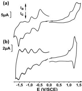
The curve displays two waves in the positive potential range, corresponding to the irreversible aniline oxidation at Epa= 1.08
V/SCE and the quasi-reversible oxidation of the Ru metal center at E1/2 = 1.32 V/SCE. In the negative region, there are
four partially reversible one-electron waves at E1/2 = -0.52
V/SCE and E1/2 = -0.95 V/SCE, corresponding to the reduction
of the NDI fragment, and at E1/2 = -1.30 V/SCE and E1/2 = -1.49
V/SCE, corresponding to the reduction of the terpyridine ligands. Compared to the reference compound Ru(tpy)2PhNH2,
there was no significant effect of the electron-withdrawing NDI fragment on oxidation of the ruthenium complex. Moreover, the complex only slightly affects the reduction waves of NDI (Table S1 and Figure S1 and S2). These results suggest that conjugation through the central phenyl group connecting the donor and acceptor parts of dyad 3 is negligible.
The diazonium cation derived from dyad 3 was generated in-situ by addition of 15 eq. of tert-butyl nitrite (experimental details in Supporting Information). Ten successive cycles of the electrochemical reduction between 0 and -0.5 V/SCE were run on the resulting solution (Figure S3). In the first reduction cycle the irreversible peak at ca. -0.25 V/SCE corresponds to diazonium reduction. In the following cycles, the current intensity decreases, which suggests that dyad 3 is being grafted onto the surface. The electrochemical behavior of the modified electrode was studied by CV (Figure 1b and Table S1). Reversible oxidation of the ruthenium occurs at E1/2 = 1.32
V/SCE. The region of negative potential displays four reversible waves corresponding to the reduction of the NDI fragment at E1/2 = -0.50 V/SCE and E1/2 = -0.93 V/SCE, and for the reduction
of the terpyridine ligands at E1/2 = -1.24 V/SCE and E1/2 =
-1.53V/SCE. The additional peaks at Epa= 1.01 V/SCE and Epc=
-0.72 V/SCE could be explained by a charge trapping phenomenon.33 Similar behavior of electrografted layers of Ru-complexes has been reported.22 After a few scans in oxidation or in reduction, these peaks decrease and the film remains stable upon further cycling (Figure S4). Integration of the peaks gives an apparent concentration of ca. 4.8x10⁻¹⁰ mol.cm-2. Taking bulkiness into account, it is consistent with values below 20x10-10 mol.cm-2 usually observed for close-packed monolayers of aromatic core such as nitrobenzene.34
Figure 1. Cyclic voltammetry of dyad 3 (a) in MeCN (0.5 mM), TBAPF6 0.1M on GC
at 0.1 V/s. (b) grafted layer on GC in MeCN, TBAPF6 0.1M at 0.1 V/s
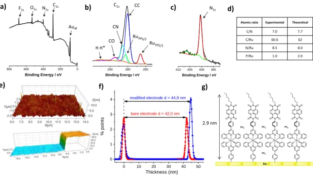
To further characterize the dyad 3 layer obtained by electro-grafting, a gold electrode was modified by running ten successive cycles between 0 and -0.5 V/SCE. X-Ray photo-electron spectroscopy (XPS) was used to characterize the film (Figure 2a and Table S2). The attenuation of the Au4f signal of the modified substrate compared to a bare gold electrode indicated that the film is 2.7 nm-thick. This value is consistent with the molecular length obtained by molecular modeling (2.9 nm) and excludes the formation of multilayer. A characteristic peak at 281.4 eV can be assigned to Ru(II) 3d5/2. The
corresponding Ru(II) 3d3/2 peak at 285.4 eV is masked by the
C1s signal (Figure 2b). On top of the main C1s peak at 285.1 eV, several other signals can be attributed to terpyridine ligand CN bonds at 286.3 eV, NDI imide CO bonds at 288.7 eV and a π-π* satellite due to aromatic cores at 292.4 eV. The single narrow N1s peak at 400.1 eV in the high-resolution spectra rules out the possibility of azo-bridged grafting (Figure 2c).23 Experimental atomic ratios for C, N and Ru reproduce fairly well the expected composition of the layer (Figure 2d). The P/Ru ratio is approximately half the theoretical value. This can be rationalized by the fact that the first reduction of the grafted NDI occurs at E1/2 = -0.5V/SCE. Since this potential is
reached during grafting, the radical-anion of the NDI is formed and compensates one of the two charges on the ruthenium complex. It is reasonable to think that a PF6 counter-ion is
consequently removed from the film.
Gold microelectrodes (ca. 20 μm x 2 cm and 50 nm-thick on Si/SiO2) were functionalized with dyad 3 using the same
electrografting conditions described above. The presence of the molecular layer was confirmed by AFM (Figure 2e). Surface topography reveals a roughness of ca. 0.8 nm, of the same order of magnitude as that observed for bare electrodes (ca. 0.6 nm). This shows that the molecular layer is quite densely packed and homogeneous. The thickness of the molecular layer is measured using the cross-sections of the modified and unmodified gold steps.
-1,5 -1,0 -0,5 0,0 0,5 1,0 1,5 E (V/SCE) 2µA Ia 5µA Ic
(a)
(b)
Figure 2. Characterization of Dyad 3 functionalized gold electrodes: (a) XPS survey (b) C1s-Ru3d high-resolution XPS spectra (c) N1s high-resolution XPS spectra (d) atomic ratio of
the layer determined by XPS (e) AFM topography of the surface 5x5 μm2 (top) and cross section (bottom) of the modified nanostructured electrode corresponding to the thickness
measurement, (f) AFM statistical analysis of the thickness, fitted with gaussian (g) schematic representation of the monolayer.
A histogram of the height data is fitted by two separate Gaussian functions, with the height expressed as the difference between the centers of the two functions and the uncertainty given by the quadrature addition of the two best-fit σ values (Figure 2f). It gives an average value of 2.9 nm, close to the length of the molecule and confirming that the film is a monolayer (Figure 2g).
Next, the modified microelectrodes were used to create MJs using photo-lithography step (see SI files). The top contact electrode was obtained by direct evaporation of Ti (2 nm) and Au (30 nm) onto the 2.9 nm-thick organometallic layer. Large-area molecular junctions were fabricated; current density vs. applied voltage (J-V) curves are presented in Figure 3. A high yield in operating junctions is reached (80%, 24 out of 30 junctions fabricated) showing that the monolayer is robust enough to enable MJ creation despite the fact that the top electrode is directly evaporated. This yield can be compared with that found when SAM-based monolayers are used: only 1.2% of the devices "work".35 Another interesting feature is that very high current densities were reached: 9 A/cm2 was observed when a bias of -2.5 V was applied. This has to be compared with current densities below 1mA/cm2 in MJ incorporating alkane chains bearing redox moities, which are limited by the large attenuation factor of the chains.15,16 Moreover, J-V curves feature an asymmetric profile with a higher current density when the bottom electrode is negatively polarized at a moderate potential of -2.5 V. In other words, the preferred electron flow is from the donor to the acceptor moities, i.e. anti-Aviram rectification. Similar behavior was observed with several systems3,4 while opposite preferred current flows havebeen reported for bilayer MJ.29 The average rectification ratio observed at -2.5V for the 24 operating junctions is 300 (see SI file for an histogram) and can
be compared to recent results ranging from 350 to 2800 at 2.5V6 or close to 900 in few junctions36 with EGaIn top contact. Note also that a value 105 was recently obtained but associated with low current density due to alkane moities.37
Figure 3. a) schematic illustration of the junction. b) JV and semilogarithmic JV
curve for Au/dyad 3 monolayer/Ti/Au MJ with standard and log-standard deviations (7 junctions have been tested).
The exact mechanism behind the direction of the observed rectification is beyond the scope of this study and will be the subject of a more detailed article. Let us just recall that rectification behavior can be reversed when the effective tunneling distance between the electrode is changed by using redox moities incorporated at various distances from the electrodes,38 or when the relative strength of the coupling between the molecular layer and the top or bottom electrode is changed.39 Further investigation is needed to understand the rectifying properties of the present MJ, and we anticipate that they may be tuned and controled by changing the initial redox state of the molecular junction and the amount of counter-ion incorporated in the device.
Atomic ratio Experimental Theoretical
C/N 7.0 7.7 C/Ru 60.6 62 N/Ru 8.5 8.0 P/Ru 1.0 2.0 280 285 290 Binding Energy / eV Ru3d5/2 Ru3d3/2 CC CN CO π-π* 395 400 405 410 Binding Energy / eV 0 10 20 30 40 50 0 1 2 3 4 modified electrode d = 44,9 nm % po in ts Thickness (nm) bare electrode d = 42,0 nm
c)
d)
e)
a)
b)
N1s 0 200 400 600 800 Binding Energy / eV C1sg)
N1s C1s Au4f O1s F1sf)
2.9 nm -2 -1 0 1 2 -9 -6 -3 0 Curr en t Den si ty (A.c m -2) Applied potential (V)a)
b)
-3 -2 -1 0 1 2 3 -15 -10 -5 0 5 Ln (J ) Applied Potential / VTo conclude, a donor-acceptor dyad has been designed for the creation of large-area molecular junctions. This system can be conveniently grafted by diazonium electroreduction to form well controlled monolayers on various substrates. Films on glassy carbon characterized by cyclic voltammetry showed five stable redox states. Modified gold electrodes were obtained and fully characterized by XPS and AFM. The robustness of dyad 3 monolayer on gold substrates makes it possible to create large-area molecular junctions in high yield despite direct metal deposition on the monolayer. Thanks to the very low thickness of the device and the molecular structure of dyad 3, the current densities through these MJ are several orders of magnitude higher than those observed for other monolayer-based devices. Moreover, strong rectification behavior was observed with prefered electron transport from the donor to the acceptor moities. Detailed mechanisms of this asymmetric charge transport are being investigated in order to better understand this phenomenon and to optimize the rectification ratio of these very promising monolayer-based electronic devices.
We thank the the Centre National de la Recherche Scientifique, and Agence Nationale de la Recherche (ANR-15-CE09 0001-01) for their financial support. We also warmly thank B. Lemarque and P. Decorse for XPS analyses and discussions.
Notes and references
1 D. Xiang, X. Wang, C. Jia, T. Lee and X. Guo, Chem. Rev., 2016,
116, 4318–4440.
2 A. Aviram and M. A. Ratner, Chem. Phys. Lett., 1974, 29, 277– 283.
3 R. M. Metzger, Chem. Phys., 2006, 326, 176–187. 4 R. M. Metzger, Chem. Rev., 2015, 115, 5056–5115.
5 G. Jayamurugan, V. Gowri, D. Hernández, S. Martin, A. González-Orive, C. Dengiz, O. Dumele, F. Pérez-Murano, J.-P. Gisselbrecht, C. Boudon, W. B. Schweizer, B. Breiten, A. D. Finke, G. Jeschke, B. Bernet, L. Ruhlmann, P. Cea and F. Diederich, Chem. Eur. J., 2016, 22, 10539–10547.
6 M. S. Johnson, R. Kota, D. L. Mattern and R. M. Metzger,
Langmuir, 2016, 32, 6851–6859.
7 J. E. Meany, M. S. Johnson, S. A. Woski and R. M. Metzger,
ChemPlusChem, 2016, 81, 1152–1155.
8 H. J. Bolink, L. Cappelli, E. Coronado, M. Grätzel and M. K. Nazeeruddin, J. Am. Chem. Soc., 2006, 128, 46–47. 9 A. Hagfeldt, G. Boschloo, L. Sun, L. Kloo and H. Pettersson,
Chem. Rev., 2010, 110, 6595–6663.
10 T. Nagashima, H. Ozawa, T. Suzuki, T. Nakabayashi, K. Kanaizuka and M. Haga, Chem. Eur. J., 2016, 22, 1658–1667.
11 S. Sun, X. Zhuang, L. Wang, B. Zhang, J. Ding, F. Zhang and Y. Chen, J. Mater. Chem. C, 2017, 5, 2223–2229.
12 C. Chakraborty, R. K. Pandey, M. D. Hossain, Z. Futera, S. Moriyama and M. Higuchi, ACS Appl. Mater. Interfaces, 2015, 7, 19034–19042.
13 S. P. Koiry, P. Jha, D. K. Aswal, S. K. Nayak, C. Majumdar, S. Chattopadhyay, S. K. Gupta and J. V. Yakhmi, Chem. Phys. Lett., 2010, 485, 137–141.
14 C. A. Nijhuis, W. F. Reus and G. M. Whitesides, J. Am. Chem.
Soc., 2009, 131, 17814–17827.
15 L. Yuan, R. Breuer, L. Jiang, M. Schmittel and C. A. Nijhuis, Nano
Lett., 2015, 15, 5506–5512.
16 M. Souto, L. Yuan, D. C. Morales, L. Jiang, I. Ratera, C. A. Nijhuis and J. Veciana, J. Am. Chem. Soc., 2017, 139, 4262–4265. 17 L. D. Wickramasinghe, S. Mazumder, S. Gonawala, M. M. Perera,
H. Baydoun, B. Thapa, L. Li, L. Xie, G. Mao, Z. Zhou, H. B. Schlegel and C. N. Verani, Angew. Chem., Int. Ed., 2014, 53, 14462– 14467.
18 M. S. Johnson, L. Wickramasinghe, C. Verani and R. M. Metzger,
J. Phys. Chem. C, 2016, 120, 10578–10583.
19 J. Pinson and F. Podvorica, Chem. Soc. Rev., 2005, 34, 429–439. 20 P. Martin, M. L. Della Rocca, A. Anthore, P. Lafarge and J.-C.
Lacroix, J. Am. Chem. Soc., 2012, 134, 154–157.
21 A. P. Bonifas and R. L. McCreery, Nature Nanotech., 2010, 5, 612–617.
22 B. Jousselme, G. Bidan, M. Billon, C. Goyer, Y. Kervella, S. Guillerez, E. A. Hamad, C. Goze-Bac, J.-Y. Mevellec and S. Lefrant, J. Electroanal. Chem., 2008, 621, 277–285. 23 C. Agnes, J.-C. Arnault, F. Omnes, B. Jousselme, M. Billon, G.
Bidan and P. Mailley, Phys. Chem. Chem. Phys., 2009, 11, 11647–11654.
24 V. Q. Nguyen, X. Sun, F. Lafolet, J.-F. Audibert, F. Miomandre, G. Lemercier, F. Loiseau and J.-C. Lacroix, J. Am. Chem. Soc., 2016,
138, 9381–9384.
25 T. Cabaret, L. Fillaud, B. Jousselme, J. O. Klein and V. Derycke, in
14th IEEE International Conference on Nanotechnology, 2014,
pp. 499–504.
26 U. M. Tefashe, Q. V. Nguyen, F. Lafolet, J.-C. Lacroix and R. L. McCreery, J. Am. Chem. Soc., 2017, 139, 7436–7439. 27 X. Guo, A. Facchetti and T. J. Marks, Chem. Rev., 2014, 114,
8943–9021.
28 X. Lefèvre, F. Moggia, O. Segut, Y.-P. Lin, Y. Ksari, G. Delafosse, K. Smaali, D. Guérin, V. Derycke, D. Vuillaume, S. Lenfant, L. Patrone and B. Jousselme, J. Phys. Chem. C, 2015, 119, 5703– 5713.
29 A. Bayat, J.-C. Lacroix and R. L. McCreery, J. Am. Chem. Soc., 2016, 138, 12287–12296.
30 O. Johansson, M. Borgström, R. Lomoth, M. Palmblad, J. Bergquist, L. Hammarström, L. Sun and B. Åkermark, Inorg.
Chem., 2003, 42, 2908–2918.
31 M. Kondratenko, A. G. Moiseev and D. F. Perepichka, J. Mater.
Chem., 2011, 21, 1470–1478.
32 M. Jacquet, F. Lafolet, S. Cobo, F. Loiseau, A. Bakkar, M. Boggio-Pasqua, E. Saint-Aman and G. Royal, Inorg. Chem., 2017, 56, 4357–4368.
33 Charges are stored in the film during grafting or reduction and oxidation scans. The peaks at 1.01 V/SCE and -0.72 may be assigned to the detrapping of these charges.
34 P. A. Brooksby and A. J. Downard, Langmuir, 2004, 20, 5038– 5045.
35 T.-W. Kim, G. Wang and T. Lee, Nanotechnology, 2007, 18, 315204/1–315204/8.
36 Qiu, Y. Zhang, T. L. Krijger, X. Qiu, P. van’t Hof, J. C. Hummelen and R. C. Chiechi, Chem. Sci., 2017, 8, 2365–2372.
37 X. Chen, M. Roemer, L. Yuan, W. Du, D. Thompson, E. del Barco and C. A. Nijhuis, Nature Nanotech., 2017, 12(8):797-803 38 L. Yuan, N. Nerngchamnong, L. Cao, H. Hamoudi, E. del Barco,
M. Roemer, R. K. Sriramula, D. Thompson and C. A. Nijhuis, Nat.
Commun., 2015, 6, 6324.
39 S. Sherif, G. Rubio-Bollinger, E. Pinilla-Cienfuegos, E. Coronado, J. C. Cuevas and N. Agraït, Nanotechnology, 2015, 26, 291001.