HAL Id: hal-00118633
https://hal.archives-ouvertes.fr/hal-00118633
Submitted on 26 Feb 2007
HAL is a multi-disciplinary open access archive for the deposit and dissemination of sci-entific research documents, whether they are pub-lished or not. The documents may come from teaching and research institutions in France or abroad, or from public or private research centers.
L’archive ouverte pluridisciplinaire HAL, est destinée au dépôt et à la diffusion de documents scientifiques de niveau recherche, publiés ou non, émanant des établissements d’enseignement et de recherche français ou étrangers, des laboratoires publics ou privés.
Ultra-fast relaxation of electrons in wide-gap dielectrics
Hans-Joachim Fitting, Vsevolod S. Kortov, Guillaume Petite
To cite this version:
Hans-Joachim Fitting, Vsevolod S. Kortov, Guillaume Petite. Ultra-fast relaxation of electrons in wide-gap dielectrics. Journal of Luminescence, Elsevier, 2007, 122-123, pp.542-545. �hal-00118633�
Ultra-fast relaxation of electrons in wide-gap dielectrics
H.-J. Fittinga, , , V.S. Kortovb and G. PetitecaPhysics Department, University of Rostock, Universitätsplatz 3, D-18051 Rostock, Germany bUrals State Technical University, Mira street 19, RUS-620002 Ekaterinburg, Russia
cLaboratoire des Solides Irradies, Ecole Polytechnique, UMR CEA-DSM/CNRS, F-91128
Palaiseau Cedex, France
Abstract
Low-energy electrons scattered in the conduction band of a dielectric solid should behave like Bloch electrons and will interact with perturbations of the atomic lattice, i.e. with phonons. Thus the phonon-based description of low-energy scattering within an energy band structure of a solid bears certain advantages against common free-electron scattering mechanisms. Moreover, the inelastic scattering is described by the dielectric energy loss function. With these collective scattering models we have performed the simulation of excited electron relaxation and attenuation in the insulator SiO2. After excitation to a mean initial energy of
several eV their energy relaxation occurs within a short time interval of 200 fs to full thermalization. There is a very rapid impact ionization cooling connected with cascading of electrons at the beginning during the first 10 fs, followed by much slower attenuation due to phonon losses in wide-gap dielectrics and insulators.
Keywords: Electron impact ionization; Cascading; Electron–phonon interaction; Electron attenuation; Thermalization
PACS classification codes: 77.33.Gm; 34.80; 79.20.Hx
1. Introduction
Over more than three decades silicon dioxide stands for the most important dielectric and insulating material in microelectronics and optics. The favourable electronic and optical features of SiO2 are based on the wide forbidden gap of 9 eV in the electronic energy band
structure and the natural compatibility in the highly developed silicon technology.
Perfect thin dielectric and optical SiO2 layers, often with a well-defined interface to the silicon
substrate, are mostly investigated by optical and electron spectroscopy, i.e. photoluminescence and cathodoluminescence. The latter one allows a probing within smallest volumina in sub-micron dimension. For this reason the electron scattering and transport should be thoroughly understood. Therefore, the electronic excitation processes with rapid carrier excitation and relaxation should be investigated. The related fast conduction electron dynamics in optical breakdown processes under high-intensity laser excitation has been investigated in Ref. [1], and the photo- and exoelectron emission after radiation excitation and relaxation in Refs. [2] and [3]. The high-energy charge injection and the subsequent relaxation occur in ultra-short time scales and should be considered in the following.
2. Monte Carlo Simulation of impact ionization and
phonon scattering
The full Monte Carlo (MC) program of low-energy electron scattering, especially in dielectric materials and insulators is mainly based on impact ionization and electron–phonon interaction and has been described in Refs. [4], [5] and [6].
2.1. Longitudinal optical (LO) phonons
The scattering frequency of electrons with energy E in a parabolic band with LO phonons of energy ωLO and Bose population NLO is given according to the Fröhlich theory, see, e.g.
Ref. [7]: 2 * 2 0 1 1 1 1 1 1 ln 4 2 2 2 1 1 LO LO LO LO LO E e m f N E E ω ω πε ε∞ ε ω ⎡ + ± ⎤ ⎛ ⎞ ⎛ ⎞ = ⎜⎝ + ⎟⎠×⎜ − ⎟ ⎢ + ± ⎥ ⎢ ⎥ ⎝ ⎠ ⎣ ⎦ m h m h h m h (1)
where the upper signs stand for phonon absorption (−) and the lower ones for phonon emission (+) m* is the effective electron mass, ε and ε∞ are the dielectric permittivities on the
left- and right-hand side from the ionic polarization, i.e. the static and the optical dielectric constant, respectively. In SiO2, we use ε 3.84 and ε =2.25∞ distributed to two LO modes
ωLO=150 and 60 meV.
2.2. Acoustic (a.c.) phonons
After the optical runaway and heating-up to energies in the eV region the electrons feel a stronger acoustic (a.c.) coupling with the lattice. The energy loss or gain with some meV is much less than the energy of hot electrons. Therefore this a.c. scattering is considered as nearly elastic.
A strong increase of a.c. scattering is obtained at higher electron energies of some eV. In order to avoid irreal high a.c. scattering rates at high energies Bradford and Woolf [8] have introduced a Coulomb-like screening, leading to the following expressions:
(
)
( )
2 2 . . . . 4 2 1 / ln 1 1 / D qBZ a c a c BZ m N A E E f E D E E E A E π ρ ω + A A ⎡ ⎤ ⎛ ⎞ ⎛ ⎞ = ⎜ ⎟ ×⎢ ⎜ + ⎟− ⎥ + ⎝ ⎠ ⎣ ⎝ ⎠ ⎦ hh (2)with D(E) as the density of states (DOS) and the effective electron mass mD, Ea.c. is the
acoustic deformation potential, A one screening parameter, ρ the mass density, EBZ the
electron energy at the Brillouin zone (BZ) boundary kBZ, NqBZ and ωBZ are acoustic phonon
2.3. Impact ionization (i.i.)
At still higher electron energies E>Eg exceeding the forbidden gap Eg between valence and
conduction band, direct valence band ionization, called impact ionization (i.i.), becomes possible.
Stobbe et al. [9] have calculated the transition rate between parabolic bands and found an appropriate formula: . . 2 2 1 ln 1 a th i i th th th E E E f C DE E E ⎡ − ⎛ ⎞⎤ = ⎢ + ⎜ ⎟⎥ ⎝ ⎠ ⎣ ⎦ for E E> (3)
This is an expression including the soft ionization threshold of Keldysh proportional to
(E-E )th 2, as well as a hard threshold behaviour of the Bethe type: ln(E/E )th .
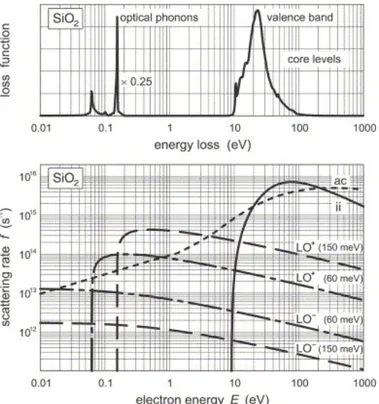
In Fig. 1, the dielectric loss function Im(-1/ε(ω)) due to excitation of LO phonons and to ionization of valence band electrons (i.i.) are presented in the upper part, further on the respective scattering rates of all mechanisms. Eqs. (1)–(3) are given in the lower part of Fig. 1. The detailed material scattering parameters can be found in Ref. [5].
Fig. 1. Dielectric energy loss function (above) and corresponding scattering rates of electrons with longitudinal optical (LO) phonons of energies ω1=150 meV and ω2=60 meV; LO+ phonon emission, LO− phonon
annihilation; then with acoustic (a.c.) phonons, and due to impact ionization (i.i.) of valence band electrons in SiO2 corresponding to the dielectric energy loss function above.
3. Fast electron relaxation in the conduction band
The development of new “pump and probe” techniques by means of ultra-short laser pulses allows to resolve the time-dependent relaxation of inner photoelectrons (PE) in photoluminescence (PL) and photoelectron emission spectroscopy [1] or electron beam-induced secondary electrons (SE) in cathodoluminescence (CL) spectroscopy [10]. According to the electron energy loss function in SiO2 (Fig. 1) the excited inner SE possess initial
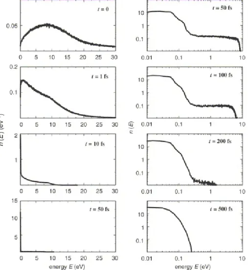
energies of some tens of eV [4] and [5]. In the first step after creation the energy of SE is decaying rapidly due to very fast impact ionization and cascading under 10 eV after 10 fs. This process is demonstrated in Fig. 2 and Fig. 3.
Fig. 2. Energy ralaxation of excited secondary electrons with time t. The rapid cooling at the beginning - t<10 fs - is due to impact ionization and cascading, the slower attenuation over 200 fs mainly due to the emission of LO phonons.
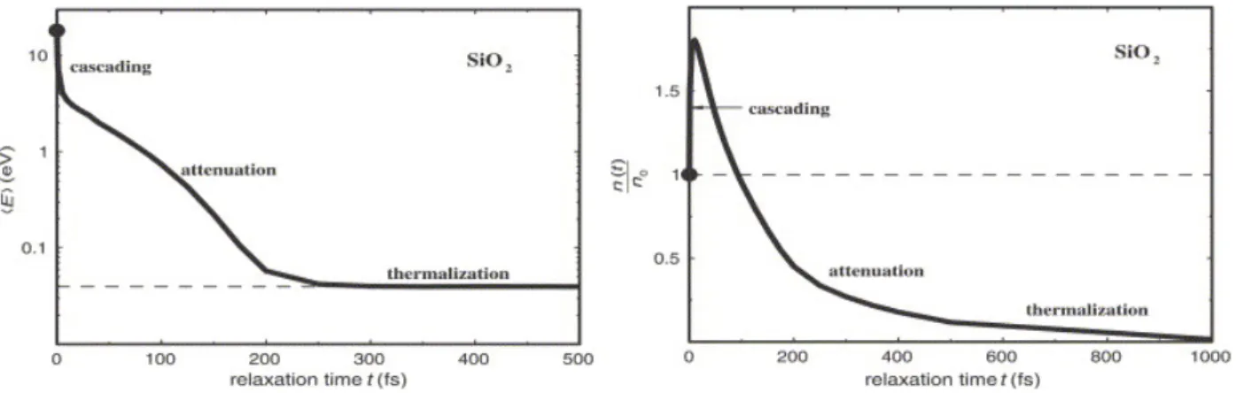
Afterwards the electrons are exposed to phonon interaction and are cooled down much slower till they are almost thermalized after about 200 fs. Their mean energy E in Fig. 3 (top) shows rapid cooling at the beginning due to impact ionization and cascading, then a much slower attenuation down to the thermalization at E ≈40 meV corresponding to the lattice temperature T≈300 K according to the Boltzmann statistics: E =3/2 kT. This fairly
instantaneous agreement is really surprizing. In the lower part of Fig. 3, the number n(t) of electrons related to their initial concentration n0 is plotted versus time t and we clearly observe
the three steps; cascading, attenuation, and thermalization again. Spontaneous thermalization below the lattice temperature, i.e. 40 meV, should lead to electron–hole recombination and the electron vanishes from the conduction band. So after about several ps we find the electrons as almost recombined or trapped. These processes occur over very short time scales in SiO2
because of the high impact ionization rates with a great energy loss of ΔE>9 eV and the subsequent energy losses due to a relatively high LO phonon mode ωLO=150 meV as described in Fig. 1 and demonstrated in Fig. 3.
Fig. 3. Mean secondary electron (SE) energy <E> (left) and the SE rate n/n0 (right) during the relaxation time t,
with rapid cooling due to impact ionization and cascading at the beginning followed by slow attenuation due to phonon emission, final thermalization, and recombination.
Acknowledgements
We are grateful to the support by the INTAS project 01-0458 “Fast electronic processes in dielectrics”.
References
[1] G. Petite, 4th International Conference on Electric Charges in Non-conductive Materials, Tours, France, July 2001, Proceedings Vide CSC’4, p. 516.
[2] V.S. Kortov, V. Isakov, A. Gaprindoshvily, H.J. Fitting, H. Glaefeke and W. Wild, Phys.
Status Solid A 54 (1979), p. 633.
[3] A. Zatsepin, V.S. Kortov and H.J. Fitting, J. Non-cryst. Solids 351 (2005), p. 869.
[4] H.J. Fitting, E. Schreiber, J.C. Kuhr and A. von Czarnowski, J. Electron Spectros. Relat.
Phenom. 119 (2001), p. 35.
[5] E. Schreiber and H.J. Fitting, J. Electron Spectros. Relat. Phenom. 124 (2002), p. 25. [6] E. Schreiber and H.J. Fitting, J. Electron Spectros. Relat. Phenom. 131–132 (2003), p. 87. [7] J. Llacer and E.L. Garwin, J. Appl. Phys. 40 (1969), p. 2766.
[8] J.N. Bradford and S. Woolf, J. Appl. Phys. 70 (1991), p. 490.
[9] M. Stobbe, A. Könis, R. Redmer, J. Henk and W. Schattke, Phys. Rev. B 44 (1991), p. 11105.
[10] H.J. Fitting, T. Barfels, A.N. Trukhin, B. Schmidt, A. Gulans and A. von Czarnowski, J.