HAL Id: hal-02514784
https://hal.archives-ouvertes.fr/hal-02514784
Submitted on 22 Mar 2020
HAL is a multi-disciplinary open access
archive for the deposit and dissemination of
sci-entific research documents, whether they are
pub-lished or not. The documents may come from
teaching and research institutions in France or
abroad, or from public or private research centers.
L’archive ouverte pluridisciplinaire HAL, est
destinée au dépôt et à la diffusion de documents
scientifiques de niveau recherche, publiés ou non,
émanant des établissements d’enseignement et de
recherche français ou étrangers, des laboratoires
publics ou privés.
High voltage SiC MOSFET Opportunities for Dielectric
Barrier Dis- charge Transformerless Power Supply
Mame Andallah Diop, Antoine Belinger, Hubert Piquet
To cite this version:
Mame Andallah Diop, Antoine Belinger, Hubert Piquet. High voltage SiC MOSFET Opportunities for
Dielectric Barrier Dis- charge Transformerless Power Supply. 6th Euro-Asian Pulsed Power Conference
(EAPPC 2016), Sep 2016, Estoril, Portugal. �hal-02514784�
High voltage SiC MOSFET Opportunities for Dielectric Barrier
Dis-charge Transformerless Power Supply
M.A. Diop, A. Belinger, H. Piquet*
LAPLACE, Université de Toulouse, CNRS, INPT, UPS, France 118 Route de Narbonne, 31000 Toulouse, France.
*hubert.piquet@laplace.univ-tlse.fr From an electrical point of view, cold plasmas are
com-plex loads to control. For ignition, high voltages are re-quired, and once established, the plasma can easily go into the arc regime (thermal plasma). In Dielectric Barrier Discharge (DBD) setups, at least one dielectric is placed between the two metallic electrodes that supply the gas. Current flowing through the plasma also charges these dielectrics: their voltages increase and the gas voltage also decreases. Through this limiting mechanism, the dielectric barriers limit the current and therefore prevent from going into the arc regime. This property makes the DBD partic-ularly appealing in various applications that require plas-mas with low temperatures: UV excimer lamps, thin film deposition, surface treatment, disinfection. Our develop-ments are geared toward DBD UV lamps [1], but the ap-proach proposed is applicable to any DBD setup (plane-plane setup for thin film deposit was also tested). The capacitive character of the dielectrics requires sup-plying DBDs using an alternative source. Furthermore, to ignite the discharge at atmospheric pressure, the required voltage usually reaches several kilovolts. This high alter-nating voltage is traditionally obtained via amplification using a step-up transformer. Unfortunately, the parasitic capacitances of the latter (inter-turn and inter-winding) limit the power transfer: these capacitances have general-ly low values but often are of the same order of magni-tude as those of the DBD. It is parallel to the DBD, so it diverts a significant proportion of the current transferred. This slows down the voltage rise and delays the ignition. This increases the OFF time, during which the excited species created by the previous discharge disappear. In some processes this can even change the behavior of the discharge. As a matter of fact, the main consequences of the parasitic capacitance of the transformer concern the functioning of the discharge and not the energetic effi-ciency of the system.
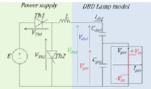
These reasons incited us to investigate power supplies for DBD without transformer. To our knowledge, only theo-retical developments have been proposed to date [2], high-voltage switches being available only for a few years. Our solution is to directly connect a high-voltage current-pulsed [3] quasi-resonant inverter to the DBD, as presented on Figure 1. It involves using high-voltage switches: the required characteristics are thyristor-like behavior (closing switches with spontaneous turn-off at null current), but actual thyristors have frequency limita-tions which make them incompatible for DBD applica-tions. Several solutions for such synthetized devices are evaluated, tested experimentally, and compared, including
10kV-10A SiC power DMOSFETs designed by CREE (single switch and series connection).
Figure 1: Power supply and DBD electrical model
The design and implementation of a converter’s prototype are presented and tested with a DBD UV lamp [1]; we especially detail the implementation of high voltage MOSFETs, and the control board designed in order to sustain the high voltage insulation.
Experiments highlight the topology’s performances and the effects of the 10kV SiC switch characteristics on the discharge and on the efficiency: the main advantage of the converter is its transformerless operation, with a reduced number of switches. We demonstrate the feasibility of using 10kV SIC MOSFETs in transformerless supply for DBD. For our knowledge, it is the first time that these switches are used in a pulsed current converter for DBD. However using 10kV SiC MOSFET presents a serious drawback in this topology: the OFF state MOSFETs voltage reach up several kV (E); when turn ON takes place, the parasitic capacitance is shortened and its stored energy (Coss.E2/2) dissipated. These losses are inherent to
our application and depend on the E operating voltage but not on the power transferred to the DBD. For increased efficiency of the converter, these 10kV SiC MOSFET should be preferently selected for high power DBDs.
References
[1] M. I. Lomaev, V. S. Skakun, E. A. Sosnin, V. F. Tarasenko, D. V. Shitts, M. V. Erofeev, “Excilamps
efficient sources of spontaneous UV and VUV radiation”
Phys.-Uspekhi, vol. 46, no. 2, pp. 193–209, Feb. 2003. [2] A. El-Deib, F. Dawson, G. Zissis “Transformer-less
current controlled driver for a dielectric barrier discharge lamp using HV silicon carbide (SiC) switching devices” IEEE Energy Conversion Congress and
Exposition, pp.1124-1131, 17-22 Sept. 2011
[3] R. Diez, H. Piquet, D. Florez, X. Bonnin, "Current-Mode Approach in Power Supplies for DBD
Excilamps: Review of 4 Topologies", IEEE Transactions